-
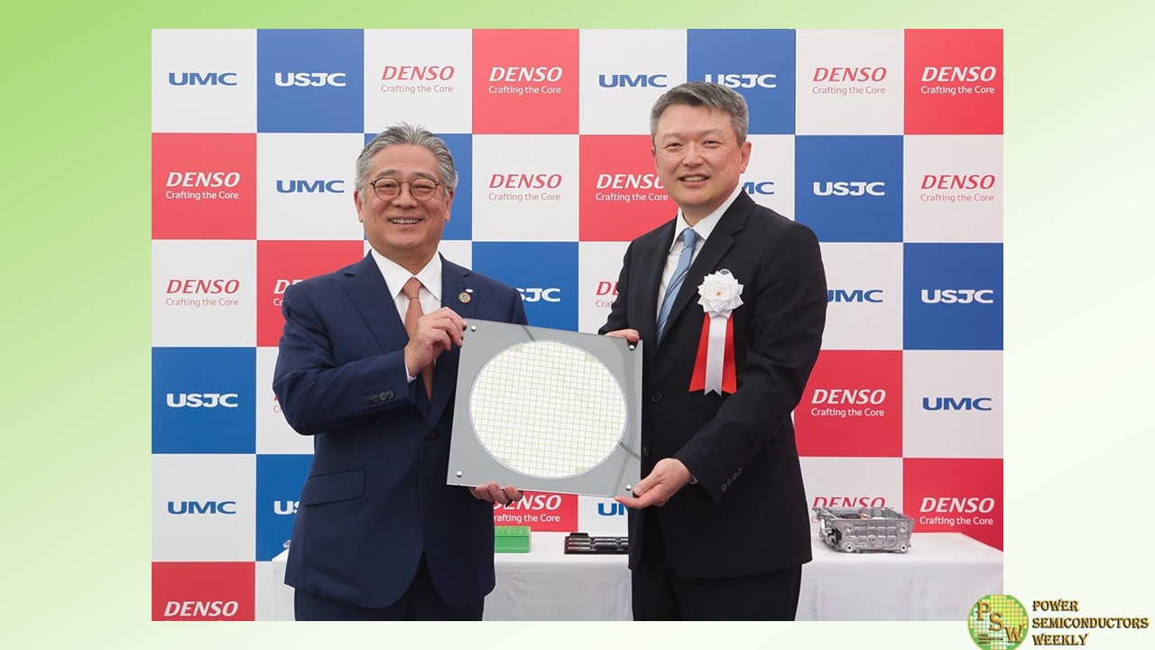
DENSO CORPORATION (DENSO), a leading mobility supplier, and United Semiconductor Japan Co., Ltd. (“USJC”), a subsidiary of global semiconductor foundry United Microelectronics Corporation (“UMC”), announced a joint collaboration to produce insulated gate bipolar transistors (IGBT), which have entered mass production at the 300mm fab of USJC. A first shipment ceremony was held last week to mark this important milestone. It comes just one year after the companies announced a strategic partnership for this critical power semiconductor used in electric vehicles.
As adoption of electric vehicles accelerates, automakers are seeking to boost powertrain efficiency while also increasing cost-effectiveness of electrified vehicles. The jointly invested line at USJC supports the production of a new generation of IGBT developed by DENSO, which offers 20% reduction in power losses compared with earlier generation devices. Production is expected to reach 10,000 wafers per month by 2025.
The ceremony was held at USJC’s fab in Mie Prefecture, Japan. Attendees included by DENSO President Koji Arima, UMC Co-President Jason Wang, USJC President Michiari Kawano, Director-General of the Commerce and Information Policy Bureau at Japan’s Ministry of Economy, Trade and Industry (METI) Satoshi Nohara, Governor of Mie Prefecture Katsuyuki Ichimi, and Mayor of Kuwana City Narutaka Ito.
“Today, we are thrilled to welcome a memorable shipping ceremony that symbolizes the partnership between DENSO, UMC and USJC. We are from different cultures such as semiconductor industry and automobile industry. However, we have worked steadily with mutual respect which is a source of our strong competitiveness. DENSO, together with our trusted partners, will continue to further accelerate electrification through the production of competitive semiconductors in order to preserve the global environment and create a society full of smiles,” said Koji Arima, President of DENSO.
“USJC is proud to be the first semiconductor foundry in Japan to manufacture IGBT on 300mm wafers, offering customers greater production efficiency than the standard fabrication on 200mm wafers. Thanks to our dedicated teams and support from DENSO, we were able to complete trial production and reliability testing without delay and honor the mass production date as agreed with the customer,” said Michiari Kawano, President of USJC.
“It is an honor to be a strategic partner of DENSO, a leading automotive solution provider to global automakers. This collaboration fully demonstrates UMC’s manufacturing capability and our collaborative approach to ensure the success of our foundry customers,” said Jason Wang, Co-President of UMC. “The electrification and automation of cars will continue to drive up semiconductor content, particularly for chips manufactured using specialty foundry processes on 28nm and above nodes. As a specialty technology leader, UMC is well positioned to play a bigger role in the automotive value chain and enabling our partners to capture opportunities and win market share in this rapidly evolving industry.
Original – DENSO
-

Power Integrations, the leader in gate-driver technology for medium- and high-voltage inverter applications, introduced the SCALE-iFlex™ LT NTC family of IGBT/SiC module gate drivers. The new gate drivers target the popular new dual, 100 mm x 140 mm style of IGBT modules, such as the Mitsubishi LV100 and the Infineon XHP 2, as well as silicon carbide (SiC) variants thereof up to 2300 V blocking voltage. The SCALE-iFlex LT NTC drivers provide Negative Temperature Coefficient (NTC) data – an isolated temperature measurement of the power module – which enables accurate thermal management of converter systems. This is particularly important for systems with multiple modules arrayed in parallel, ensuring proper current sharing and dramatically enhancing overall system reliability.
Thorsten Schmidt, product marketing manager at Power Integrations, commented: “Designers of renewable energy and rail systems using SCALE-iFlex drivers already benefit from increased system performance; the SCALE-iFlex approach handles paralleling so expertly that one module in five can be eliminated without loss of performance or current de-rating. Adding an isolated NTC output reduces hardware complexity – particularly cables and connectors – and contributes to system observability and overall performance.”
Based on Power Integrations’ proven SCALE™-2 technology, SCALE-iFlex LT gate drivers improve current sharing accuracy and therefore increase the current carrying capability of multiple-paralleled modules by 20 percent, allowing users to significantly increase the semiconductor utilization of their converter stacks. This is possible because the localized control of each 2SMLT0220D MAG (Module Adapted Gate driver) unit ensures precise control and switching, enabling excellent current sharing. Advanced Active Clamping (AAC) is employed to deliver accurate overvoltage protection.
To further increase space saving, up to four MAG-driven power modules can be parallel-connected from a single 2SILT1200T Isolated Master Control (IMC) unit, which can also be mounted on a power module due to its compact outline. The gate drivers are fully qualified to IEC 61000-4-x (EMI), IEC-60068-2-x (environmental) and IEC-60068-2-x (mechanical) specifications, and undergo complete type testing – low voltage, high voltage, thermal cycling – shortening designer development time by 12 to 18 months. A comprehensive set of protection features is included, and parts are optionally available with conformal coating.
Original – Power Integrations
-
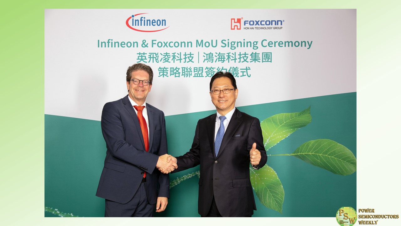
Infineon Technologies AG, the global leader in automotive semiconductors, and Hon Hai Technology Group (“Foxconn”), the world’s largest electronics manufacturing services provider, aim to establish a long-term partnership in the field of electric vehicles (EV) to jointly develop advanced electromobility with efficient and intelligent features. The Memorandum of Understanding (MoU) focuses on silicon carbide (SiC) development, leveraging Infineon’s automotive SiC innovations and Foxconn’s know-how in automotive systems.
“The automotive industry is evolving. With the rapid growth of the EV market and the associated need for more range and performance, the development of electromobility must continue to advance and innovate,” said Peter Schiefer, President of the Infineon Automotive Division. “Infineon’s commitment and passion for innovation and zero-defect quality has made us the best partner for our customers. We look forward to writing a new chapter in electromobility together with Foxconn.”
“We are pleased to be working with Infineon and are confident that this collaboration will result in optimized architecture, product performance, cost competitiveness and high system integration to provide customers with the most competitive automotive solutions,” said Jun Seki, Foxconn’s Chief Strategy Officer for EVs.
According to the MoU, the two companies will collaborate on the implementation of SiC technology in automotive high-power applications like traction inverters, onboard chargers, and DC-DC converters. Both parties intend to jointly develop EV solutions with outstanding performance and efficiency based on Infineon’s automotive system understanding, technical support and SiC product offerings combined with Foxconn’s electronics design and manufacturing expertise and the capability of system-level integration.
In addition, the two companies plan to establish a system application center in Taiwan to further expand the scope of their cooperation. This center will focus on optimizing vehicle applications, including smart cabin applications, advanced driver assistance systems and autonomous driving applications. It will also address electromobility applications such as battery management systems and traction inverters. The collaboration covers a wide range of Infineon’s automotive products, including sensors, microcontrollers, power semiconductors, high-performance memories for specific applications, human machine interface and security solutions. The system application center is expected to be established within 2023.
Original – Infineon Technologies
-
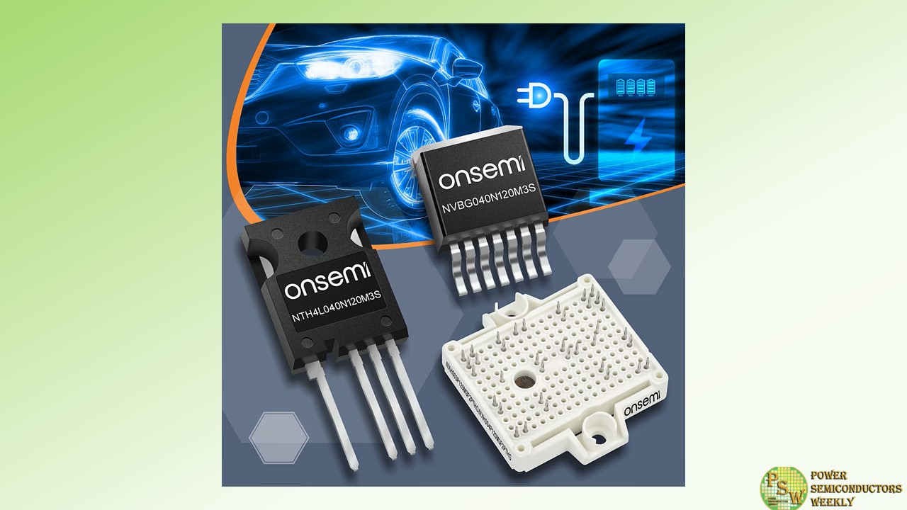
onsemi, a leader in intelligent power and sensing technologies, announced the release of the latest generation of 1200 V EliteSiC silicon carbide (SiC) M3S devices, which enable power electronics designers to achieve best-in-class efficiency and lower system cost. The new portfolio includes EliteSiC MOSFETs and modules that facilitate higher switching speeds to support the growing number of 800 V electric vehicle (EV) on-board charger (OBC) and energy infrastructure applications, such as EV charging, solar and energy storage systems.
Also, part of the portfolio, are new EliteSiC M3S devices in half-bridge power integrated modules (PIMs) with industry leading lowest Rds(on) in a standard F2 package. Targeting industrial applications, the modules are ideally suited for DC-AC, AC-DC and DC-DC high power conversion stages. They provide higher levels of integration with optimized direct bonded copper designs to enable balanced current sharing and thermal distribution between parallel switches. The PIMs are designed to deliver high power density in energy infrastructure, EV DC fast charging and uninterruptible power supplies (UPS).
“onsemi’s latest generation of automotive and industrial EliteSiC M3S products will allow designers to reduce their application footprint and system cooling requirements,” said Asif Jakwani, senior vice president and general manager of the Advanced Power Division, onsemi. “This helps designers to develop high power converters with higher levels of efficiency and increased power densities.”
The automotive-qualified 1200 V EliteSiC MOSFETs are tailored for high-power OBCs up to 22 kW and high voltage to low voltage DC-DC converters. M3S technology has been developed specifically for high-speed switching applications and has the best-in-class figure of merits for switching losses.
Original – onsemi
-

Texas Instruments (TI), a leader in high-voltage technology, debuted a highly integrated, functional safety-compliant, isolated gate driver that enables engineers to design more efficient traction inverters and maximize electric vehicle (EV) driving range. The new UCC5880-Q1 reinforced isolated gate driver offers features that enable EV powertrain engineers to increase power density and reduce system design complexity and cost while achieving their safety and performance goals.
As EVs continue to grow in popularity, semiconductor innovations in traction inverter systems are helping overcome critical barriers to widespread adoption. Automakers can build safer, more efficient and more reliable silicon carbide (SiC)- and insulated-gate bipolar transistor (IGBT)-based traction inverters by designing with UCC5880-Q1, featuring real-time variable gate-drive strength, Serial Peripheral Interface (SPI), advanced SiC monitoring and protection, and diagnostics for functional safety.
“Designers of high-voltage applications like traction inverters face a unique set of challenges to optimize system efficiency and reliability in a small space,” said Wenjia Liu, product line manager for high-power drivers at TI. “Not only does this new isolated gate driver help enable engineers to maximize driving range, but it also integrates safety features to reduce external components and design complexity. And it can be easily paired with other high-voltage power-conversion products such as our UCC14141-Q1 isolated bias supply module to improve power density and help engineers reach the highest levels of traction inverter performance.”
The need for higher reliability and power performance for EVs is continuously growing, as efficiency gains have a direct impact on operating range improvement per charge. But achieving any increase in efficiency is difficult for designers, given that the majority of traction inverters already operate at 90% efficiency or higher.
By varying the gate-drive strength in real time, in steps between 20 A and 5 A, designers can improve system efficiency with the UCC5880-Q1 gate driver as much as 2% by minimizing SiC switching power losses, resulting in up to 7 more miles of EV driving range per battery charge. For an EV user who charges their vehicle three times per week, that could mean more than 1,000 additional miles per year. To learn more, read the technical article, “How to Maximize SiC Traction Inverter Efficiency with Real-Time Variable Gate Drive Strength.”
In addition, the UCC5880-Q1’s SPI programmability and integrated monitoring and protection features can reduce design complexity as well as external component costs. Engineers can further reduce components and quickly prototype a more efficient traction inverter system using the SiC EV Traction Inverter Reference Design. This customizable, tested design includes the UCC5880-Q1, a bias-supply power module, real-time control MCUs and high-precision sensing.
Original – Texas Instruments
-
 LATEST NEWS / PRODUCT & TECHNOLOGY / SiC / TOP STORIES / WBG
Navitas Launches into High-Power Markets with GeneSiC SiCPAK™ Modules and Accelerates Bare-Die Sales
May 8, 2023
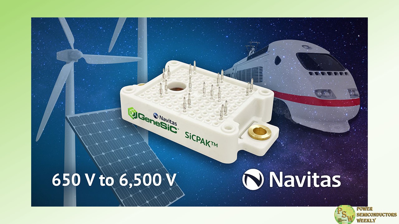
2 Min ReadNavitas Semiconductor, the only pure-play, next-generation power semiconductor company, announced their expanded portfolio into higher power markets with their leading-edge silicon carbide (SiC) power products in SiCPAK™ modules and bare die.
Target applications cover centralized and string solar inverters, energy storage systems (ESS), industrial motion, electric vehicle (EV) on-board chargers, EV roadside fast chargers, wind energy, UPS, bi-directional microgrids, DC-DC converters, and solid-state circuit breakers.
Ranging from 650 V to 6,500 V, Navitas has the widest range of SiC technology. From an original line-up of discrete packages – from 8×8 mm surface-mount QFNs to through-hole TO-247s – the GeneSiC SiCPAK is an initial, direct entry point into higher-power applications. A comprehensive power-module roadmap, with high-voltage SiC MOSFETs and MPS diodes, GaN power ICs, high-speed digital isolators and low-voltage silicon control ICs is being mapped out.
Dr. Ranbir Singh, Navitas EVP for SiC noted, “With a complete portfolio of leading-edge power, control and isolation technology, Navitas will enable customers to accelerate the transition from fossil fuels, and legacy silicon power products to new, renewable energy sources and next-generation semiconductors, with more powerful, more efficient, faster-charging systems.”
SiCPAK™ modules employ ‘press-fit’ technology to offer compact form factors for power circuits and deliver cost-effective, power-dense solutions to end users. The modules are built upon GeneSiC die that have already made a mark in terms of superior performance, reliability, and ruggedness. Examples include a SiCPAK half-bridge module, rated at 6 mOhm, 1,200 V with industry-leading trench-assisted planar-gate SiC MOSFET technology. Multiple configurations of SiC MOSFETs and MPS diodes will be available to create application-specific modules for superior system performance. The initial release will include 1,200 V-rated half-bridge modules in 6, 12, 20, and 30mOhm ratings.
Within the lead-free SiCPAK, each SiC chip is silver (Ag) sintered to the module’s substrate for superior cooling and reliability. The substrate itself is ‘direct-bonded copper’ (DBC) and manufactured using an active-metal brazing (AMB) technique on silicon-nitride (Si3N4) ceramics, ideal for power-cycling applications. This construction delivers excellent strength and flexibility, fracture resistance, and good thermal conductivity for cool, reliable, long-life operation.
For customers who prefer to make their own high-power modules, all GeneSiC MOSFET and MPS diodes are available in bare die format, with gold (Au) and aluminum (Al) top-side metalizations.
Original – Navitas Semiconductor
-
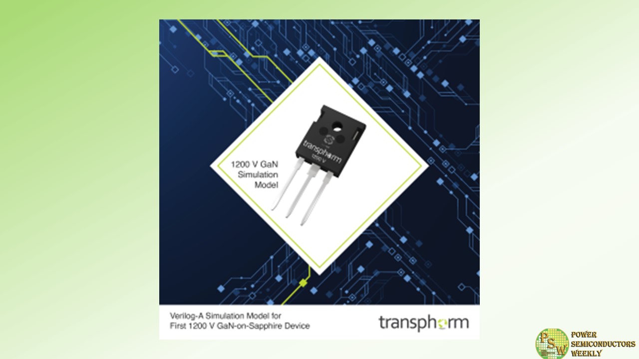
Transphorm, Inc. announced availability of its 1200 V FET simulation model and preliminary datasheet. The TP120H070WS FET is the only 1200 V GaN-on-Sapphire power semiconductor introduced to date, making its model the first of its kind. Its release indicates Transphorm’s ability to support future automotive power systems as well as three-phase power systems typically used in the broad industrial, datacom, and renewables markets. These applications will benefit from the 1200 V GaN device’s higher power density and reliability along with equal or better performance at more reasonable cost points versus alternative technologies.
Transphorm recently validated the GaN device’s higher performance ability in a 5 kW 900 V buck converter switching at 100 kHz. The 1200 V GaN device achieved 98.7% efficiency, exceeding that of a similarly rated production SiC MOSFET.
The innovative 1200 V technology also underscores Transphorm’s leadership in GaN power conversion. Vertical integration, epitaxy ownership, and patented process paired with decades of engineering expertise enable the company to bring to market the highest performing GaN device portfolio with four additional major differentiators: Manufacturability, Drivability, Designability, and Reliability.
Transphorm’s 1200 V technology is anchored in proven process and mature technology, satisfying customer confidence requirements. The GaN-on-Sapphire process is in volume production today in the LED market. Additionally, the 1200 V technology leverages the fundamentally superior, normally-off GaN platform used in Transphorm’s current device portfolio.
Key TP120H070WS device specifications include:
- 70 mΩ RDS(on)
- Normally off
- Efficient bidirectional current flow
- ± 20 Vmax gate robustness
- Low 4Vth gate drive noise immunity
- Zero QRR
- 3-lead TO-247 package
The Verilog-A device model is recommended for use with the SIMetrix Pro v8.5 Circuit Simulator. A LTSpice model is in development and will be released in Q4 2023. Simulation modeling allows for fast and efficient power system design validation while reducing design iterations, development time, and hardware investments.
The device model files and datasheet are available for download here: https://www.transphormusa.com/en/products/#models
1200 V FET samples are expected to be available by Q1 2024.
Original – Transphorm
-

As part of their strategic partnership announced earlier this year, ZF Friedrichshafen AG, a leading global technology company of next generation mobility, and Wolfspeed Inc, the global leader in Silicon Carbide technology, announced their plans to establish a joint European R&D center for Silicon Carbide power electronics in the Nuremberg Metropolitan Region.
The new joint research facility is supported by the German federal government and the regional government of Bavaria. Like the planned Wolfspeed Silicon Carbide chip factory in Ensdorf, Saarland, funding for the new center is subject to approval by the European Commission under the EU’s Important Project of Common European Interest (IPCEI) scheme, as well as antitrust authorities. The aim is to develop the two facilities to become the cornerstone of a new European Silicon Carbide technology network.
Construction will begin after IPCEI funding approval has been secured for both projects, which is expected later this year. The goal of the collaboration is to develop breakthrough innovations for Silicon Carbide systems, products, and applications, covering the full value chain from module to complete systems and thus reducing time-to-market significantly. The joint research center will target requirements in all mobility segments including consumer, commercial, agricultural, and industrial vehicles, as well as in the industrial and renewable energy markets. The collaboration aims to drive improvements such as higher efficiency, increased power density and higher performance of electrification solutions. Wolfspeed’s Silicon Carbide expertise and ZF’s access to all mobility segments allows for a fast and seamless transition of new technologies.
ZF and Wolfspeed are partnering with other leading organizations from the scientific and industrial communities to establish a comprehensive European Silicon Carbide technology network. To this end, ZF will use its membership in the European Center of Power Electronics (ECPE) and share key research results at the European level. Over time, the research center is planned to develop into an electronics and semiconductor campus.
“The research center is of outstanding importance for the energy and mobility transition in the EU and supports the strategic goals of Europe,” says Dr Holger Klein, CEO of ZF. “In addition, optimizing Silicon Carbide technology advances industrial transformation and strengthens the independence of European supply chains.”
“This research facility further strengthens our partnership with ZF and underlines our long-term commitment to turn our unique know-how from more than 35 years of experience in Silicon Carbide power electronics into state-of-the-art solutions for our industry partners,” comments Gregg Lowe, CEO of Wolfspeed Inc.
The strategic partnership links ZF, one of the world’s leading suppliers of electric drives, with Wolfspeed, the world’s most recognized specialist in Silicon Carbide technology. “This connection is unique and will lead to enormous advances in Silicon Carbide-based electrical systems and electric drives,” says ZF Board of Management member Stephan von Schuckmann. “This is made possible by the close networking of the research center and production, because fundamentally redesigned Silicon Carbide chips also require new production processes.”
Original – Wolfspeed
-

Infineon Technologies AG is diversifying its silicon carbide (SiC) supplier base and has signed a long-term agreement with Chinese SiC supplier TanKeBlue to secure additional competitive SiC sources. TanKeBlue will supply the Germany-based semiconductor manufacturer with competitive and high-quality 150-millimeter SiC wafers and boules for the manufacturing of SiC semiconductors, covering a double-digit share of the forecasted demand in the long term.
The agreement between Infineon and TanKeBlue contributes to general supply chain stability, also with regard to the growing demand for SiC semiconductor products for automotive, solar and EV charging applications and energy storage systems in the Chinese market. It will also support the rapid growth of the emerging semiconductor material SiC. The agreement will focus on 150-millimeter SiC material in the first phase, but TanKeBlue will also provide 200-millimeter SiC material to support Infineon’s transition to 200-millimeter wafer diameter.
“Infineon is significantly expanding its manufacturing capacities at its production sites in Malaysia and Austria to meet the growing demand for SiC. In order to offer the most comprehensive product range possible to our customers, Infineon is currently doubling down on its investments in SiC technology and product portfolio. In this context, we are implementing a multi-supplier and multi-country sourcing strategy to increase resilience to the benefit of our broad customer base,” said Angelique van der Burg, Chief Procurement Officer at Infineon. “TanKeBlue provides excellent material performance and we are pleased to sign a competitive agreement with them.”
“We welcome the opportunity to team up with our customer Infineon, a global leader in power semiconductors. TanKeBlue plans to continuously improve its SiC material and develop its next generation of 200-millimeter wafer technology. We value Infineon as an excellent customer in this regard,” said Yang Jian, CEO of TanKeBlue.
Infineon is currently expanding its SiC manufacturing capacity in order to achieve its target of a 30 percent global market share by the end of the decade. Infineon’s SiC manufacturing capacity will increase tenfold by 2027. A new plant in Kulim, Malaysia is scheduled to start production in 2024, adding to Infineon’s manufacturing capacities in Villach, Austria. Today, Infineon already provides SiC semiconductors to more than 3,600 automotive and industrial customers worldwide.
Original – Infineon Technologies
-
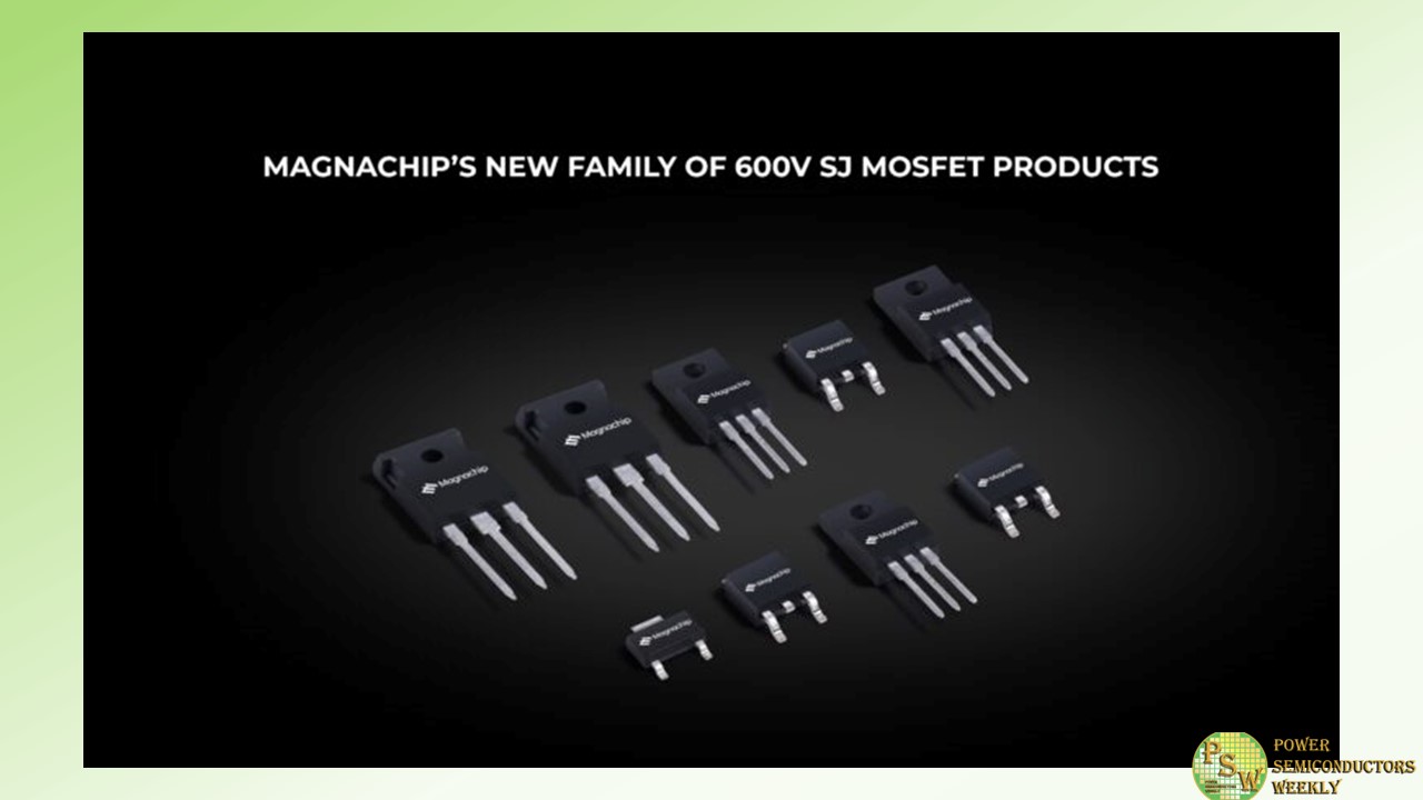
Magnachip Semiconductor Corporation (“Magnachip” or “Company”) announced that the Company has released a new family of 600V Super Junction Metal Oxide Semiconductor Field Effect Transistors (SJ MOSFETs) consisting of nine distinct products featuring proprietary design technology.
Magnachip’s proprietary design provides specific on-resistance (RSP) reduction of about 10%, and this result was achieved while maintaining the same cell-pitches of previous generation MOSFETs.
In addition, the new product family of 600V SJ MOSFETs is equipped with a fast recovery body diode. This diode technology significantly enhances system efficiency with reduced reverse recovery time (trr) and switching loss. Therefore, the figure of merit to evaluate general performance of MOSFETs was improved by more than 10% compared to the previous generation. As such, these 600V SJ MOSFETs can be used widely in industrial applications, such as solar inverters, energy storage systems, uninterruptible power supply systems, and a variety of electronics.
Among these new MOSFETs, the MMQ60R044RFTH product offers an exceptionally low RDS(on) of 44mΩ, making it an optimal choice for electric vehicle chargers and servers. Omdia, a global market research firm, estimates that the compound annual growth rates of Si MOSFET markets for hybrid & electric vehicles and servers will be 11% and 7%, respectively, from 2023 to 2026.
“Now that we have introduced these 600V SJ MOSFET products, we are aiming to unveil new 650V and 700V SJ MOSFET products with fast recovery body diode in the second half of 2023,” said YJ Kim, CEO of Magnachip. “These new MOSFETs represent a notable achievement for the Company, and we will build upon this success to deliver next-generation power solutions for rapidly changing market requirements and customer expectations.”
Original – Magnachip Semiconductor
