-
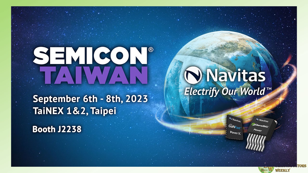
Navitas Semiconductor will reveal a new, high-performance wide bandgap power platform as part of its display at one of Asia’s most prestigious electronics exhibitions – sponsored by Navitas – SEMICON Taiwan 2023, from September 6th-8th.
Visitors will discover the latest gallium nitride (GaN) GaNFast™ power ICs integrate gallium nitride (GaN) power and drive, with control, sensing, and protection to enable faster charging, higher power density, and greater energy savings. Complementary GeneSiC™ power devices are optimized high-power, high-voltage, and high-reliability silicon carbide (SiC) solutions.
Additionally, Navitas will showcase cutting-edge, power-system platforms to dramatically accelerate customer developments, minimize time-to-market, and set new industry benchmarks in energy efficiency, power density and system cost. These system platforms include complete design collateral with fully-tested hardware, embedded software, schematics, bill-of-materials, layout, simulation and hardware test results. Examples include:
- Navitas’ CRPS185 data center power platform, that delivers a full 3,200 W of power in only 1U (40 mm) x 73.5mm x 185 mm (544 cc), achieving 5.9 W/cc, or almost 100 W/in3 power density. This is a 40% size reduction vs, the equivalent legacy silicon approach and reaches over 96.5% efficiency at 30% load, and over 96% stretching from 20% to 60% load, creating a ‘Titanium Plus’ benchmark.
- Navitas’ 6.6 kW 3-in-1 bi-directional EV on-board charger (OBC) with 3 kW DC-DC. This 96%+ efficient unit has over 50% higher power density, and with efficiency over 95%, delivers up to 16% energy savings as compared to competing solutions.
As part of SEMICON’s Power and Opto Semiconductor Forum, Navitas’ Charles Bailley, Senior Director of Business Development, will present “GaN Power ICs Increase Power Density in EV Power Systems”. The presentation is at 2pm, on September 6th, in room 402, 4F, TaiNEX 1.
“Breakthrough high efficiency, high reliability, and high power density – all from the new GaN power IC platform,” said Kevin 汪時民 Wang, Manager of Navitas Taiwan. “The new platform announcement matches SEMICON’s theme of ‘Innovating the World through Semiconductors’ and our own mission to ‘Electrify Our World™’.”
Original – Navitas Semiconductor
-
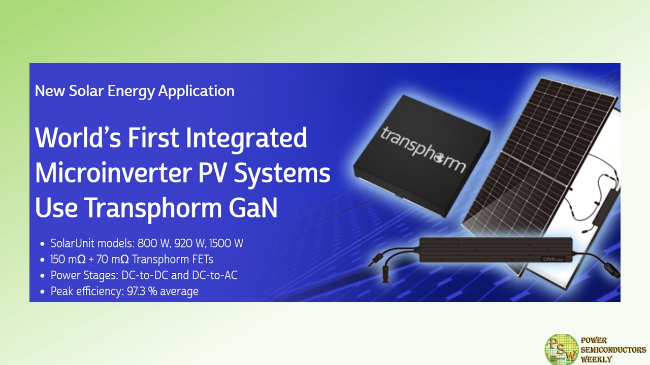
Transphorm, Inc. announced that its GaN platform powers the world’s first integrated photovoltaic (PV) systems from DAH Solar Co., Ltd. (Anhui Daheng New Energy Technology Co., LTD/subsidiary of DAH Solar). The PV systems are used in DAH Solar’s new SolarUnit product line. DAH Solar credits Transphorm’s GaN FETs with enabling it to produce smaller, lighter, and more reliable solar panel systems that also offer higher overall power generation with lower energy consumption.
The design achievements continue to demonstrate Transphorm’s One Core GaN Platform, Crossing the Power Spectrum leadership position by solidifying its value proposition in the renewables market, which currently represent a GaN TAM of more than $500M.
DAH Solar uses Transphorm’s 150 mΩ and 70 mΩ GaN FETs in the SolarUnits’ design architecture (both DC-to-DC and DC-to-AC power stages). The SolarUnits are available in three models with power outputs of 800 W, 920 W, or 1500 W and peak efficiencies of 97.16%, 97.2%, and 97.55% respectively. The GaN devices deliver higher switching frequencies and power density versus incumbent silicon solutions. Notably, the two FETs are available in PQFN88 performance packages that pair with commonly-used gate drivers—features that helped DAH Solar quicken its design time.
“We have a strong legacy of producing innovative PV products. As such, we consistently look for ways to advance our products with state-of-the-art technologies to create a better, more efficient end user experience,” said Yong Gu, GM, DAH Solar. “We view Transphorm as an authority in the field of GaN production and found their advanced GaN FETs to be the optimal devices for our new SolarUnit line. The devices are easy to design in and offer performance advantages that enable us to continue building on our legacy.”
Transphorm today supports the largest range of power conversion requirements (45 W to 10+ kW) across the widest range of power applications. The company’s FET portfolio includes 650 V and 900 V devices with 1200 V devices in development. These FETs are JEDEC and AEC-Q101 qualified, making them optimal solutions for power adapters and computer PSUs through to broad industrial UPSs and electric vehicle mobility systems.
The company’s technology innovations continue to set new benchmarks across the GaN power semiconductor industry. In parallel, they help customers bring to market new, disruptive applications in their own markets—such as DAH Solar’s PV systems.
These achievements are due to Transphorm’s normally-off SuperGaN® platform, which uses the cascode d-mode configuration to harness GaN’s intrinsic advantages. The superior physics of this high performance GaN platform design delivers competitively unmatched benefits such as easier drivability, easier designability, higher reliability, and greater manufacturability.
“The value Transphorm’s GaN platform brings to a variety of applications continues to be demonstrated by market leaders like DAH Solar,” Kenny Yim, Vice President of Asia Sales, Transphorm. “Solar inverters as well as other high-power applications require highly reliable, high performing power semiconductors that can withstand decades of operation in harsh environments.
Using Transphorm’s SuperGaN technology helps reduce power loss thereby minimizing thermal stress on other designed-in components. That’s a phenomenal achievement over alternative GaN and Silicon solutions underscoring the benefits our GaN brings to next generation power systems.”
Original – Transphorm
-
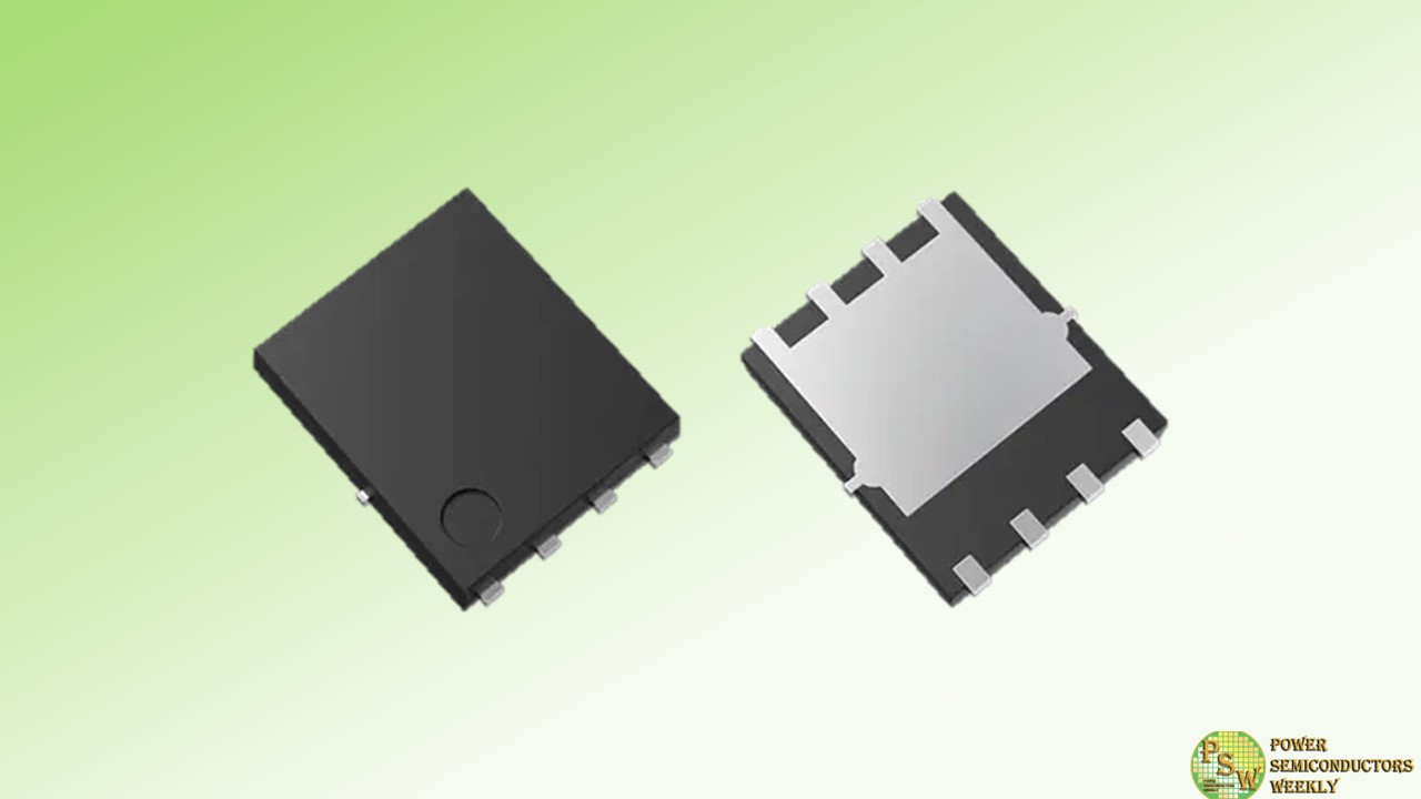
Toshiba Electronic Devices & Storage Corporation has launched three 80 V N-channel power MOSFET products that use its latest generation process “U-MOSX-H series” and are suitable for switching power supplies for industrial equipment—used for such as data centers and communication base stations—and expanded the lineup.
The new products use the surface mount type SOP Advance(N) package, and their drain-source On-resistance (max) is 3 mΩ for “TPH3R008QM”, 6 mΩ for “TPH6R008QM”, and 8.8 mΩ for “TPH8R808QM”.
The new products have reduced the figure of merits (FOMs: expressed as On-resistance × charge characteristics.) In case of TPH3R008QM, it has reduced its FOMs, drain-source On-resistance × total gate charge by approximately 48 %, drain-source On-resistance × gate switch charge by approximately 16 %, and drain-source On-resistance × output charge by approximately 33 %, compared to Toshiba’s existing product TPH4R008NH. This contributes to lowering power consumption of equipment.
Toshiba is expanding its lineup of products to help cut equipment power consumption.
Applications
- Switching power supplies (high efficiency AC-DC converters, high efficiency DC-DC converters, etc.)
- Motor control equipment (motor drives, etc.)
Features
- Latest generation process U-MOSX-H series
- Low On-resistance:
TPH3R008QM RDS(ON)=3 mΩ (max) (VGS=10 V)
TPH6R008QM RDS(ON)=6 mΩ (max) (VGS=10 V)
TPH8R808QM RDS(ON)=8.8 mΩ (max) (VGS=10 V) - High channel temperature: Tch (max)=175 °C
Original – Toshiba
-

onsemi announced that Christina Lampe-Önnerud was appointed to its board of directors, effective September 1, 2023.
Lampe-Önnerud is a highly regarded founder and business leader, having served as chief executive officer of two separate companies, and is also considered an expert in the energy storage space. Among her unique global experience, she has been active in multiple domestic and international government delegations as an authority on energy technologies.
As a two-time World Economic Forum (WEF) Technology Pioneer, who has served as co-chairman of the WEF Global Future Council on Energy, she continues to be engaged in multiple initiatives throughout the United States, Europe and Asia.
“Christina brings a wealth of experience as a pioneer and innovator in battery technologies designed to improve energy storage and power consumption,” said Alan Campbell, chair of onsemi’s board of directors. “Her work, values and passion are well-aligned with onsemi’s strategic priorities focused on delivering innovative technologies for the automotive and industrial end-markets that deliver a sustainable future, and we look forward to her invaluable contributions to the board.”
“onsemi’s ambition to deliver industry-leading power and sensing technologies that will transform our world’s energy usage is where I’ve dedicated my life’s work,” said Christina Lampe-Önnerud. “It is an exciting time to be joining the board to support the leadership team as they continue to execute on the strategy and drive long-term shareholder value and sustainable results.”
Lampe-Önnerud holds more than 80 patents on designs, products, devices, components, materials, and processes. She has over 25 technical publications in scientific journals focusing on science and thought leadership. She is also frequently tapped as an expert commentator in media interviews and regularly speaks at government and industry conferences on power and energy issues.
Lampe-Önnerud received both a Bachelor of Science degree in chemistry and calculus and a Ph.D. in inorganic chemistry from Uppsala University, Sweden. She completed her post-doctorate at Massachusetts Institute of Technology, where she serves on the Visiting Committee. In 2022, she was honored with the King’s Medal, one of Sweden’s most prestigious awards, for her work in producing safe, low-cost, high-performance lithium-ion batteries.
Original – onsemi
-
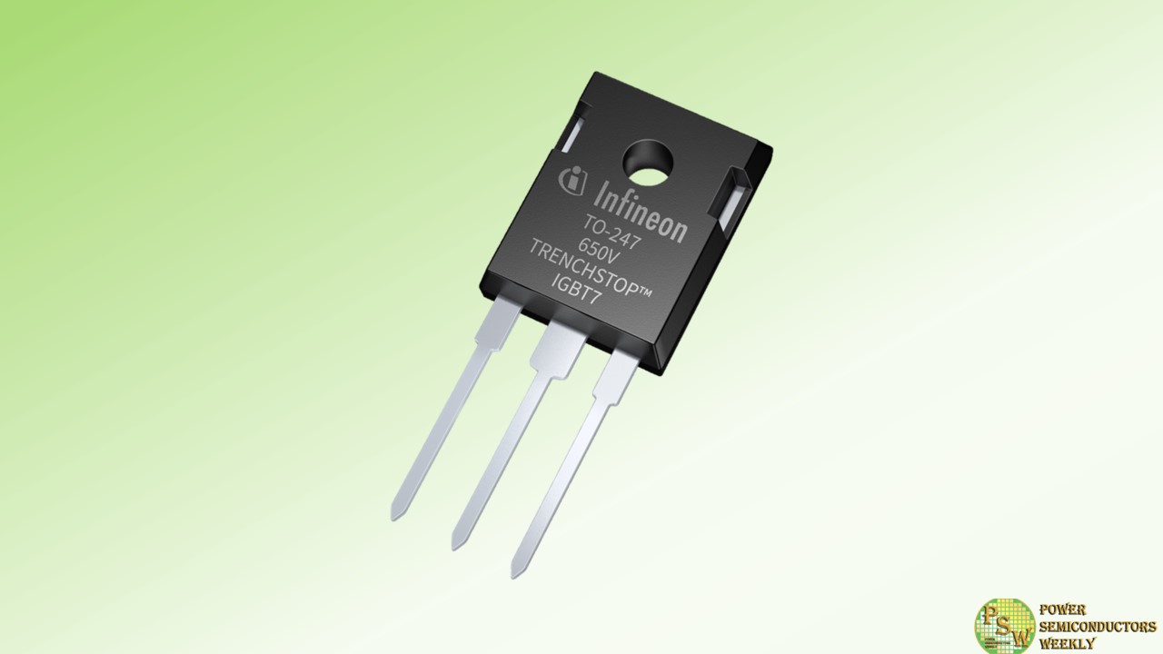
Infineon Technologies AG expands its 7th generation TRENCHSTOP™ IGBT family with the discrete 650 V IGBT7 H7 variant. The devices feature a cutting-edge EC7 co-packed diode with an advanced emitter-controlled design, coupled with high-speed technology to address the escalating need for environmentally conscious and highly efficient power solutions.
Using the latest micro-pattern trench technology, the TRENCHSTOP IGBT7 H7 offers excellent control and performance, resulting in significant loss reduction, improved efficiency and higher power density. As a result, the device is ideal for various applications such as string inverters, energy storage systems (ESS), electric vehicle charging applications, and traditional applications such as industrial UPS and welding.
In a discrete package, the 650 V TRENCHSTOP IGBT7 H7 can deliver up to 150 A. The portfolio includes variants from 40 A to 150 A, offered in four different package types: TO-247-3 HCC, TO-247-4, TO-247-3 Plus and TO-247-4 Plus. The TO-247-3 HCC variant of the TRENCHSTOP IGBT 7 H7 features a high creepage distance.
For improved performance, the TO-247 4-pin packages (standard: IKZA, Plus: IKY) are particularly well suited, as they not only reduce switching losses, but also offer additional benefits such as lower voltage overshoot, minimized conduction losses and the lowest reverse current loss. With these features, the TRENCHSTOP IGBT 7 H7 simplifies the design and minimizes the need to connect devices in parallel.
In addition, the 650 V TRENCHSTOP IGBT 7 H7 features robust moisture resistance for reliable operation in harsh environments. The device is qualified for industrial use according to the relevant tests of JEDEC47/20/22, especially HV-H3TRB, making it well suited for outdoor applications.
Designed to meet the demand for green and efficient power applications, the IGBT offers significant improvements over the previous generations. As a result, the TRENCHSTOP IGBT 7 H7 is the ideal complement for the NPC1 topology often used in applications such as solar and ESS.
Original – Infineon Technologies
-

CVD Equipment Corporation appointed Dr. Ashraf Lotfi to its Board of Directors. The Board of Directors also approved an expansion of the number of directors from the current level of five to six.
“We are delighted that Dr. Lotfi has agreed to join our Board,” said Lawrence J. Waldman, Chairman of CVD Equipment Corporation’s Board of Directors. “His extensive semiconductor and power electronics device industry expertise, and proven track record of bringing innovative technologies to market, will be invaluable as we execute our core strategy focused on the electrification of everything.”
Dr. Lotfi is currently a venture partner with Deep Sciences Ventures and serves on the board of Lotus Microsystems, ApS. Dr. Lotfi previously served as Vice President and a Fellow at Intel Corporation. Prior to Intel, he was Power Chief Technology Officer for Altera Corporation serving its Enpirion Power Business as well as the broader Field Programmable Gate Array community. Altera was acquired by Intel in 2015. Prior to Altera, he served as President and Chief Executive Officer of Enpirion, Inc., which he founded in 2002.
From Enpirion’s inception, Dr. Lotfi led its strategic direction with a unique industry‐first vision to create the ultimate power converter‐on‐chip creating ubiquitous DC‐DC conversion at the silicon level. In 2013, he led Enpirion’s merger into Altera to realize his vision of highly integrated power management closely coupled to leading‐edge digital silicon loads. Prior to founding Enpirion, he was Director of Advanced Power Research at Bell Laboratories.
Manny Lakios, President and CEO of CVD Equipment Corporation, also commented, “We are very pleased to welcome Dr. Lotfi to our Board of Directors. His in-depth knowledge of the power electronics market and his track record of scaling the Enpirion Power Business will allow him to immediately contribute to our management team and Board of Directors as we pursue the pipeline of customer opportunities in our key strategic markets of high-power electronics, battery materials/energy storage and aerospace and defense.”
Dr. Lotfi stated, “I am very delighted to join CVD Equipment Corporation. Its long history and solid IP capabilities, particularly in silicon carbide, the essential enabling technology for electrification, form a strong basis for continued growth and participation in critical parts of vital applications and growth markets.”
Original – CVD Equipment
-

MACOM Technology Solutions Holdings, Inc. announced that it has entered into a definitive agreement to acquire the radio frequency business of Wolfspeed, Inc. The RF Business includes a portfolio of Gallium Nitride (“GaN”) on Silicon Carbide (“SiC”) products used in high performance RF and microwave applications.
The business services a broad customer base of leading aerospace, defense, industrial and telecommunications customers and most recently generated annualized revenues of approximately $150 million. The acquisition is expected to be immediately accretive to MACOM’s non-GAAP earnings.
“We are excited to acquire Wolfspeed’s RF Business and look forward to welcoming its employees to MACOM,” stated Stephen G. Daly, President and Chief Executive Officer, MACOM. “The RF team’s engineering capabilities, technology and products are a perfect fit with MACOM and our strategy.”
The acquisition includes a 100mm GaN wafer fabrication facility in Research Triangle Park, North Carolina (the “RTP Fab”) with operations conveying to MACOM approximately two years following the closing and Wolfspeed’s relocation of certain production equipment.
The acquisition also includes design teams and associated product development assets in Arizona, California and North Carolina, as well as back-end production capabilities in California and Malaysia. In addition, MACOM will be assigned or licensed a robust intellectual property portfolio including over 1,400 patents associated with the RF Business.
The RF Business will be acquired for $125 million, including $75 million cash paid at closing and $50 million of MACOM common stock issued with certain restrictions. A workforce of approximately 280 employees is expected to join MACOM at closing, with additional employees joining when the RTP Fab conveys.
Closing of the transaction is subject to the expiration of a waiting period under the Hart-Scott-Rodino Antitrust Improvements Act of 1976 and other closing conditions and is expected to occur in the second half of calendar year 2023.
Original – MACOM Technology Solutions
-

The University of Arkansas celebrated an important milestone with the groundbreaking on a building that Chancellor Charles Robinson suggested might someday rival the U of A’s most iconic structure, Old Main, in significance to the university and the state of Arkansas.
Robinson and other university leaders, including University of Arkansas System President Don Bobbitt and members of the U of A System Board of Trustees, as well as researchers and industry leaders, gathered at the Arkansas Research and Technology Park in South Fayetteville to celebrate construction of the national Multi-User Silicon Carbide Research and Fabrication Facility, or MUSiC.
The new semiconductor research and fabrication facility will produce microelectronic chips made with silicon carbide, a powerful semiconductor that outperforms basic silicon in several critical ways. The facility will enable the federal government – via national laboratories – businesses of all sizes, and other universities to prototype with silicon carbide, a capability that does not presently exist elsewhere in the U.S.
Work at the facility will bridge the gap between traditional university research and the needs of private industry and will accelerate technological advancement by providing a single location where chips can go from developmental research to prototyping, testing and fabrication.
“This fills a gap for our nation, allowing companies, national laboratories and universities around the nation to develop the low-volume prototypes that go from their labs to fab, ultimately scaling up to the high-volume manufacturing…” said Alan Mantooth, Distinguished Professor of electrical engineering and principal investigator for the MUSiC facility. “We fill that gap. And there’s no other place like it in the world. This is the only place that will be able to do that with silicon carbide.”
The 18,660 square-foot facility, located next to the National Center for Reliable Electrical Power Transmission at the research and technology park, will address obstacles to U.S. competitiveness in the development of silicon-carbide electronics used in a wide range of electronic devices, circuits and other consumer applications. The building will feature approximately 8,000 square feet of clean rooms for fabrication and testing.
Education and training within the facility will also accelerate workforce development, helping supply the next generation of engineers and technicians in semiconductor manufacturing, which Mantooth and other leaders have said is critical for bringing semiconductor manufacturing back to the U.S., after it was offshored in the late 1990s and early 2000s.
“This is truly a special day in the life of the University of Arkansas,” said Robinson. “This building, it really doesn’t need to be hyped. It is a very important building, and you just know it, important for our university, important for our state, important for our nation.”
Robinson invoked another groundbreaking, that of Old Main, the university’s oldest and best known structure, which the university celebrated Aug. 17, 1873, almost exactly 150 years ago.
“I took that 150th anniversary of the groundbreaking as a good sign that we are moving in a timely way,” Robinson said, “doing important work in establishing this building.”
Friday’s groundbreaking occurred a day after the university and the Arkansas Department of Commerce hosted the CHIPS AMERICA Summit, an event in which research, industry and governmental leaders discussed semiconductor-related opportunities resulting from the CHIPS (Creating Helpful Incentives to Produce Semiconductors) and Science Act passed by Congress in 2022. The event featured Adrienne Elrod, director of external and government affairs for the U.S. Department of Commerce’s CHIPS Program Office, U.S. Rep. Steve Womack and Arkansas Secretary of Commerce Hugh McDonald.
During the summit, Elrod stated that prior to the coronavirus pandemic, 90% of the world’s leading-edge chips were manufactured at one facility in Taiwan. The federal government prioritized the onshoring of this critical technology as a result of manufacturing and production shortages of essential computer chips during the pandemic.
“If America is going to compete and lead the world over the next century, we must invest in our technology and manufacturing,” Elrod said. “We want to make sure, at the very least, that we have two new large-scale clusters of leading- edge fabs created (in the United States).”
As Mantooth mentioned, the University of Arkansas can contribute to this effort on a fundamental level and is uniquely positioned to take advantage of opportunities offered by the CHIPS and Science Act, which is providing approximately $280 billion in funding to stimulate domestic research and manufacturing of semiconductors.
“The university is leaning forward and has now secured funding for projects important to microelectronics research and development,” Womack said during Thursday’s summit. “The university has positioned itself, as I say often, to be the preeminent university research location for microelectronics. … I am grateful for the bright minds at the University of Arkansas with a proven track record of success who will make this happen.”
Original – University of Arkansas
-

Renesas Electronics Corporation announced a change in its largest major shareholder, which will become effective as of August 23, 2023.
Renesas received notification from INCJ, Ltd. on August 18, 2023, that it will sell a portion of its holdings in Renesas. Effective August 23, 2023, when the stock transfer is completed, INCJ, Ltd. will no longer be the largest major shareholder of Renesas.
Name INCJ, Ltd. Location 1-3-1, Toranomon, Minato-ku,Tokyo, Japan Names and titles of representatives Chairman and CEO: Toshiyuki ShigaPresident and COO: Mikihide Katsumata Main Business Specific business activity support and other work stipulated in the current Act on Strengthening Industrial Competitiveness as of September 21, 2018 Amount of capital 500 million yen Number of voting rights(Number of shares held) Ratio to the number of voting rights held by all shareholders Shareholder ranking Before the change
(June 30)1,838,127(183,812,775 shares) 10.41% 2nd After the change 1,749,121(174,912,175 shares) 9.90% 2nd Note 1. “Ratio to the number of voting rights held by all shareholders” before the change is calculated based on the number of voting rights of all shareholders (17,650,540) as of June 30, 2023.
Note 2. “Ratio to the number of voting rights held by all shareholders” after the change is calculated based on the number of voting rights of all shareholders as of June 30, 2023 (17,650,540) plus the number of voting rights (3,983) pertaining to the treasury shares subsequently disposed under Renesas’ stock compensation plan, ending in a total voting rights of 17,654,523 (but not including treasury stock disposed after August 1, 2023).
Note 3. While The Master Trust Bank of Japan, Ltd. (Trust Account) is ranked first among large shareholders before and after the change, it does not fall under the category of major shareholder or the largest shareholder as part of the major shareholder group.
Original – Renesas Electronics
-

Toshiba Electronic Devices & Storage Corporation has launched two automotive 40V N-channel power MOSFETs, “XPJR6604PB” and “XPJ1R004PB,” that use Toshiba’s new S-TOGL™ (Small Transistor Outline Gull-wing Leads) package with U-MOS IX-H process chips. Volume shipments start today.
Safety-critical applications like autonomous driving systems ensure reliability through redundant design, with the result that they integrate more devices and require more mounting space than standard systems. Accordingly, advancing size reductions in automotive equipment requires power MOSFETs that can be mounted at high current densities.
XPJR6604PB and XPJ1R004PB use Toshiba’s new S-TOGL™ package (7.0mm×8.44mm) which features a post-less structure unifying the source connective part and outer leads. A multi-pin structure for the source leads decreases package resistance.
The combination of the S-TOGL™ package and Toshiba’s U-MOS IX-H process achieve a significant On-resistance reduction of 11% against Toshiba’s TO-220SM (W) package product, which has the same thermal resistance characteristics. The new package also cuts the required mounting area by approximately 55% against the TO-220SM(W) package.
On top of this, the 200A drain current rating of the new package is higher than Toshiba’s similarly sized DPAK + package (6.5mm×9.5mm), enabling high current flow. Overall, the S-TOGL™ package realizes high-density and compact layouts, reduces the size of automotive equipment, and contributes to high heat dissipation.
Since automotive equipment is used in extreme temperature environments, the reliability of surface mounting solder joints is a critical consideration. The S-TOGL™ package uses gull-wing leads that reduce mounting stress, improving the reliability of the solder joint.
Assuming that multiple devices will be connected in parallel for applications requiring higher-current operation, Toshiba supports grouping shipment for the new products, in which the gate threshold voltage is used for grouping. This allows designs using product groups with small characteristic variation.
Toshiba will continue to expand its product line-up of power semiconductor products and contribute to the realization of carbon neutrality with more user-friendly, high-performance power devices.
Features:
- New S-TOGL™ package: 7.0mm×8.44mm (typ.)
- Large drain current rating:
XPJR6604PB: ID=200A
XPJ1R004PB: ID=160A - AEC-Q101 qualified
- IATF 16949/PPAP available[4]
- Low On-resistance:
XPJR6604PB: RDS(ON)=0.53mΩ (typ.) (VGS=10V)
XPJ1R004PB: RDS(ON)=0.8mΩ (typ.) (VGS=10V)
Original – Toshiba
