-

The U.S. Department of Energy (DOE)’s Advanced Materials and Manufacturing Technologies Office (AMMTO) announced renewed funding for PowerAmerica, DOE’s first Clean Energy Manufacturing Innovation Institute. PowerAmerica will receive an initial $8 million, with potential funding across four more fiscal years to follow, to continue advancing domestic manufacturing of next-generation WBG semiconductors for power electronics to aid economy-wide decarbonization and electrification.
WBG semiconductors use cutting-edge materials that enable power electronics that are used in a range of applications—including industrial equipment, data centers, consumer devices, electric vehicles, and more. Silicon carbide (SiC) and gallium nitride (GaN) WBG semiconductor technology makes the power electronic modules significantly more powerful and energy efficient than those made from conventional semiconductor materials, namely silicon. These high-performance power electronics can increase electric vehicle driving range; help integrate renewable energy into the electric grid; and lead to significant energy savings.
“The work PowerAmerica—and its 82 member organizations spanning industry, academia, and national labs—is doing to galvanize commercialization of high-performance power electronics is invaluable to our clean energy future,” said AMMTO Director Chris Saldaña. “PowerAmerica has catalyzed an innovation ecosystem that touches nearly every sector up and down each supply chain.”
Raleigh-based PowerAmerica commercialized more than 10 WBG technologies over five years. To date, 40 percent of PowerAmerica’s 60 projects have reached or are set to reach commercial status.
Not only is PowerAmerica innovating semiconductors that surpass operational limitations of traditional silicon-based designs, but it also focuses on training the future workforce of America’s manufacturing sector through its strong education and workforce development (EWD) program. Since launching in 2014, PowerAmerica has trained more than; 400 masters and PhD students, 300 short course attendees, 1,800 tutorial participants, and 9,000 K-12 students in STEM programs, including 2,000 participants of hands-on trainings. These numbers are particularly important in addressing the acute workforce shortage the power electronics industry faces, and scaling up PowerAmerica’s existing EWD program is a proposed focus of the new federal funding.
This federal funding builds upon initial federal funding of $70 million, in addition to $81 million in cost share from its member partners, for a total of $151 million.
PowerAmerica is one of seven Clean Energy Manufacturing Innovation Institutes supported by two of DOE’s Energy Efficiency and Renewable Energy program offices: the Advanced Materials and Manufacturing Technologies Office (AMMTO) and Industrial Efficiency and Decarbonization Office (IEDO). In addition, PowerAmerica is one of the 16 member institutes of Manufacturing USA™, a national network of manufacturing innovation institutes created to secure U.S. global leadership in advanced manufacturing through large-scale public-private collaboration on technology, supply chain, and education and workforce development.
Original – DOE
-

The rapid growth of technology over the past century brought us as many advantages as many disadvantages including the accelerating global warming with its dramatic consequences we face every day in various parts of the Earth. So far no one found a solution how to stop this process, but there are many solutions how to slow it down.
Today we try to respond to this challenge with carbon neutrality initiatives launched in many countries across the globe. And one of the major steps in this green society program is the electrification of passenger and commercial vehicles.
Right now, companies have various approaches to vehicle electrification including mild-hybrid electric vehicles MHEV, full hybrid electric vehicles HEV, plug-in hybrid electric vehicles PHEV, battery electric vehicles BEV, and fuel-cell electric vehicle FCEV. What some time ago seemed like a big step forward is a reality we live in now.
And to make this dream come true became possible with the help of power semiconductors. For a long time, semiconductors were used in the automotive industry, and the evolution of power semiconductor materials pushed the transition to the electrification of vehicles. Electric vehicles’ performance and cost depend on the technical level of the motor control system.
Previously, silicon (Si) IGBT modules served as the heart of electronic control systems with their relatively high switching speed and low conduction loss. But with the growth of silicon carbide (SiC) technology, EVs step into the new era of electrification.
Silicon-based semiconductors have been dominating the market for many decades. No wonder, several generations of power electronics engineers were passing their knowledge and experience working with silicon semiconductors. Through time they have short-listed their preferred solutions produced by several companies.
Based on the current requirements for the improvement of battery life and dynamic performance of electric passenger and commercial vehicles, higher efficiency, and fewer parts and materials are required to further improve the power density of inverters and electric drive assemblies. All this becomes possible with the transition from Si to SiC power devices. But when it comes to the all-new silicon carbide semiconductors and the rapidly growing EV industry, many face difficulties to make the right choice of the silicon carbide devices available in the market.
Recently I launched a poll to understand what is most important for EV companies when choosing a supplier of SiC power devices. Power electronics engineers from the semiconductor and automotive industries shared their experience and unanimously confirmed that the performance of the power devices plays a crucial role when choosing a supplier. The poll results are:
- Performance/characteristics – 66%
- Price – 16%
- Lead time – 9%
- Brand – 9%
Based on the results it is clear that for the EV market today characteristics of SiC power devices and price play the most important role. After all, consumers want high performance and reliability at affordable prices.
Nowadays SiC is still more expensive than Si. However, the prices have dropped a lot in the past decade, and the growing number of SiC fabs promises to drop the price in the future. Fingers crossed, in the nearest future, the dream of the consumers for the high-performance, reliable, and affordable EV will come true.
-
The electrification of the transportation system is advancing continuously. In addition to passenger cars, 2- and 3-wheelers as well as light vehicles are increasingly being electrified. Therefore, the automotive market for Electronic Control Units (ECUs) powered by 24 V-72 V is expected to keep growing in the coming years.
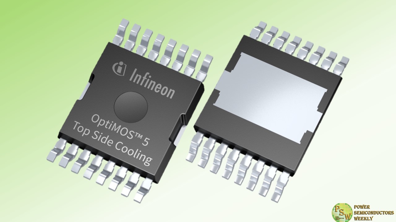
To address this development, Infineon Technologies AG is complementing its OptiMOS™ 5 portfolio of automotive MOSFETs in the 60 V and 120 V range with new products in the high power packages TOLL, TOLG and TOLT. They are offering a compact form factor with very good thermal performance combined with excellent switching behavior.
The six new products offer a narrowed gate threshold voltage (V GS(th)) enabling designs with parallel MOSFETs for increased output power capability. The IAUTN06S5N008, IAUTN06S5N008G and IAUTN06S5N008T are 60 V MOSFETs, and the IAUTN12S5N017, IAUTN12S5N018G and IAUTN12S5N018T are 120 V MOSFETs.
The on resistance (R DS(on)) ranges from 1.7 mΩ to 1.8 mΩ for the 120 V MOSFETs and is 0.8 mΩ for the 60 V MOSFETs. This makes the 60V MOSFETs perfectly suited for high power 24 V supplied CAV applications or for HV-LV DCDC converters in xEVs. The 120 V MOSFETs are used in 48 V – 72 V supplied traction inverters for 2- or 3-wheelers and light electric vehicles.
Original – Infineon Technologies
-
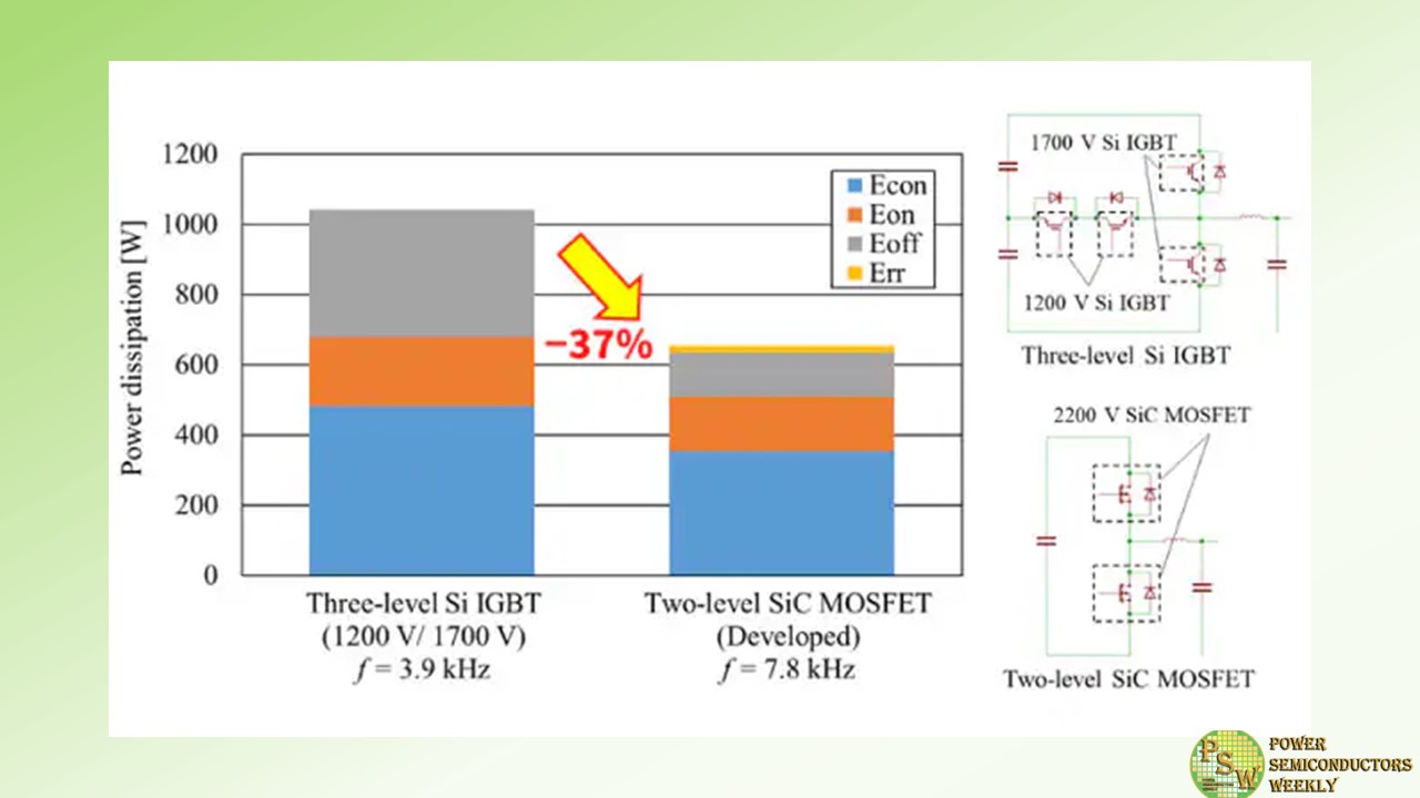
Toshiba Electronic Devices & Storage Corporation has developed 2200 V silicon carbide (SiC) metal oxide semiconductor field effect transistors (MOSFETs) for photovoltaic (PV) inverters. A two-level inverter with the new devices realized higher frequency operation and lower power loss than a conventional three-level silicon (Si) insulated gate bipolar transistor (IGBT) inverter. The new MOSFETs also contribute to simplification of inverter systems and reductions in their size and weight.
Three-level inverters enjoy the advantage of low switching losses because the voltage applied to switching devices in the inverters during off-state is half the line voltage. Against this, two-level inverters have fewer switching modules than three-level inverters, realizing a simpler, smaller, and lighter system. However, they require semiconductors with higher breakdown voltage, as the applied voltage is equal to the line voltage. Also, demand for semiconductors with both low loss and high breakdown voltage is growing as 1500 V DC line voltage systems are introduced in photovoltaic and other renewable energy markets.
Toshiba Electronic Devices & Storage Corporation has developed 2200 V Schottky barrier diode (SBD)-embedded SiC MOSFETs for two-level inverters in 1500 V DC voltage systems. The impurity concentration and thickness of the drift layer has been optimized to maintain the same relationship between the on-resistance and the breakdown voltage as our existing products, and also to achieve high resistance to cosmic rays, a requirement for PV systems. It has also been confirmed that embedding SBDs clamped parasitic PN junctions between the p-base regions and the n-drift layer secure high reliability in reverse conduction.
Switching energy loss for the developed all-SiC module is far lower than for the Si module (Si IGBTs + Si fast recovery diodes) with the same 2000 V rated voltage class. Estimates of inverter power dissipation found that the developed SiC module achieves higher frequency operation twice that of a conventional Si IGBT, as well as a 37% lower loss for the two-level SiC inverter against the three-level Si inverter. The higher frequency operation enables downsizing and weight reduction of other system components, such as heat sinks and filters.
Original – Toshiba
-

The University of Arkansas has taken the next step to becoming a national leader in the United States’ semiconductor economy. Semiconductors, such as silicon, are essential materials in most electronic devices and advance performance in fields such as healthcare, national defense, computing and transportation.
This August, the university began construction on the national Multi-User Silicon Carbide Research and Fabrication Facility, or MUSiC. Capable of silicon or silicon carbide chip fabrication, this new semiconductor research and fabrication facility will enable the government, businesses of all sizes, and universities to prototype in silicon carbide, introducing a capability that does not presently exist in the U.S.
This unique facility will offer low-volume prototyping for high-volume manufacturing, bridging the gap between traditional university research and the needs of private industry. This will accelerate both workforce development and technological advancement in semiconductors by providing a single location where chips can be go from developmental research to prototyping, testing and fabrication.
Alan Mantooth, Distinguished Professor of electrical engineering at the U of A, is principal investigator for MUSiC. He stated that with MUSiC, the university could “begin training the next generation at a variety of degree levels to provide well-trained and educated talent for onshoring semiconductor manufacturing that domestic suppliers offshored in the late 90s and early 2000s. Our training will be equally applicable to silicon and silicon carbide and other materials.”
Construction coincides with the CHIPS America Summit on Aug. 17, an invitation-only event for research, industry and governmental leaders from across the nation to discuss CHIPS and Science Act semiconductor-related opportunities and the ways in which the U of A and the State of Arkansas are uniquely positioned to lead.
The summit will feature Director of External and Government Affairs for the U.S Department of Commerce’s CHIPS Program Office, Adrienne Elrod. U.S. Representative Steve Womack and Arkansas Secretary of Commerce Hugh McDonald will also participate.
In addition to the MUSiC facility, the U of A is also home to the first Energy Frontier Research Center in Arkansas, as part of a team of researchers who received $10.35 million from the U.S. Department of Energy. The Center for Manipulation of Atomic Ordering for Manufacturing Semiconductors is dedicated to investigating the formation of atomic orders in semiconductor alloys and their effects on various physical properties. This research program will enable reliable, cost-effective and transformative manufacturing of semiconductors.
Researchers at the U of A previously established the MonArk NSF Quantum Foundry to accelerate the development of quantum materials and devices. In collaboration with Montana State University, and other member universities, the foundry supports the study of 2-D materials — consisting of a single layer of bonded atoms — by aiding researchers and facilitating the exchange of ideas across academia and industry. The project leads the fabrication of 2-D material quantum devices and their characterization, using low-temperature electronic transport and optoelectronic techniques.
The U of A’s existing and expanding research foundation means it’s uniquely positioned to take advantage of the recent CHIPS (Creating Helpful Incentives to Produce Semiconductors) and Science Act, which is providing approximately $280 billion in funding to stimulate domestic research and manufacturing of semiconductors.
As a result of manufacturing and production shortages of essential computer chips during the pandemic, which are overwhelmingly manufactured overseas, the federal government has prioritized the onshoring of this critical technology.
About the University of Arkansas: As Arkansas’ flagship institution, the U of A provides an internationally competitive education in more than 200 academic programs. Founded in 1871, the U of A contributes more than $2.2 billion to Arkansas’ economy through the teaching of new knowledge and skills, entrepreneurship and job development, discovery through research and creative activity while also providing training for professional disciplines.
The Carnegie Foundation classifies the U of A among the few U.S. colleges and universities with the highest level of research activity. U.S. News & World Report ranks the U of A among the top public universities in the nation. See how the U of A works to build a better world at Arkansas Research and Economic Development News.
The national Multi-User Silicon Carbide Research and Fabrication Facility, or MUSiC, will provide opportunities for the government and business of all sizes, and universities to prototype in silicon carbide, introducting a capability that does not currently exist in the U.S.
Original – University of Arkansas
-

Transphorm, Inc. announced it has demonstrated up to 5 microsecond short circuit withstand time (SCWT) on a GaN power transistor with a patented technology. The achievement is the first of its kind on record, marking an important milestone for the industry as a whole. It proves Transphorm GaN’s ability to meet the required short circuit capabilities of rugged power inverters such as servo motors, industrial motors, and automotive powertrains served traditionally by silicon IGBTs or silicon carbide (SiC) MOSFETs— an over $3 billion GaN TAM over the next 5 years.
The demonstration was developed with support from Yaskawa Electric Corporation, a long-term strategic partner of Transphorm’s and a global leader in low and medium voltage drives, servo systems, machine controllers, and industrial robots. This makes GaN a highly attractive power conversion technology for servo systems, as it allows for higher efficiency and reduced size compared to incumbent solutions.
To do that, GaN must pass stringent robustness tests—of which, short-circuit survivability is the most challenging. In case of short-circuit faults, the device must survive extreme conditions with both high current and high voltage. The system can take up to a few microseconds to detect the fault and shut down the operations. During this time, the device must withstand the fault on its own.
“If a power semiconductor device cannot survive short-circuit events, the system itself may fail. There was a strong perception that GaN power transistors could not meet the short circuit requirements needed for heavy-duty power applications such as ours,” said Motoshige Maeda, Department Manager of Fundamental R&D Management Department, Corporate Technology Division, Yaskawa. “Having worked with Transphorm for many years, we believed that perception to be unfounded and have been proven right today. We’re excited about what their team has accomplished and look forward to demonstrating how this new GaN feature can benefit our designs.”
The short-circuit technology has been demonstrated on a newly designed 15 mΩ 650 V GaN device. Notably, that device reaches a peak efficiency of 99.2% and a maximum power of 12 kW in hard-switching conditions at 50 kHz. The device demonstrated not only performance, but also reliability, passing high-temperature high-voltage stress requirements.
“Standard GaN devices can withstand short-circuit for only a few hundredths of nanoseconds, which is too short for fault detection and safe shut-down. However, with our cascode architecture and key patented technology, we were able to demonstrate short-circuit withstand time up to 5 microseconds with no additional external components, thus retaining low cost and high performance,” said Umesh Mishra, CTO and Co-Founder, Transphorm.
“We understand the demands of high-power, high-performance inverter systems. We have a long history of strong innovation, and we’re proud to say that experience helped us bring GaN to the next level. This is yet another validation of Transphorm’s global leadership in high voltage GaN robustness and reliability and will be a gamechanger for GaN in motor drives and other high-power systems.”
The full description explaining the SCWT achievement, the demonstration analysis, and more is expected to be presented at a major power electronics conference next year.
Original – Transphorm
-
TSMC, Robert Bosch GmbH, Infineon Technologies AG, and NXP Semiconductors N.V. announced a plan to jointly invest in European Semiconductor Manufacturing Company (ESMC) GmbH, in Dresden, Germany to provide advanced semiconductor manufacturing services. ESMC marks a significant step towards construction of a 300 mm fab to support the future capacity needs of the fast-growing automotive and industrial sectors, with the final investment decision pending confirmation of the level of public funding for this project. The project is planned under the framework of the European Chips Act.
The planned fab is expected to have a monthly production capacity of 40,000 300 mm (12-inch) wafers on TSMC’s 28/22 nanometer planar CMOS and 16/12 nanometer FinFET process technology, further strengthening Europe’s semiconductor manufacturing ecosystem with advanced FinFET transistor technology and creating about 2,000 direct high-tech professional jobs. ESMC aims to begin construction of the fab in the second half of 2024 with production targeted to begin by the end of 2027.
The planned joint venture will be 70 percent owned by TSMC, with Bosch, Infineon, and NXP each holding 10 percent equity stake, subject to regulatory approvals and other conditions. Total investments are expected to exceed 10 billion euros consisting of equity injection, debt borrowing, and strong support from the European Union and German government. The fab will be operated by TSMC.
“This investment in Dresden demonstrates TSMC’s commitment to serving our customers’ strategic capacity and technology needs, and we are excited at this opportunity to deepen our long-standing partnership with Bosch, Infineon, and NXP,” said Dr. CC Wei, Chief Executive Officer of TSMC. “Europe is a highly promising place for semiconductor innovation, particularly in the automotive and industrial fields, and we look forward to bringing those innovations to life on our advanced silicon technology with the talent in Europe.”
Dr. Stefan Hartung, chairman of the Bosch board of management: “Semiconductors are not only a crucial success factor for Bosch. Their reliable availability is also of great importance for the success of the global automotive industry. Apart from continuously expanding our own manufacturing facilities, we further secure our supply chains as an automotive supplier through close cooperation with our partners. With TSMC, we are pleased to gain a global innovation leader to strengthen the semiconductor ecosystem in the direct vicinity of our semiconductor plant in Dresden.”
“Semiconductors are not only a crucial success factor for Bosch. Their reliable availability is also of great importance for the success of the global automotive industry. Apart from continuously expanding our own manufacturing facilities, we further secure our supply chains as an automotive supplier through close cooperation with our partners. With TSMC, we are pleased to gain a global innovation leader to strengthen the semiconductor ecosystem in the direct vicinity of our semiconductor plant in Dresden.”said Dr. Stefan Hartung, chairman of the Bosch board of management
“Our joint investment is an important milestone to bolster the European semiconductor ecosystem. With this, Dresden is strengthening its position as one of the world’s most important semiconductor hubs that is already home to Infineon’s largest frontend site,” said Jochen Hanebeck, CEO of Infineon Technologies. “Infineon will use the new capacity to serve the growing demand particularly of its European customers, especially in automotive and IoT. The advanced capabilities will provide a basis for developing innovative technologies, products and solutions to address the global challenges of decarbonization and digitalisation.”
“NXP is very committed to strengthening innovation and supply chain resilience in Europe,” said Kurt Sievers, President and CEO of NXP Semiconductors. “We thank the European Union, Germany, and the Free State of Saxony for their recognition of the semiconductor industry’s critical role and for their true commitment to boost Europe’s chip ecosystem. The construction of this new and significant semiconductor foundry will add much needed innovation and capacity for the range of silicon required to supply the sharply increasing digitalization and electrification of the automotive and industrial sectors.”
Original – Bosch
-
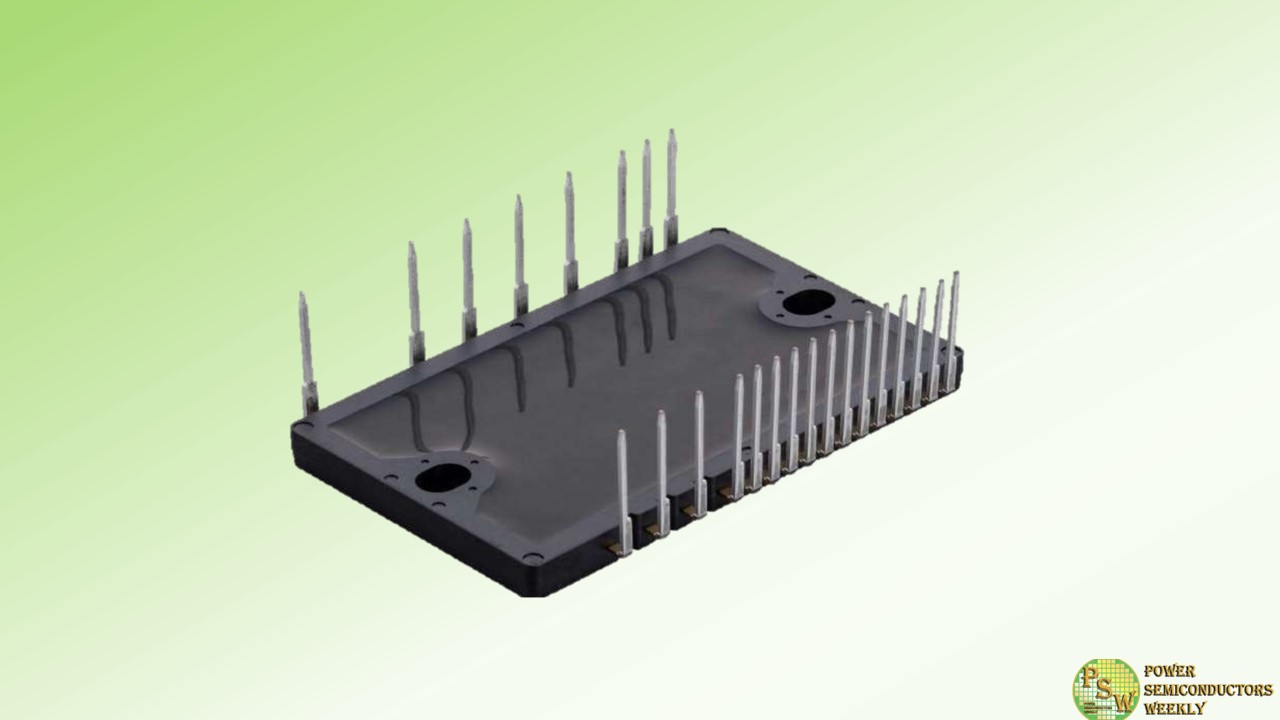
Fuji Electric Co., Ltd. announced the launch of the P633C Series 3rd-generation small IPMs, which help reduce the power consumption of the equipment on which it is mounted, such as home appliances and machine tools.
IPMs (intelligent power modules) are power semiconductors equipped with a built-in IGBT drive circuit and protection function. They are used for applications including inverters and servo systems. Inverters and servo systems control machine operation by controlling voltage and frequency through power semiconductor switching (turning electricity on and off), but power semiconductors generate power loss and electromagnetic noise during switching.
This product can reduce both the power loss and the electromagnetic noise generated during switching. Using this product in inverters for home appliances or servo systems for machine tools can reduce the power consumption of the equipment on which it is mounted, thereby contributing to the achievement of a decarbonized society.
One way to reduce the power loss that occurs during switching is to speed up the switching operation. Faster switching increases electromagnetic noise, which can cause peripheral devices to malfunction. This product uses the latest 7th-generation IGBT/FWD chips, achieving a 10% reduction of power loss and a reduction of electromagnetic noise to approximately 1/3 compared with conventional products. The trade-off characteristics between power loss and noise are among the best in the industry.
Original – Fuji Electric
-
Semiconductor industry players Robert Bosch GmbH, Infineon Technologies AG, Nordic Semiconductor, NXP® Semiconductors, and Qualcomm Technologies, Inc., have come together to jointly invest in a company aimed at advancing the adoption of RISC-V globally by enabling next-generation hardware development.
Formed in Germany, this company will aim to accelerate the commercialization of future products based on the open-source RISC-V architecture. The company will be a single source to enable compatible RISC-V based products, provide reference architectures, and help establish solutions widely used in the industry. Initial application focus will be automotive, but with an eventual expansion to include mobile and IoT.
At its core, RISC-V encourages innovation, allowing any company to develop cutting-edge, customized hardware based on an open-source instruction set. Further adoption of the RISC-V technology will promote even more diversity in the electronics industry – reducing the barriers to entry for smaller and emergent companies and enabling increased scalability for established companies.
The company calls on industry associations, leaders, and governments, to join forces in support of this initiative which will help increase the resilience of the broader semiconductor ecosystem.
The company formation will be subject to regulatory approvals in various jurisdictions.
- Robert Bosch GmbH
“Bosch is convinced that initiatives promoting the RISC-V open specifications will bring the global mobility market a significant step further. The initiative now planned will greatly help to establish a reliable and efficient EU-based semiconductor ecosystem,” said Jens Fabrowsky, Executive Vice President at Bosch and responsible for the semiconductor business.
- Infineon Technologies AG
“As vehicles become software-defined and dependability requirements increase due to electrification and connectivity, for example, as well as through trends like autonomous driving, there is a general need for standardization and ecosystem compatibility across the industry, with CPUs being a key IP. We are proud to support the establishment of trusted RISC-V based automotive products with this initiative. The knowledge and expertise of leading market players will unleash the full potential of RISC-V in the automotive sector,” said Peter Schiefer, Division President of Infineon’s Automotive Division.
- Nordic Semiconductor
“Nordic Semiconductor is a committed and enthusiastic supporter of the RISC-V initiative and stands ready to drive the project forward. Nordic’s IoT solutions represent the leading edge of low power wireless technology and to retain that position it’s critical we maintain continuous access to efficient and powerful embedded microprocessors. An open collaboration with like-minded companies to continually enhance innovative RISC-V microprocessor IP and ensure a robust and reliable supply of the technology is the ideal answer to this challenge,” said Svein-Egil Nielsen, CTO/EVP R&D and Strategy, Nordic Semiconductor.
- NXP Semiconductors
“NXP is proud to be part of a new EU-based joint endeavor to pioneer fully certified RISC-V-based IP and architectures, initially for the automotive industry. The creation of a one-stop-shop ecosystem where customers can select turnkey assets will strengthen the adoption of RISC-V across many European industries,” said Lars Reger, Executive Vice President and Chief Technology Officer at NXP Semiconductors. “We thank the Artificial Intelligence Center Hamburg (ARIC) e.V. for their support of this collaboration.”
- Qualcomm Technologies, Inc.
“We are excited to come together with other industry players to drive the expansion of the RISC-V ecosystem through development of next-generation hardware. Qualcomm Technologies has been investing in RISC-V for more than five years and we’ve integrated RISC-V micro-controllers into many of our commercial platforms. We believe RISC-V’s open-source instruction set will increase innovation and has the potential to transform the industry,” Ziad Asghar, Senior Vice President of Product Management, Qualcomm Technologies, Inc.
Original – Infineon Technologies
-

Navitas Semiconductor announced that its CRPS185 3,200 W “Titanium Plus” server reference design not only surpasses the stringent 80Plus Titanium efficiency requirements, but also effectively satisfies the increasing power demands of AI data center power.
The rapid development and deployment of artificial intelligence (AI) including OpenAI’s ChatGPT, Microsoft’s Bing with AI, and Google’s Bard, has penetrated all aspects of people’s lives. New power-hungry AI processors like NVIDIA’s DGX GH200 ‘Grace Hopper’ demand up to 1,600 W each, are driving power-per-rack specifications from 30-40 kW up to 100 kW per cabinet. Meanwhile, with the global focus on energy conservation and emission reduction, as well as the latest European regulations, server power supplies must exceed the 80Plus ‘Titanium’ efficiency specification.
Navitas’ reference designs dramatically accelerate customer developments, minimize time-to-market, and set new industry benchmarks in energy efficiency, power density and system cost, enabled by GaNFast power ICs. These system platforms include complete design collateral with fully-tested hardware, embedded software, schematics, bill-of-materials, layout, simulation and hardware test results.
In this case, the ‘Common Redundant Power Supply’ (CRPS) form-factor specification was defined by the hyperscale Open Compute Project, including Facebook, Intel, Google, Microsoft, and Dell. Now, Navitas’ CRPS185 platform delivers a full 3,200 W of power in only 1U (40 mm) x 73.5mm x 185 mm (544 cc), achieving 5.9 W/cc, or almost 100 W/in3 power density. This is a 40% size reduction vs, the equivalent legacy silicon approach and easily exceeds the Titanium efficiency standard, reaching over 96.5% at 30% load, and over 96% stretching from 20% to 60% load, creating a ‘Titanium Plus’ benchmark, critical for data center operating models.
The CRPS185 uses the latest circuit designs including an interleaved CCM totem-pole PFC with full-bridge LLC. The critical components are Navitas’ new 650V GaNFast power ICs, with robust, high-speed integrated GaN drive to address the sensitivity and fragility issues associated with discrete GaN chips. Additionally, GaNFast power ICs offer extremely low switching losses, with a transient-voltage capability up to 800 V, and other high-speed advantages such as low gate charge (Qg), output capacitance (COSS) and no reverse-recovery loss (Qrr). As high-speed switching reduces the size, weight and cost of passive components in a power supply, Navitas estimates that GaNFast power ICs save 5% of the LLC-stage system material cost, plus $64 per power supply in electricity over 3 years.
Compared to traditional ‘Titanium’ solutions, the Navitas CRPS185 3,200 W ‘Titanium Plus’ design running at a typical 30% load can reduce electricity consumption by 757 kWh, and decrease carbon dioxide emissions by 755 kg over 3 years. This reduction is equivalent to saving 303 kg of coal. Not only does it help data center clients achieve cost savings and efficiency improvements, but it also contributes to the environmental goals of energy conservation and emission reduction.
In addition to data center servers, this solution can also be widely used in applications such as switch/router power supplies, communications, and other computing applications.
“The popularity of AI applications like ChatGPT is just the beginning. As data center rack power increases by 2x-3x, up to 100 kW, delivering more power in a smaller space is key,” said Charles Zha, VP and GM of Navitas China. “We invite power designers and system architects to partner with Navitas and discover how a complete roadmap of high efficiency, high power density designs can cost-effectively, and sustainably accelerate their AI server upgrades.”
Original – Navitas Semiconductor
