-
During the past decade combination “silicon carbide” or more often “SiC” has become very popular in the world of power electronics. Many companies have started to evaluate the possibility of using SiC instead of Si in their projects. As many say, silicon carbide is here to replace silicon, and they might be right considering that SiC MOSFETs used in power semiconductor devices bring numerous advantages compared with their silicon counterparts.
SiC has a higher critical breakdown field and thermal conductivity and, a wider bandgap, which leads to lower energy losses, a lower leakage current at higher temperatures. Besides, SiC can operate at much higher frequencies. On a system level, it means using less additional components, better thermal management, and an overall smaller footprint.
This is one of the reasons why today automotive Tier-1 and OEM companies prefer to use SiC for their new projects in vehicle electrification. With SiC they can get the same efficiency with several times smaller package. For the electric car size and weight of power electronics systems are critical.
Working in the power semiconductors industry for many years, with Si and SiC power devices in particular, I see that the number of companies and end applications adopting silicon carbide is growing fast. Even though SiC is quite a young technology, and the first commercial SiC power MOSFET dates back to 2011, nowadays, we already have over ten SiC power device vendors who deliver high-quality products used in electric vehicles, solar inverters, public transportation, welding equipment, marine, medical and aerospace.
With the number of new SiC fabs and production expansions announced during the past three years it is clear that silicon carbide technology is here to stay, and here to grow further. Many analytical agencies predict that the total SiC market will reach 10 billion USD by 2030 or even earlier. And despite the fact that in volume SiC power semiconductors market still lags behind silicon. It grows faster, quite faster than expected several years ago.
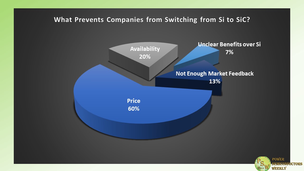
Despite the fast growth and penetration into the power electronics market, many companies still feel uncomfortable when they hear about silicon carbide and the benefits it has. During numerous negotiations and talks with the companies using power semiconductor devices, I shortlisted the most common barriers preventing them from switching from silicon to silicon carbide, or from increasing the number of SiC-based projects they already have.
To further scale this data, recently I had a poll on LinkedIn within the power electronics community. A similar poll I ran during the latest EPE’23 ECCE Europe Conference, which was held in Aalborg, Denmark. Both polls’ participants come from power semiconductors companies or from companies using power semiconductors.
Combined poll results look like this:
- Price – 60%
- Availability – 20%
- Unclear benefits over Si – 7%
- Not enough market feedback – 13%
It is clear that price is still the major concern and barrier. Even though the price has tremendously decreased during the past ten years, it remains one of the key factors why many companies prefer to use Si-based semiconductors.
The availability of SiC wafers or SiC-based devices accounts for another 20% of doubts coming from the end users. The lead time of SiC has been discussed many times, and the situation for many stays unclear. And it is the same for the remaining 20% of poll results coming from unclear benefits of SiC and lack of market feedback. Silicon power devices have been in use for decades, while SiC is just at the beginning of its road. That is why many engineers prefer to work with the technology they know, the technology they have been very familiar with since their school.
From the first look the answers and results of the poll seem to be right and they correspond to the current market situation. However, working with Si and SiC, I know that each and every one of the answers listed are just the barriers and not the final verdict.
Semiconductor companies should pay more attention to those 20% of the answers referring to lack of market data. With the right approach SiC will bring the power semiconductors industry to a new level.
-
Navitas Semiconductor announced the 2023 Investor Day, to be held at the company’s new headquarters, on Tuesday 12th December, 2023.
Meeting highlights include:
- Four major new GaN/SiC technology platforms and five focus markets, including new GaNSafe technology, positioned to revolutionize AI-based data centers, EV, and renewable applications.
- Invited customer presentations, with leading-edge applications enabled by Navitas.
- $1B+ customer pipeline & what this means to Navitas growth trajectory, with a preview of 2024 forecast and long-term targets.
- Navitas’ unique, detailed view on the past, present and future of power electronics as we look to “Electrify Our World” (guided tour, and management small-group meetings).
For in-person attendance or participation virtually via live-stream, please contact ir@navitassemi.com
Original – Navitas Semiconductor
-
Infineon Technologies AG has taken over as head and coordinator of the broad-scope European research project EECONE (European ECOsystem for greeN Electronics), intended to make electronics in Europe more sustainable. The objective is to investigate the corresponding technologies along the entire value chain, from design, manufacture and use all the way to recycling. EECONE is one of the Key Digital Technologies research projects supported by the European Union as a Joint Undertaking. 49 partners are participating in the project, which has a volume of approximately 35 million euros total costs. The project is being funded by the European Union and the national governments of the participating companies with around 20 million euros.
“Electronics are fundamental to improving the sustainability of many applications. But this is not sufficient, electronics themselves have to become greener,” says Constanze Hufenbecher, Infineon Management Board member and Chief Digital Transformation Officer. “Infineon is pleased to take on the lead role in the research project EECONE in order to advance the circular economy together with our partners along the value chain. The only way to achieve sustainability from design and use and all the way to recycling is by working together.”
EECONE is aligned with the 6R concept (Reduce, Reliability, Repair, Reuse, Refurbish, Recycle); the amount of materials required by electronics is to be reduced, electronics are to be made more reliable, easier to fix and use again, and easier to recondition and to recycle. The project will investigate a total of ten application examples from the widest possible variety of fields in terms of developing green electronics. The applications are from the areas Automotive, Consumer Electronics, Health, Information and Communication Technologies, Aviation and Agriculture.
Focus points are for example reducing the amount of material used by making circuit boards thinner or smaller, or improving sustainability by introducing materials which are easier to separate during recycling. Facilitating the replacement of not only circuit boards but also of semiconductors is to make it easier to repair devices. The technologies involved could also make it possible to reuse and recycle electronic components. The project will in addition develop technologies which for example generate and store their own power in IoT devices.
New, ecologically friendly materials are to make it easier to recycle lithium-ion batteries. Artificial Intelligence will be used to prolong the service lives of electronic equipment, while tools for more sustainable electronic design, including comprehensive impact assessments for the use of electronics, are to be developed as well. EECONE also covers the use, dissemination and standardization of electronics and will train specialists in handling electronic refuse.
The EECONE research project has a planned duration of three years. It will establish decisive foundations for the sustainable development, manufacturing and use of electronics in Europe. The on-site inaugural event of the project will be held in Toulouse on 20 and 21 September 2023.
The 49 EECONE Research Project Partners
- 4Mod Technology (FR)
- Acorde Technologies Sag (ES)
- Agencia Estatal Consejo superior de Investigaciones cientificas (ES)
- Aniah SAS (FR)
- Arcelik A.S. (TR)
- Atea Sverige AG (SE)
- AT&S – Austria Technologie & Systemtechnik (AT)
- Centre national de la Recherche scientifique (FR)
- Charokopeio Panepstimio (EL)
- Commissariat a l’Energie atomique et aux Energies alternatives (FR)
- Dassault Systemes (FR)
- Design and Reuse (FR)
- EcoDC AG (SE)
- Fraunhofer Gesellschaft zur Forderung der angewandten Forschung e.V. (DE)
- Get electronique (FR)
- Infineon Technologies AG (DE)
- Institut mikroelektronickych Aplikaci SRO (CZ)
- Institut polytechnique de Grenoble (FR)
- Interactive fully electrical Vehicles SRL (IT)
- Interuniversitair Microelectronica Centrum (BE)
- Leonardo – Societa per Azioni (IT)
- Luna Geber Engineering SRL (IT)
- Melsen Tech A/S (DK)
- Nerosubianco SRL (IT)
- Orbotech Ltd. (IL)
- Ozyegin Universitesi (TR)
- Premo, S.L. (ES)
- Research Institutes of Sweden AB (SE)
- Robert Bosch GmbH (DE)
- Siec Badawcza Lukasiewecz – Instytut Mikroelektronik i Fotoniki (PL)
- Silicon Austria Labs GmbH (AT)
- Smartsol SIA (LV)
- Soitec SA (FR)
- STMicroelectronics SAS (FR)
- Synano BV (NL)
- Technicka Univerzita v Liberci (CZ)
- Technische Hochschule Deggendorf (DE)
- Tecnologias Servicios telematicos y Sistemas SA (ES)
- Teknologisk Institut (DK)
- Tetradis (FR)
- Thales dis France SAS (FR)
- Università degli Studi di Perugia (IT)
- Université catholique de Louvain (BE)
- Université Grenoble Alpes (FR)
- Ustav teorie informace a Automatzizace AV CR VVI (CZ)
- Vitesco Technologies France (FR)
- Weeecycling (FR)
Associated Partners
- Centre Suisse d’Electronique et de Microtechnique SA – Recherche et Developpement (CH)
- Swiss Vault Systems GmbH (CH)
Original – Infineon Technologies
-

The U.S. Department of Defense (DoD) has awarded GlobalFoundries (GF) a new 10-year contract for a supply of securely manufactured, U.S.-made semiconductors for use across a wide range of critical aerospace and defense applications.
With an initial award of $17.3 million this month and an overall 10-year spending ceiling of $3.1 billion, the new contract provides the DoD and its contractors with access to GF’s semiconductor technologies manufactured at its U.S. facilities. These GF facilities are DoD-accredited to the highest security level, Trusted Supplier Category 1A, which implements proven stringent security measures to protect sensitive information and manufacture chips with the highest levels of integrity to ensure they are uncompromised.
In addition to secure chip manufacturing for DoD systems used on land, air, sea, and in space, the new contract provides the DoD and its contractors with access to GF’s robust design ecosystem, IP libraries, early-access to new technologies in development, quick and efficient prototyping, and full-scale volume manufacturing. The contract was awarded through the DoD’s Defense Microelectronics Activity (DMEA) Trusted Access Program Office (TAPO).
“GF is proud to begin this new chapter of our decades-long partnership with the U.S government, and to continue serving as the leading supplier of securely manufactured essential chips for the U.S. aerospace and defense industry,” said Mike Cadigan, chief corporate and government affairs officer at GF. “This partnership provides DoD programs with ‘front-door access’ to advanced technologies in a way that is scalable and highly efficient. For this work, GF is accredited to provide the right level of security required for each program, from GF’s industry leading GF Shield protections, to strictly export controlled handling (e.g. ITAR), to the highest level of accredited microelectronics manufacturing security on the planet, Trusted Category 1A.”
This new contract is the third sequential 10-year contract of its kind between the DoD and the Trusted Foundry business team at GF and is the latest milestone in the longstanding partnership between the department and the company.
Original – GlobalFoundries
-

NXP Semiconductors N.V. has been honored by three automotive partners. The company has collected supplier awards from DENSO and Hyundai Motor Group for its outstanding efforts in helping to ensure supply capacity, continuity and excellent customer service, as well as an innovation award from BMW Group for its digital car key solution.
“Successfully navigating the auto industry’s complex supply chain landscape to deliver true innovation our customers need can only be achieved through close collaboration with semiconductor manufacturers, Tier 1s and OEMs. We are extremely proud to be honored by BMW Group for our innovative UWB based digital car key solution, and by both DENSO and Hyundai Motor Group for NXP’s steadfast commitment to meeting our customer’s needs. Our teams work tirelessly to develop breakthrough technologies and foster collaborative customer relationships that enable NXP to deliver strategic long-term forecasts and expand capacity where needed, despite challenging conditions.”
Ron Martino, Executive Vice President, Global Sales at NXP
DENSO’s Business Partner of the Year Awards are given to companies that demonstrate a shared commitment to outstanding performance, exceptional quality, sustainability, diversity and inclusion, and advancing mobility. DENSO’s Gold Award for Special Achievements recognizes NXP’s outstanding efforts to ensure business continuity despite difficult supply conditions while maintaining strong customer service levels.
“This past year has been defined by an urgent need to adapt and evolve for emerging mobility trends, from electrification to connectivity and much more. All of our partners, but especially award recipients, have been crucial in helping us navigate such changes and deliver for our customers – quickly, sustainably and with enhanced value.”
Mike Winkler, vice president of the North America Purchasing Group at DENSO
In April, NXP received the prestigious 2022 Global Supplier of the Year award from Hyundai Motor Group, making NXP one of the first semiconductor vendors to receive such recognition. The award highlights the significance of the strong collaboration between semiconductor suppliers and auto OEMs from a supply and supply assurance viewpoint. It also recognizes NXP’s outstanding local team support and engagement in Korea.
In collaboration with Continental Automotive GmbH Regensburg, NXP was also awarded the BMW Group Supplier Innovation Award for the company’s innovative digital car key solution that leverages Ultra-Wideband technology. The digital key enables drivers to unlock their cars securely with their smartphones without needing a physical car key.
Original – NXP Semiconductors
-
CDIL Semiconductors (Continental Device India Pvt. Ltd.), India’s first semiconductor chips and components manufacturer, will be adding new semiconductor packaging lines via the Government of India and MeitY’s SPECS scheme. With the new lines, CDIL aims to increase its annual capacity by 100 million units. The company initiated the first phase of this production with a surface mount packaging line of 50 million devices that will be inaugurated on September 28th, 2023 by Shri Rajeev Chandrasekhar Ji, Hon’ble Union Minister of State for Electronics and Information Technology & Skill Development and Entrepreneurship.
With 59 years of legacy, CDIL today is a semiconductor and electronics service provider to a worldwide customer base across Consumer, Industrial, Defence, Aerospace and Automotive. The company has many industry leaders as long term customers spread throughout the world including USA, UK, Germany, China, Hong Kong, Japan, South Korea, South Africa, and Egypt.
Commenting on the expansion of the product lines, Prithvideep Singh, General Manager, CDIL Semiconductors said, “In line with our steadfast commitment to innovation and market diversification, CDIL Semiconductors has strategically positioned itself to meet the burgeoning demands of the industry especially the power electronics, automotive, and defence sectors, both within India and on a global scale. As we reflect upon this progress, we recognize that this is only the beginning. The groundwork has been established and will stand as a pivotal cornerstone for the company’s future endeavours.”
CDIL has established an advanced high reliability (HiRel) and testing laboratory located at Mohali in addition to its NABL Accredited facility in Delhi. The HiRel laboratory is a crucial part of qualifying CDIL’s devices for stringent sectors like Automotive, Defence, and Aerospace.
Being the 1st Indian semiconductor company to obtain the IS/ISO 9002 and IATF 16949 quality system certifications, CDIL was the first to introduce India to silicon semiconductor technology in 1964. Currently, it produces a comprehensive range of discrete semiconductor devices including Transistors, Diodes, Rectifiers, Schottky Diodes, Thyristors, Voltage Regulators, Transient Voltage Suppressors and MOSFETS, with specialities in power Semiconductors, and high-reliability components.
Original – CDIL Semiconductors
-
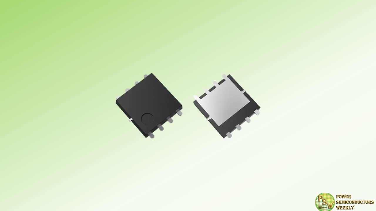
Toshiba Electronic Devices & Storage Corporation has started mass production of three 40 V N-channel MOSFETs using SOP Advance(WF) package for automotive and has expanded its lineup. The three models are “XPHR9904PS, XPH2R404PS and XPH3R304PS.”
The new products reduce drain-source On-resistance with the U-MOSIX process as with Toshiba’s precedence release products XPHR7904PS and XPH1R104PS. The drain-source On-resistance of XPH2R404PS is 2.4 mΩ (max), which is approximately 27 % lower than that of Toshiba’s existing product TPCA8083, and XPH3R304PS is 3.3 mΩ (max), which is approximately 42 % lower than that of Toshiba’s existing product TPCA8085.
The drain-source On-resistance of XPHR9904PS is 0.99 mΩ (max). Reducing drain-source On-resistance of these products contributes to low power consumption of automotive equipment. In addition, they are qualified with the automotive reliability standard AEC-Q101. The PPAP of IATF16949 is also available.
The package is a surface mount type SOP Advance(WF) that uses a wettable flank terminal structure, which facilitates automated visual inspection of the board mounting state.
Toshiba’s automotive MOSFETs support a variety of automotive applications and meet a wide range of customer needs.
Applications
- Automotive equipment: motor drives, switching power supplies, load switches, etc.
Features
- Low On-resistance
XPHR9904PS: RDS(ON)=0.99 mΩ (max) (VGS=10 V)
XPH2R404PS: RDS(ON)=2.4 mΩ (max) (VGS=10 V)
XPH3R304PS: RDS(ON)=3.3 mΩ (max) (VGS=10 V) - AEC-Q101 qualified
- PPAP of IATF16949 available
Original – Toshiba
-
Power semiconductors based on silicon carbide (SiC) offer several advantages, like high efficiency, power density, voltage resistance, and reliability. This creates opportunities for new applications and improved charging station technology innovations. Infineon Technologies announced a collaboration with Infypower, a Chinese market leader in new energy vehicle charging. Infineon will provide INFY with the industry-leading 1200 V CoolSiC™ MOSFET power semiconductor devices to improve the efficiency of electric vehicle charging stations.
“The collaboration between Infineon and Infypower in the field of charging solutions for electric vehicles (EV) provides an excellent system-level technology solution for the local EV charging station industry,” said Dr. Peter Wawer, Division President of Infineon’s Green Industrial Power Division. “It will significantly improve charging efficiency, accelerate charging speed, and create a better user experience for owners of electric cars.”
“With Infineon’s more than 20 years of continuous advancement in SiC product offering and the strength of integrated technology, Infypower can consolidate and maintain its technological outstanding position in the industry by adopting state-of-the-art product processes and design solutions“, said Qiu Tianquan, President of Infypower China. “We can also set a new standard for charging efficiency of DC chargers for new energy vehicles. As a result, customers can enjoy more convenience and unique value, promoting the healthy development of the EV charging industry.”
SiC’s high power density enables the development of high-performance, lightweight, and compact chargers, especially for supercharging stations and ultra-compact wall-mounted DC charging stations. Compared to traditional silicon-based solutions, SiC technology in EV charging stations can increase efficiency by 1 percent, reducing energy losses and operating costs. In a 100 kW charging station, this translates to 1 kWh of electricity savings, saving 270 Euros annually and reducing carbon emissions by 3.5 tons. This drives the increasing adoption of SiC power devices in EV charging modules.
As one of the first SiC power semiconductor manufacturers to use trench gate technology for transistors, Infineon has introduced an advanced design that provides high reliability for chargers. The devices offer a high threshold voltage and simplified gate driving . The CoolSiC MOSFET technology has been subjected to marathon stress tests and gate voltage jump stress tests before commercial release and regularly afterwards in form of monitoring to ensure highest gate reliability.
By integrating Infineon’s 1200 V CoolSiC MOSFETs, Infypower’s 30 kW DC charging module offers a wide constant power range, high power density, minimal electromagnetic radiation and interference, high protection performance and high reliability. In this way, it is well suited for the fast charging demand of most EVs while possessing a higher efficiency of 1 percent compared with other solutions on the market. Consequently, significant energy savings and carbon dioxide emission reduction are achieved, which are leading at a global level.
Original – Infineon Technologies
-
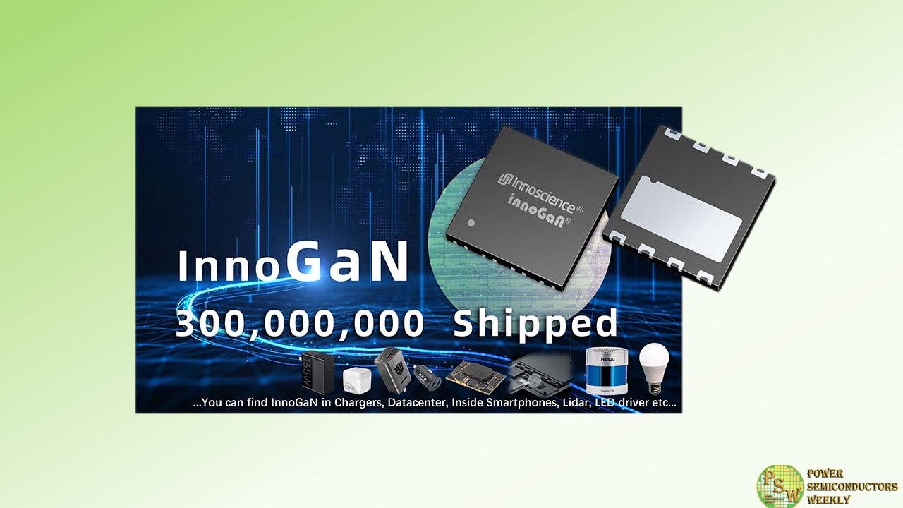
Innoscience Technology has shipped more than 300 million pieces of its InnoGan gallium nitride chips as of August 2023, helping customers achieve small size, high energy efficiency, and low loss product design.
This is in response to phenomenal market demand across multiple sectors multiple applications in the consumer category – fast charging, mobile phones, LEDs – as well as automotive LIDAR, data centres, and renewable energy and energy storage systems, which has seen analysts such as TrendForce’s in its 2023 GaN Power Semiconductor Market Analysis Report, state that “the global GaN power device market will grow from US$180 million in 2022 to US$1.33 billion in 2026, with compound growth rate of 65%”.
In November 2017, Innoscience began the world’s first 8-inch GaN-on-Si mass production line, adopting the Integrated Device Manufacturer (IDM) whole industry chain model, and launched its first low-voltage GaN power device in May 2018. By June 2019, Innoscience’s 650V high-voltage GaN device had passed JEDEC approval, and subsequently, Innoscience has been the only semiconductor company in the world that simultaneously mass-produces high-voltage and low-voltage GaN.
Market acceptance of Innoscience’s high quality, high performance GaN devices has been swift. Following its 2019 entry into the fast charging market, Innoscience’s 650V parts have been adopted in 30W-120W designs by leading brands including ASUS, Anker, Nubia, Baseus, Greenlink, and Flash.
In 2020, Innoscience’s 100V low-voltage GaN was successfully used by Hesai in mass-production LIDAR designs, allowing lasers to achieve image transmission in a shorter time.
In March 2021, the Tencent×Nubia Red Magic mobile phone 6Pro was released. It comes equipped as standard with industry’s first 120W Black Rubik’s Cube GaN fast charge, which is based on Innoscience’s 650V chip. With the successive adoption by Oppo, Vivo, Lenovo and other manufacturers, it has become an industry trend for mobile phones to be equipped with GaN fast charging as standard.
March 2021 saw the mass-production of Innoscience’s bi-directional conduction chip V-GaN officially begin; this device is the only GaN chip in the world that can be applied to high-voltage side load switches, smartphone USB/wireless charging ports with built-in OVP protection, multi-power supply system switch circuits, and other scenarios:one V-GaN replaces two Si MOSFETs in load switching applications resulting in a smaller and more efficient solution.
In October of the same year, Innoscience scored another industry first, as OPPO used the company’s self-developed bi-directional conduction VGaN IC as the internal power switch in its latest smart phone. Other mobile phone makers such as Realme, OnePlus, Lenovo, and Motorola have also successively adopted VGaN for charging protection.
In May 2022, Shounuo released the world’s smallest 45W/65W PD car charger, using Innoscience’s 40V low-voltage INN040FQ043A.
Then in July, Anker and Innoscience jointly released the world’s first 65W full-GaN fast charger. This design uses GaN power chips at both the AC and DC ends for the first time, taking system power density and efficiency to a whole new level.
Later, in October 2022, Innoscience achieved mass production of GaN products targeting industrial power supplies – again an industry first – comprehensively improving energy conversion efficiency and reducing system energy consumption.
In November 2022, Innoscience’s INN100W032A won the IIC World Electronics Achievement Award. The gate charge of this product is only 20% of a traditional silicon MOSFET, and its Ciss is only 40% of its silicon counterpart. It can be widely applied in motor drive, Class D, data centre, motor-driver, communication base station and other product fields. In January 2023, Innoscience launched the SolidGaN ISG3201, a 100V highly-integrated half-bridge drive packaged solution, further improving the overall system performance of 48V power supply of data centre module power supplies, motor drives, class D power amplifiers, photovoltaic inverters and light hybrid electric vehicles.
The move to GaN as the premium power semiconductor technology is driven both by new GaN products and market demands. As an example, in April this year, Innoscience’s IATF 16949 automotive-grade low-voltage parts successfully expanded from industrial to automotive applications, with use in autonomous vehicle LIDAR systems.
Then in July 2023, Innoscience began to apply GaN in the field of renewable energy, reducing the size and improving the efficiency of photovoltaic modules.
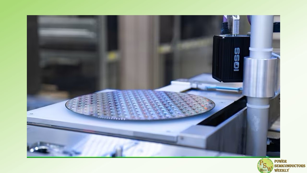
By the end of August 2023, Innoscience had successfully mass-produced 54 different types of high-voltage GaN chips (650V-700V) and 20 types of medium-low voltage GaN chips (30V-150V). Products span three chip categories: wafers, discrete devices and integrated solutions.
Commented Dr Denis Marcon, Innoscience’s General Manager, Europe: “We are just at the start of the GaN story. The first applications were all in consumer, but GaN is undoubtedly the key to reducing costs and increasing efficiency in the industrial field as well. And according to automotive industry forecasts, GaN may enter automotive market already this year penetrating applications such as low-power OBC and DC-DC applications in 2025.
With such rapid growth in market demand, the reliability of devices, price competitiveness and stable supply in large quantities are now the major concerns of users. Based on an advanced Innoscience’s 8-inch GaN-on-Si IDM manufacturing platform, Innoscience’s current production capacity has reached 15,000 wafers per month, providing tremendous advantages in scale, reliability and cost.”
Original – Innoscience Technology
-
NXP Semiconductors N.V. announced it is strengthening its European research and development (R&D) through grants to be provided via the 2nd Important Project of Common European Interest on Microelectronics and Communication Technologies (IPCEI ME/CT), with the final investment decision pending confirmation of the level of public funding. Dedicated NXP teams across Austria, Germany, the Netherlands and Romania will innovate in core technologies across automotive, industrial and cybersecurity. This includes 5nm, advanced driving assistance and battery management systems in automotive, 6G and Ultra-Wideband as well as artificial intelligence (AI), RISC-V and post-quantum cryptography.
“NXP’s planned investments in our Austrian, German, Dutch, and Romanian operations signal our strong commitment to the EU’s goal of enabling both digital and green transition. Our activities through IPCEI ME/CT complement NXP’s planned joint venture participation in TSMC’s first European foundry. It also underscores our commitment to strengthening innovation and supply chain resilience in Europe. NXP believes expanding research, development, and manufacturing efforts in Europe is of vital importance, and each of these three critical elements must be successfully integrated to achieve greater European semiconductor ecosystem resilience.”
Kurt Sievers, President and CEO of NXP
Extensive research, development, and manufacturing presence across multiple sites in all four countries enable NXP to develop cutting-edge technology and products that contribute significantly to the achievement of EU industrial strategies. In close collaboration with a strong ecosystem of more than 50 partners from industry and academia across Europe, NXP will strengthen key technologies of microelectronics in Europe.
No other microelectronics company participating in IPCEI ME/CT is currently planning to invest in its operations across so many EU member states. NXP is also an active participant in three of the four IPCEI ME/CT workstreams: “Sense”, “Think”, and “Communicate”, reflecting NXP’s areas of leadership and strategic focus.
NXP’s planned investments in Austria, Germany, the Netherlands, and Romania follow the announcement that the company is going to form a new joint venture, ESMC (European Semiconductor Manufacturing Company), with TSMC, Bosch, and Infineon with plans to establish TSMC’s first semiconductor manufacturing site in Europe. The new 300mm fab, planned to be built in Dresden, Germany, is expected to have a monthly production capacity of 40,000 300mm (12-inch) wafers on TSMC’s 28/22 nanometer planar CMOS and 16/12 nanometer FinFET process technology, further strengthening Europe’s semiconductor manufacturing ecosystem with advanced FinFET transistor technology and creating about 2,000 direct high-tech professional jobs.
NXP in Austria
NXP Austria is a center of excellence for cryptography and security, advancing solutions that make lives easier, better and safer. NXP Austria innovates hardware and software solutions as well as services for the IoT, automotive, Industry 4.0 and mobile sectors. At NXP Austria, nearly 800 people from approximately 50 countries work on Innovations to research, design, develop, manage, and promote NXP’s products.
For more information on NXP in Austria, visit nxp.com/austria
NXP in Germany
With over 1,200 people, Germany is a very important R&D hub for NXP with a focus on semiconductor solutions for the automotive market as well as secure connected edge applications, such as industrial IoT, mobile, and wearables. Primary R&D competencies in Hamburg, Munich, and Dresden include cybersecurity, automotive processing, and RF. A collaborative quantum computing initiative was established in 2023 in Hamburg. IPCEI will help to further strengthen and expand these core competencies. In addition, the German sites are home to an experienced sales engineering team that completes NXP’s global network of customer support.
For more information on NXP in Germany, visit nxp.com/germany
NXP in the Netherlands
NXP has over 2,200 people and significant operations across three sites in the Netherlands. NXP’s international headquarters is located on the High Tech Campus Eindhoven. R&D groups based in Eindhoven focus on security innovation, software and hardware IP development, chip design, system innovation and certification. NXP Nijmegen features manufacturing, R&D, testing, technology enablement and support functions. NXP’s Delft site is home to hardware and software design teams focusing on secure wireless solutions including automotive electronics such as radio, GPS, car access systems, and sensor electronics.
For more information on NXP in the Netherlands, visit nxp.com/netherlands
NXP in Romania
NXP Bucharest’s over 1,000 people focus on software development for automotive, microcontrollers and connectivity products as well as IT service management and customer supply operations. Each year, NXP Romania hosts interns who learn the specifics of software development in automotive, edge computing and IoT.
For more information on NXP in Romania, visit nxp.com/romania
Original – NXP Semiconductors
