-
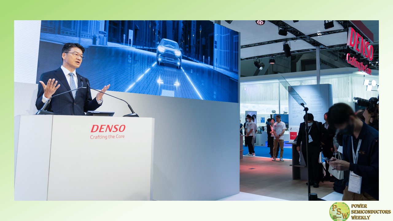
DENSO CORPORATION hosted a press conference at JAPAN MOBILITY SHOW 2023 held at Tokyo Big Sight on October 26. Shinnosuke Hayashi, President and COO introduced the strategy to maximize company’s contributions to “Green” and “Peace of Mind.”
Shinnnouke Hayashi, President and COO of DENSO CORPORATION said that it is a great pleasure that the Tokyo Motor Show, which has attracted much public attention for decades, has been renamed the JAPAN MOBILITY SHOW. This change reflects the fact that we are entering an era of creating new value by addressing various issues from the viewpoint of a mobility-centered society instead of just vehicles and by connecting people and technologies across industries. This means that DENSO must meet major challenges.
To evolve from “a Tier 1 supplier that supports the auto industry “to “a Tier 1 supplier that supports a mobility-centered society” to create value for more diverse customers, the company addresses three intiatives. To promote these three initiatives, DENSO will recruit new employees in the electrification and software field and actively shift the employees from the mature field to the electrification and software fields and strengthen about 4,000 employees during the four years from 2022 to 2025.- The contribution to the “evolution of mobility”
In the “Green” field, “the environment”, in addition to the product lineup in the “horizontal” direction to enable installation in HEVs, PHEVs, BEVs, and FCEVs, the lineup will be expanded in the “vertical” direction ranging from large systems, which link electrification products with energy management, to components, including power modules, thereby meeting the needs of various customers as BEVs proliferate and helping to achieve carbon neutrality in respective countries. In the “Peace of Mind” field, “worry-free society”, in addition to around-vehicle monitoring systems, DENSO will focus on driver status monitoring systems and cloud-based large systems, which connect with the social infrastructure. Through these efforts, the company will help eliminate fatalities.
Furthermore, DENSO will extend its commitment to the evolution of mobility to the sky to help realize more freedom of traveling and expand the possibilities of mobility.
- The challenge to “to create new value”
DENSO has been studying the possibility of developing and commercializing many technologies in non-mobility fields, including energy, food and agriculture, and the circular economy. Specifically, the company plans to market energy system products such as Solid Oxide Electrolysis Cell and Solid Oxide Fuel Cell in 2024 and beyond.
- Strengthening semiconductors and software
In terms of semiconductors, DENSO will actively invest about 500 billion yen by 2030. DENSO will triple the scale of the business from the current level by 2035. To expand production, the company must ensure stable procurement of materials. Thus, DENSO will forge strategic partnerships with various companies.
In the softaware field, the implementation phase to embody concepts, the company will accelerate the planning of electronic platform and over-the-air technology development based on user needs while strengthening partnerships with various customers and promote integrated development across companies. DENSO will increase the number of software engineers and improve their skills and integrate two group companies which have excellent proprietary technologies, into DENSO. One is NSITEXE, which specializes in the semiconductor intellectual property, and the other is AUBASS, which specializes in developing basic in-vehicle software. DENSO will double the speed of development by applying specialized AI, which incorporates company’s knowledge and experience gained through in-vehicle software.
Original – DENSO
- The contribution to the “evolution of mobility”
-
“The 31st International Optoelectronics Exposition (OPTO Taiwan)”, organized by Photonics Industry & Technology Development Association, is taking place in Taipei Nangang Exhibition Hall 1 from October 25th to 27th, for a three-day technological extravaganza. As a leading company in semiconductor technology, GlobalWafers unveils its latest achievements in compound semiconductors.
At this year’s exposition, GlobalWafers features 8”N type SiC crystal growth technology, Thinning technology of 6”and 8”SiC wafers, and high-value niche products in the GaN epitaxy field, demonstrating its technical prowess honed over many years in the compound semiconductor industry. SiC crystal growth presents challenges due to the need for growth in extremely high-temperature sealed environments, with factors like hot zone design and crucible materials in crystal growth furnace adding the complexity to equipment and operations.
GlobalWafers independently designs and develops 8”SiC-specific Physical Vapor Transport Method Grower (PVT) to further reduce crystal growth costs while achieving higher material quality control. Through outstanding technical control and production efficiency, as well as continuous research and development, GlobalWafers overcomes the technical challenges of SiC crystal growth, successfully moving forward to 8 inches, providing customers with high-quality, superior-performance SiC materials.
The high hardness and brittleness of SiC make subsequent wafering process extremely challenging. Leveraging its edge in wafer processing, GlobalWafers has successfully developed SiC ultra-thin thinning technology, showcasing 6” 90µm and 8”350µm ultra-thin polished SiC wafers at the exhibition. Ultra-thin SiC wafers offer advantages in lightweighting, heat dissipation, thermal conductivity, high-frequency operation, component miniaturization, and material costs, making them an ideal choice for high-performance semiconductor devices.
GlobalWafers’ SiC wafers include 4”~ 6” semi-insulating wafers and 6”~ 8”conductive SiC wafers, offering a comprehensive range of products to cater for diverse customer needs and expand into various fields of application.
Heteroepitaxy of GaN poses various technical challenges, such as lattice mismatch, stress, and defects. GlobalWafers focuses on research and development, launching a full range of GaN heteroepitaxy products, including silicon, SiC and sapphire substrates. A variety of substrate selections can meet different requirements and expand terminal applications in an all-round way.
With its wealth of semiconductor substrate technology and years of industry experience, GlobalWafers has been able to give full play to our strengths and provide more advanced and high-efficiency solutions for the rapidly growing electric vehicle market.
Original – GlobalWafers
-
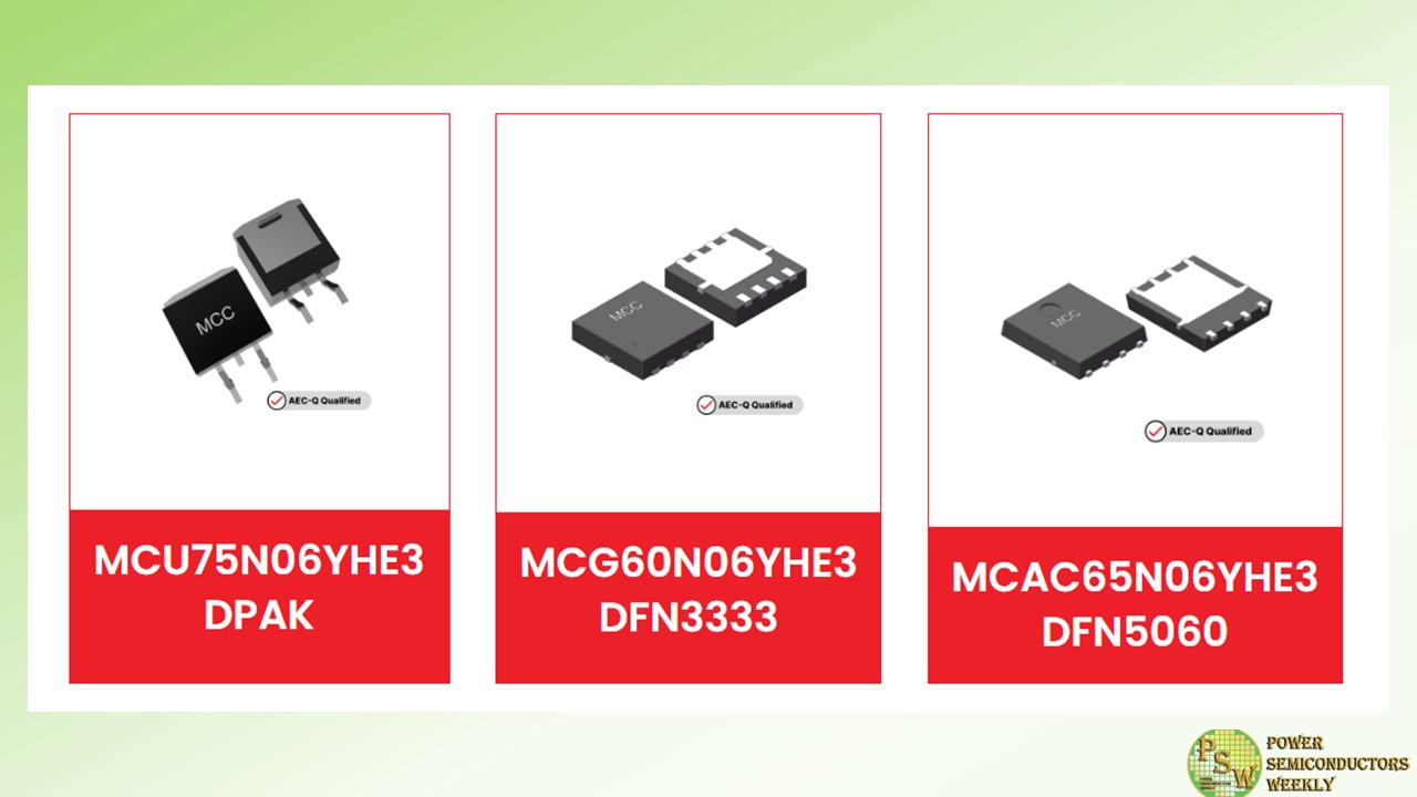
MCC Semi expanded its growing auto-grade portfolio with three new 60V N-channel MOSFETs: MCU75N06YHE3-TP, MCG60N06YHE3-TP, and MCAC65N06YHE3-TP.
Leveraging split-gate trench (SGT) MOSFET technology, MCC’s new products deliver optimal performance, efficiency, and thermal management, making them the intelligent choice for a range of demanding auto applications.
With on-resistance as low as 4.8mΩ, these AEC-Q101 qualified MOSFETs guarantee optimal power flow while significantly reducing power losses.
DFN333, DFN5060, and DPAK package options enable design flexibility and compatibility with various automotive systems.
Original – Micro Commercial Components
-
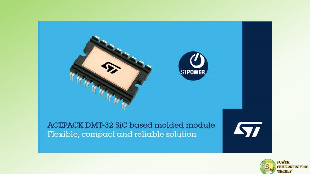
STMicroelectronics has released the ACEPACK DMT-32 family of silicon carbide (SiC) power modules in a convenient 32-pin, dual-inline, molded, through-hole package for automotive applications. Targeted at systems such as on-board chargers (OBC), DC/DC converters, fluid pumps and air conditioning, they deliver advantages including high power density, very compact design, and simplified assembly. The product family enhances flexibility for system designers by presenting a choice of four-pack, six-pack, and totem-pole configurations.
The modules contain 1200V SiC power switches that leverage ST’s state-of-the-art, second- and third-generation SiC MOSFET technology ensuring low RDS(on) values. The devices deliver efficient switching performance with minimal dependence on temperature to ensure high efficiency and reliability at converter system level.
Leveraging ST’s proven, robust ACEPACK technology, the modules reduce overall system- and design-development costs while ensuring outstanding reliability. The package technology features a high-performance aluminum nitride (AlN) insulated substrate for excellent thermal performance. There is also an integrated NTC sensor that provides temperature monitoring for thermal protection.
The first product in ACEPACK DMT-32, introduced today with ramp-up to volume production since Q4’23, is M1F45M12W2-1LA. The M1F80M12W2-1LA, M1TP80M12W2-2LA, M1P45M12W2-1LA, M1P80M12W2-1LA, M1P30M12W3-1LA are sampling now with ramp-up to volume production starting from Q1’24.
Original – STMicroelectronics
-
Infineon Technologies AG announced the closing of the acquisition of GaN Systems Inc. (“GaN Systems”). The Ottawa-based company brings with it a broad portfolio of gallium nitride (GaN)-based power conversion solutions and leading-edge application know-how. All required regulatory clearances have been obtained and GaN Systems has become part of Infineon effective as of the closing.
“GaN technology is paving the way for more energy-efficient and CO 2-saving solutions that support decarbonization,” said Jochen Hanebeck, CEO of Infineon. “The acquisition of GaN Systems significantly accelerates our GaN roadmap and further strengthens Infineon’s leadership in power systems through mastery of all relevant power semiconductor technologies. We welcome our new colleagues from GaN Systems to Infineon.”
Infineon now has a total of 450 GaN experts and more than 350 GaN patent families, which expands the company’s leading position in power semiconductors and considerably speeds up time-to-market. Both companies’ complementary strengths in IP and application understanding as well as a well-filled customer project pipeline put Infineon in an excellent position to address various fast-growth applications.
On 2 March 2023, Infineon and GaN Systems announced that the companies had signed a definitive agreement under which Infineon would acquire GaN Systems for US$830 million. The acquisition, an all-cash transaction, was funded from existing liquidity.
Original – Infineon Technologies
-
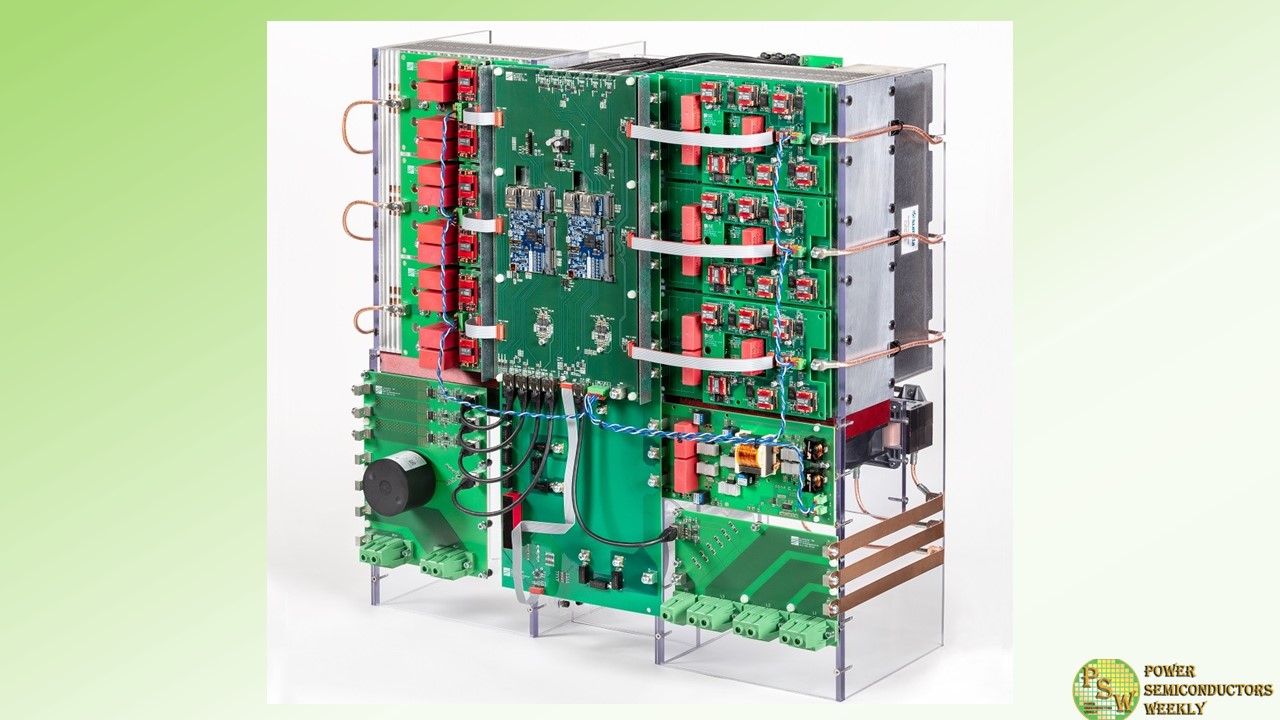
The Fraunhofer Institute for Solar Energy Systems ISE has developed and suc-cessfully commissioned the world’s first medium-voltage string inverter for large-scale power plants. By feeding power into the medium-voltage grid, the “MS-LeiKra” project team has demonstrated that PV inverters are technically capable of handling higher voltage levels.
The benefits for photovoltaics in-clude enormous cost and resource savings for passive components and cables. The device lays the foundation for a new system concept for the next genera-tion of large-scale PV power plants, which can also be applied to wind turbines, electric mobility and industrial applications.
Modern PV string inverters have an output voltage of between 400 VAC and 800 VAC. Although the output of power plants is steadily growing, voltage has not yet been increased. There are two reasons for this: First, building a highly efficient and compact inverter based on silicon semiconductors is a challenge. Second, there are currently no PV-specific standards that cover only the low-voltage range (max. 1,500 VDC / 1,000 VAC).
In a project funded by the German Federal Ministry for Economic Affairs and Climate Action (BMWK), Fraunhofer ISE, in collaboration with Siemens and Sumida, has developed an inverter that enables the output voltage to be increased to the medium-voltage range (1,500 V) at 250 kVA. The key to this is the use of silicon carbide semiconductors, which have a higher blocking voltage.
The research team has also implemented a more efficient cooling concept using heat pipes, which reduces the amount of aluminum required.
Thinner cables offer huge savings potential
An average photovoltaic power plant requires dozens of kilometers of copper cables. Increasing the voltage generates significant savings potential: At today’s possible output voltage of 800 VAC, a 250 kVA string inverter requires cables with a minimum cross section of 120 mm². By increasing the voltage to 1,500 VAC, the cable cross section can be reduced to 35 mm².
This in turn cuts copper consumption by around 700 kilograms per kilometer of cable. “Our resource analyses show that in the medium term, the electrification of the energy system will lead to copper becoming scarce. Increasing the voltage allows us to save valuable resources,” says Prof. Dr. Andreas Bett, Director of the Fraunhofer Institute for Solar Energy Systems ISE.
Standards need to change
With the “MS LeiKra” project, we are leaving the scope of low-voltage (<1000 VAC / <1500 VDC) standards. There are currently no PV-specific standards for this range. This is why the project team is also working on the standards that would result from increasing the voltage.
Finding a demo project partner
Having fed power into the medium-voltage grid successfully, the research team is now looking for solar farm developers and grid operators to test the power plant concept in the field.
Besides photovoltaics, moving beyond low voltage is also of interest for other applications, such as wind turbines, where the growing system capacities also require cables with large cross sections. The same is true for the charging infrastructure for large electric vehicles and vehicle fleets, and for industrial grids, where medium-voltage inverters could save a lot of material if cable cross sections could be reduced.
Original – Fraunhofer ISE
-
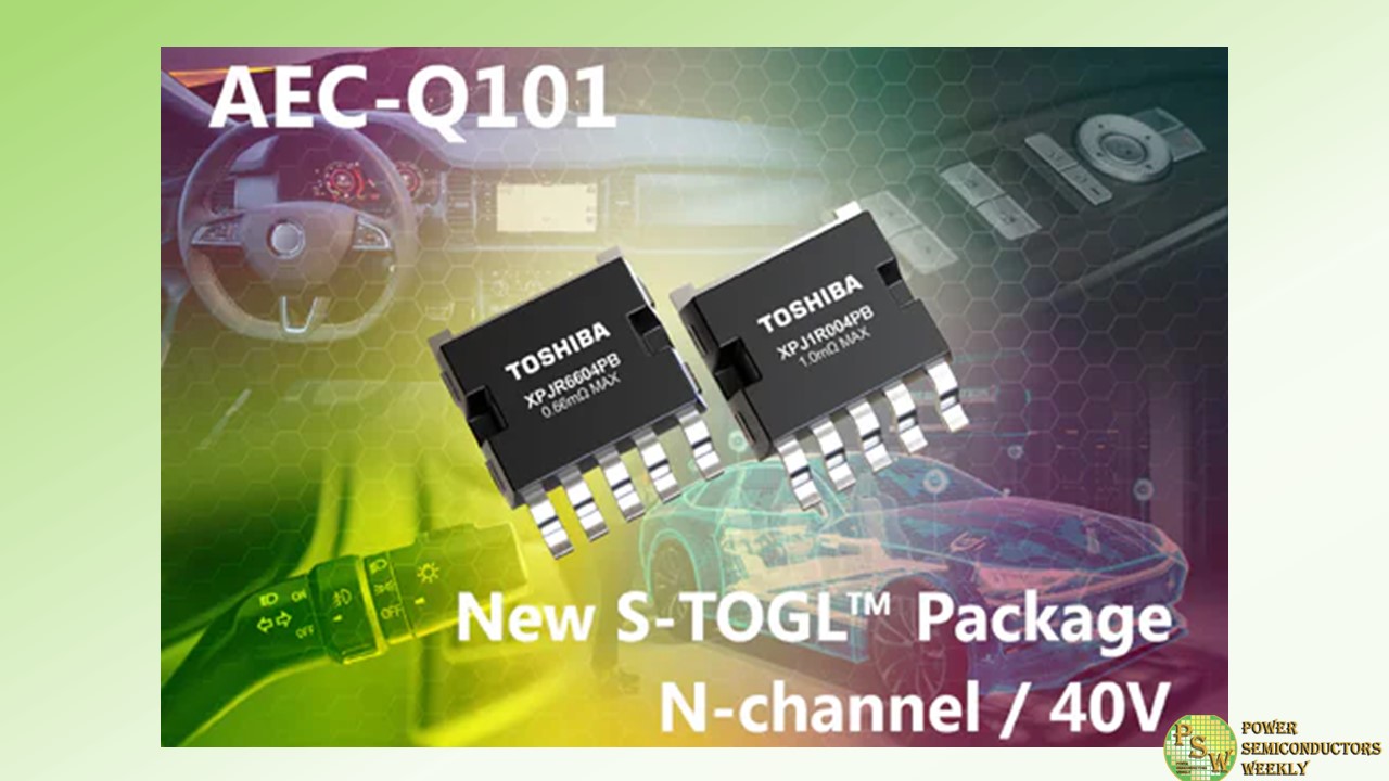
Toshiba Electronics Europe GmbH has launched a pair of automotive grade 40V N-channel power MOSFETs based upon their latest U-MOS IX-H process. The new devices use a new S-TOGLTM (Small Transistor Outline Gull-wing Leads) package that offers a number of advantages in automotive applications.
Automotive safety-critical applications such as steering, braking and autonomous driving systems generally require more devices than other systems to meet redundancy requirements. Here, a power MOSFET with high current density is required due to the size constraints within automotive equipment.
The new XPJR6604PB and XPJ1R004PB have a VDSS rating of 40V and the XPJR6604PB is rated for a continuous drain current (ID) of 200A (XPJ1R004PB = 160A). Both devices are rated for pulsed current (IDP) at 3x this value, 600A and 480A respectively. The 200A rating is higher than that achieved by Toshiba’s 6.5mm × 9.5mm DPAK+ package.
The new XPJR6604PB and XPJ1R004PB automotive MOSFETs use Toshiba’s innovative new S-TOGLTM package that measures just 7.0mm × 8.44mm × 2.3mm. The products are post-less and feature a multi-pin structure for the source leads that significantly decreases package resistance.
Combining the S-TOGLTM package with Toshiba’s U-MOS IX-H process gives the XPJR6604PB an on-resistance (RDS(ON) Compared to this device, the mounting area has reduced by around 55% compared while retaining the channel-to-case thermal resistance characteristics (Zth(ch-c)) – XPJR6604PB = 0.4ºC/W and XPJ1R004PB = 0.67ºC/W.
Many automotive applications are based in severely harsh environments, so the reliability of surface mount solder joints is a critical consideration. Toshiba’s S-TOGLTM package uses gull-wing leads that reduce mounting stress, improving the reliability of the solder joint.
Suited to harsh temperature environments, the MOSFETs are AEC-Q101 qualified and capable of operating at channel temperatures (Tch) as high as 175ºC.
Toshiba offers matched shipments for the devices, in which the gate threshold voltage range does not exceed 0.4V for each reel. This facilitates designs with small characteristic variations for applications requiring parallel connectivity for high-current operation.
Original – Toshiba
-

onsemi announced the completed expansion of its state-of-the-art, world-largest silicon carbide (SiC) fabrication facility in Bucheon, South Korea. At full capacity, this fab will be able to manufacture more than one million 200 mm SiC wafers per year.
To support the ramp in SiC manufacturing capacity, onsemi plans to hire up to 1,000 local employees over the next three years to fill the mostly highly technical positions – a more than 40% increase over the present workforce of about 2,300.
Silicon carbide devices are a critical component for power conversion in electric vehicles (EVs), energy infrastructure and high-power EV chargers. The rapidly growing demand for these products has created a surge in demand for SiC chips, with demand outpacing supply for the foreseeable future. The expansion of the Bucheon fab addresses the pressing need for additional production capacity, allowing onsemi to continue to provide supply assurance for its customers and strengthen its leadership in intelligent power solutions.
Construction of the new advanced 150 mm/200 mm SiC fab line along with the high-tech utility building and adjacent parking garage began in the middle of 2022 and was completed in September 2023. The expansion of the 150 mm/200 mm SiC Epi and wafer fab emphasizes onsemi’s focus on building out its vertically integrated silicon carbide manufacturing supply chain at brownfield locations. The Bucheon SiC line is starting with the production of 150 mm wafers and will be converted to 200 mm in 2025 upon qualification of the 200 mm SiC process.
onsemi’s leadership was joined by a delegation of dignitaries led by Vice Governor for Economy of the Gyeonggi-Do Taeyoung Yeom; followed by Bucheon City Mayor YongEek Cho; National Assembly delegates; and Bucheon Chamber of Commerce and Industry Chairman JongHuem Kim. Also in attendance were representatives from local communities, customers, suppliers and the semiconductor industry.
onsemi CEO Hassane El-Khoury opened the event, noting, “The 150 mm/200 mm SiC wafer fab in Bucheon is critical to the continued success of our fully integrated SiC supply chain, enabling us to support the acceleration of electrification globally. The last five years have shown what extraordinary performance our Bucheon team is capable of, and what we can achieve when we work together with governmental agencies toward the common goal of a more sustainable future.”
“I am truly impressed by onsemi’s diligent and yet fast execution of its strategic plan to expand the Bucheon SiC wafer fab,” said Bucheon City Mayor YongEek Cho. “Not only will the city of Bucheon benefit from the creation of new employment opportunities in technology, but it will also be a part of laying the foundation for a sustainable ecosystem through electrification.”
Original – onsemi
-
Mitsubishi Electric Corporation announced that it played the key role in leading the project to draft the 2023 International Electrotechnical Commission (IEC) White Paper entitled “Power Semiconductors for an Energy-Wise society,” which the IEC released on October 17. This is the first time for a White Paper, published annually since 2010, to issue recommendations for developing and expanding international standards and certification systems for power semiconductors.
Each year, the IEC White Paper focuses on electrical, electronic and electromechanical technologies requiring international standardization, and makes related recommendations to the IEC and other organizations.
Power semiconductors, one of Mitsubishi Electric’s core product lines, are expected to continue to advance technologically and be increasingly adopted as key devices that reduce power consumption and efficiently convert electrical energy, supporting the global drive toward carbon neutrality by 2050.
New materials such as silicon carbide (SiC) are being used in advanced power semiconductors for applications such as renewable energy and electric vehicles (EVs), but the development of international standards and certification systems for such devices is lagging. A lack of such standards and certifications could lead to a proliferation of nonconforming products and impede cooperation among manufacturers, users and regulators, thereby hindering the healthy growth of the power semiconductor global market.
In response, Mitsubishi Electric initiated a White Paper project within the IEC Market Strategy Board (MSB) in October 2022. Together with experts from around the world, the project team addressed issues related to power semiconductor technologies, markets, and regulations.
The resulting White Paper summarizes the applications, sectors and technological trends of power semiconductors and highlights the need for the development, alignment, and expansion of respective international standards and certification systems. In particular, the White Paper focuses on the critical role that power semiconductor standards can play in helping to realize emission-free, carbon-neutral industries for a healthier and more prosperous world.
The main points of the 2023 IEC White Paper include:
- Current status and future trends of society, markets, and technologies related to power semiconductors and applications that are essential for realizing an “Energy-Wise society” in which energy is used wisely and efficiently.
- Challenges facing the power semiconductor industry and solutions for achieving carbon neutrality by 2050 through an integrated approach involving relevant regulatory, industry and international standardization organizations around the globe.
- Recommendations for international standardization bodies, particularly the IEC, to establish a roadmap and guidelines for the development of international standards and conformity assessment systems for power semiconductors.
The White Paper project team was led by Dr. Kazuhiko Tsutsumi, Mitsubishi Electric’s specially appointed technical advisor who also serves as IEC Vice President and Chair of the MSB, and included experts from Mitsubishi Electric’s Corporate Intellectual Property Division (Tokyo), Mitsubishi Electric’s Power Device Works (Fukuoka), Mitsubishi Electric Europe B.V. German Branch (Ratingen, Germany), as well as a team of international experts.
Going forward, Mitsubishi Electric will collaborate with power semiconductor companies, users, and regulatory authorities to establish a roadmap for the creation of power semiconductor international standards as recommended in the 2023 IEC White Paper, with the aim of promoting the healthy growth of the power semiconductor market in the quest for carbon neutrality by 2050.
Original – Mitsubishi Electric
-
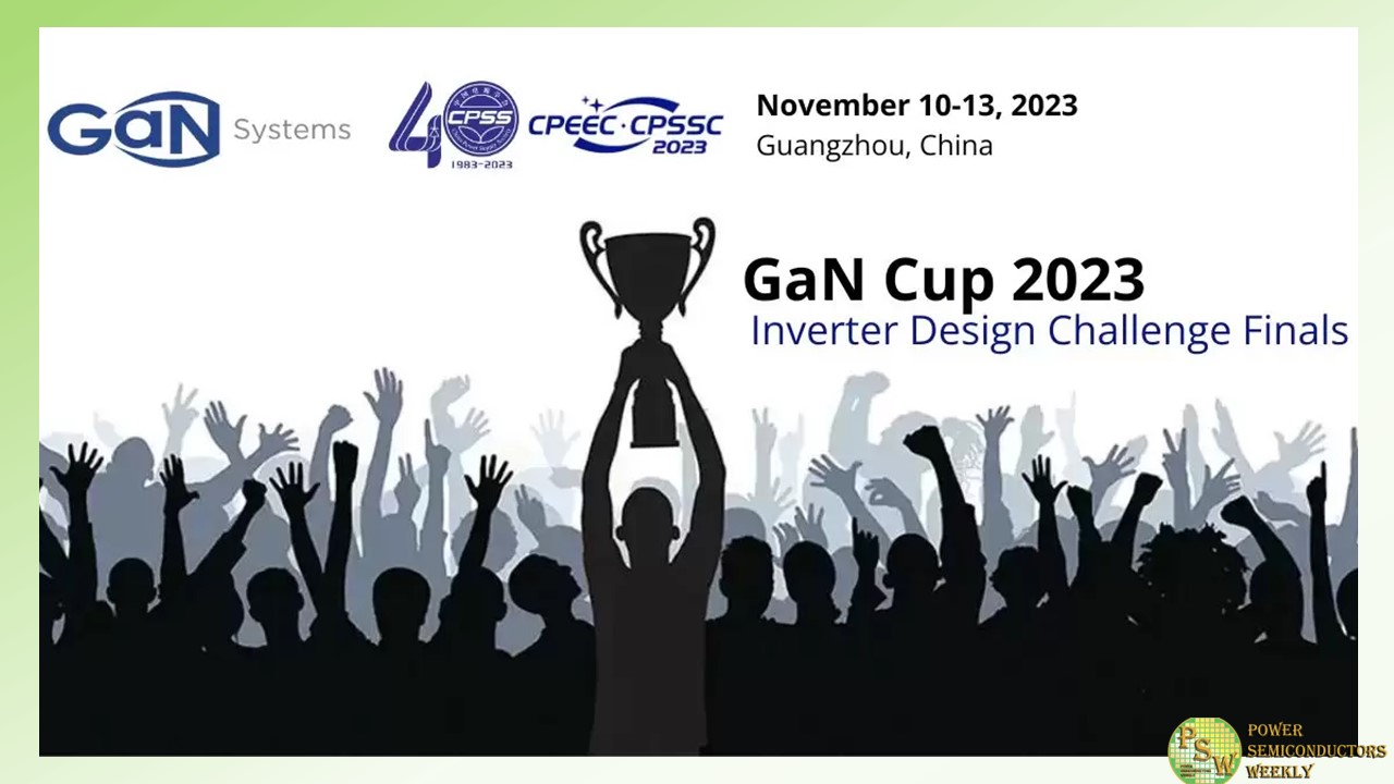
GaN Systems announced that it will demonstrate the latest breakthroughs of GaN for sustainable and cost-effective power designs at the 2023 China Power Electronics and Energy Conversion Congress and the 26th China Power Supply Society Annual Conference & Exhibition (CPEEC & CPSSC 2023), taking place on November 10-13, 2023, in Guangzhou, China.
Finals of the Annual “GaN Systems Cup” Power Electronics Application Design Competition will kick off concurrently. GaN Systems, as the primary sponsor for nine consecutive years, will participate in the opening ceremony and recognize the winners at the award ceremony.
While power efficiency is at the forefront of global policymaking, advancements in power electronics have gained importance, and talent remains the cornerstone of these advancements. The “GaN Systems Cup” Competition provides a podium for aspiring young engineers to challenge themselves and unlock the full potential of power electronics with GaN power semiconductors.
This year, out of the 68 teams from 46 colleges and universities that participated, 24 qualify for finals. The finalists will present prototype designs for a three-phase inverter using GaN Systems’ power transistors. The panel of judges comprised of experts from the industry and academia will evaluate these prototype designs based on performance in efficiency and power density.
Explore New Opportunities for Power Electronics at the CPEEC & CPSSC 2023
GaN Systems will showcase the latest reference designs for automotive, data center, and consumer industries at Booth 3-026. Its representatives will also be available to discuss the step-function performance boost and industry-leading figures of merit of recently released Gen4 power platform.
Original – GaN Systems
