-

Texas Instruments Incorporated (TI) reported third quarter revenue of $4.53 billion, net income of $1.71 billion and earnings per share of $1.85. Earnings per share included a 5-cent benefit for items that were not in the company’s original guidance.
Regarding the company’s performance and returns to shareholders, Haviv Ilan, TI’s president and CEO, made the following comments:
- “Revenue was flat sequentially and decreased 14% from the same quarter a year ago. During the quarter, automotive growth continued and industrial weakness broadened.
- “Our cash flow from operations of $6.5 billion for the trailing 12 months again underscored the strength of our business model, the quality of our product portfolio and the benefit of 300-mm production. Free cash flow for the same period was $1.6 billion.
- “Over the past 12 months we invested $3.7 billion in R&D and SG&A, invested $4.9 billion in capital expenditures and returned $5.6 billion to owners.
- “TI’s fourth quarter outlook is for revenue in the range of $3.93 billion to $4.27 billion and earnings per share between $1.35 and $1.57. We continue to expect our 2023 effective tax rate to be about 13% to 14%.”
Original – Texas Instruments
-

Wolfspeed, Inc. announced that Thomas Werner, a board member since 2006, has been elected the new Chairman of the Board, effective immediately. Werner succeeds Darren Jackson, who stepped down as chair after five years in the role. Jackson will continue to serve as a member of the Wolfspeed Board. In addition, Board Member Stacy Smith will replace John Replogle as the Chair of the Governance and Nominations Committee.
“Wolfspeed is thrilled to welcome Tom as our new Board Chair,” said Gregg Lowe, Wolfspeed President & CEO. “Tom is a proven innovator with vast experience in the energy and semiconductor industries, and will provide invaluable leadership as we further scale our operations to meet the growing demand for silicon carbide power devices.”“It is my honor to serve as Wolfspeed’s Board Chair, and help Wolfspeed as it leads the transition from silicon to silicon carbide,” said Werner. “Wolfspeed is on the cusp of truly changing the power electronics industry, and I am excited to be a part of that transformation.”
Werner is a distinguished industry leader with more than 25 years of experience in semiconductor, disruptive technology and energy organizations. Werner previously served as the Chairman of the Board of Directors for SunPower Corporation, a publicly traded manufacturer and marketer of high-efficiency solar cells and solar panels, after serving as the Chief Executive Officer of SunPower for 18 years.
Smith is the Executive Chairman of Kioxia Corporation (formerly Toshiba Memory Corporation), a leading flash memory company, and Non-Executive Chair of the Board at Autodesk, Inc., a global leader in design and make technology. Prior to his Board positions, Mr. Smith worked at Intel Corporation for three decades in a variety of roles including as Group President of Sales, Manufacturing and Operations, Chief Financial Officer, Chief Information Officer, and Head of Europe Middle East and Africa.
Original – Wolfspeed
-
GaN Valley™ is a connected ecosystem along the value chain of GaN technologies, products and electrical systems. It spans research and innovation (such as top-notch universities & RTOs), IDMs, Fabless Companies (including a growing industry of GaN start-ups & scale-ups), GaN Foundries, multi-market customers, as well as various Government Innovation instances.
Okmetic is now a part of GaN Valley™ community and looks forward to cooperation with other members in the GaN ecosystem!
Okmetic supplies substrate wafers for both RF and Power GaN devices. Its silicon substrate wafers are designed to endure the demanding GaN epitaxial process conditions and provide reduced wafer bow and warpage.
Original – Okmetic
-
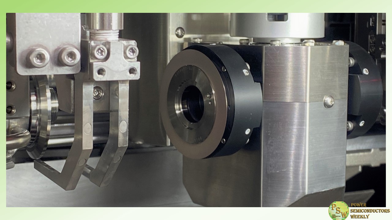
DISCO Corporation has developed a new ABC (Auto Blade Changer) that can automatically replace hubless blades as an optional function, and it is currently available for purchase. This function is planned to be exhibited at SEMICON Japan 2023 (December 13 – 15, Tokyo Big Sight).
Developmental Background
Dicing saws were originally developed to singulate fully-manufactured semiconductor wafers, but in recent years, dicing saws are also being used in applications such as package dicing following resin molding (QFN packages, etc.), passive component dicing such as condensers and inductors, and dicing optical parts that use glass.
When dicing silicon wafers, the blade used is called a hub blade, and it is attached to an aluminum hub. The Auto Blade Changer (ABC), an automatic replacement function for these hub blades, was developed and has been sold by DISCO since 2005, and has contributed to the improved productivity of the dicing process and the reduction of human errors.
However, manual replacement by an operator was necessary to replace hubless blades that are widely used in applications such as package dicing as mentioned above. This newly developed ABC supports both hubless and hub blades, enabling automatic replacement regardless of the blade type.Features
The new ABC supports blade replacement of both hubless and hub blades.
- Improves operation rates
- Reduces downtime caused by waiting for the operator
- Prevents human error
- Reads the blade ID using a QR code, and automatically fills in values such as the blade exposure
- Contributes to traceability
- Records the blade lot ID used
Supported models
The new ABC can currently be installed in the following three equipment models.
DFD6342:A facing dual spindle dicing saw that supports Φ200 mm wafers
DFD6561:A facing dual spindle dicing saw that supports Φ300 mm wafers
DFD6755:A facing dual spindle dicing saw with two chuck tables specialized for package dicingOriginal – DISCO
- Improves operation rates
-
In the world of electric vehicles (EVs), performance and efficiency are paramount. As the EV industry grows, power designers constantly strive to provide more power, reduce losses, minimize heat, and shrink system sizes. These requirements stem from the ongoing pursuit of lighter vehicles with extended ranges, reduced battery size, and lower overall system costs.
The continuous drive for improvement has led to accelerated adoption of a pivotal technology transforming the landscape of EV traction design: Gallium Nitride (GaN). Particularly noteworthy are the benefits of GaN in 400V and 800V battery traction inverter designs. The growing recognition of GaN’s exceptional performance, compared to conventional silicon and SiC alternatives, underscores its critical role in the future of the EV industry.
GaN-Powered 400V Battery Traction Inverters
GaN stands out as a transformative force for 400V battery-based traction inverters—delivering the benefits that designers expect. With GaN, efficiency increases, resulting in nearly 40% reduction in power loss. Additionally, GaN power semiconductors enable a 33% increase in power density, reducing the overall size and weight of the traction inverter. Altogether, the reduced losses and smaller size result in EVs with lower costs and longer driving range, meeting critical consumer requirements.
GaN’s Emergence in 800V Battery Traction Inverters
In 800V battery-based traction inverters, the adoption of GaN-based three-level topology (3LT) is a growing trend. The demonstrated benefits are numerous.
- Higher Overall Efficiency: In addition to minimizing switching losses and increasing efficiency in the inverter, the GaN 3LT solution also reduces high-frequency copper and iron losses in the filters and motor. The inverter plus motor combined efficiency gains translates to incrementally higher efficiency compared to two-level solutions.
- Lower Noise, Harshness, and EMI Interference: The GaN 3LT generates an output voltage with a sinusoidal-like shape, resulting in reduced dV/dt and lower harmonics. The 3LT output reduces filtering requirements and minimizes high-frequency losses in filters and motors, resulting in lower noise, vibration, and harshness (NVH) characteristics. It also operates with a low common voltage, reducing insulation stress and electromagnetic interference (EMI).
- Increased Durability and Reliability: Operating at a lower common voltage also means the peak common mode voltage is suppressed, which reduces the potential for common mode voltage spikes, ensuring a smoother and more stable circuit operation. Furthermore, the 3LT decreases the strain on electric motor bearings. These operating characteristics contribute to a prolonged lifespan with increased durability and reliability.
The EV Market
EVs are at their tipping point, with more than 10 million electric cars sold worldwide in 2022, and sales are expected to grow by 35% this year to reach 14 million cars. Meeting consumer, regulatory, and OEM expectations means peak performance is critical, and this requires a holistic approach that factors in both the inverter and motor considerations. Multi-level GaN is emerging as the lynchpin, offering a range of advantages. Notably, GaN fosters high efficiency at the system level while bolstering overall system reliability.
For example, consider the all-GaN vehicle developed in collaboration with Toyota and Nagoya University teams. The All GaN Vehicle features multiple power applications of GaN in the car: in the traction inverter, the On-Board Charger (OBC), and the DC-DC converter. GaN increased power density and improved efficiency by 20% over silicon, extending the car’s driving range.
Meanwhile, Ricardo, a highly regarded global engineering firm, designed and compared a GaN inverter to a SIC-based inverter. Their test results of the 30kW inverter application demonstrated a 25% reduction in power loss and a 33% increase in power density with GaN compared to SiC. Several Tier1 and OEM automotive companies have realized similar results with traction designs up to 250kW.
In an era of EV innovation, GaN is a driving force accelerating performance and efficiency in both 400V and 800V traction inverters. With the EV industry advancing towards worldwide mass acceptance, the time for GaN adoption is now. The compelling results from rigorous testing and real-world applications point to GaN as the technology well-positioned to reshape the electric mobility landscape.
Original – GaN Systems
-
Navitas Semiconductor announced its continued sponsorship of the 2023 China Power Electronics and Energy Conversion Congress & the 26th China Power Supply Society (CPSS) Conference and Exhibition (CPSSC 2023), revealing major next-generation gallium nitride (GaN) and silicon carbide (SiC) power semiconductor platforms, including GaNSafe™ – the world’s safest GaN power semiconductor.
Hosted in Guangzhou from November 10th-13th, CPSSC 2023 celebrates its 40th anniversary and promotes academic and technical exchange in the fields of power electronics, energy conversion, and power technology, to foster technical innovation and related industries.
Navitas is the technology and market leader in GaN, with over 100 million GaNFast™ power ICs shipped, and over 12 million GeneSiC™ power MOSFETs and diodes shipped into a $22 billion per year total market opportunity.
With GaNSafe, Navitas has optimized its 4th-generation GaN technology for demanding, high-power applications in data centers, solar / energy storage and EV markets, where efficiency, power density and robust & reliable operation are critical. Adopting a novel, robust, and cool-running surface-mount TOLL package, GaNSafe integrates features and functions, including:
- Protected, regulated, integrated gate-drive control, with zero gate-source loop inductance for reliable high-speed 2 MHz switching to maximize power density.
- High-speed short-circuit protection, with autonomous ‘detect and protect’ within 50 ns – 4x faster than competing discrete solutions.
- Electrostatic discharge (ESD) protection of 2 kV, vs. zero for discrete GaN transistors.
- 650/ 800 V capability to aid survival during extraordinary application conditions.
- Easy-to-use, complete, high-power, high-reliability, high-performance power IC with only 4 pins, accelerating customer designs.
- Programmable turn-on and turn-off (dV/dt) to simplify EMI regulatory requirements.
Navitas’ CPSSC 2023 program includes comprehensive, in-depth technology, application and market presentations include a plenary keynote speech, full conference paper, four industrial sessions, a guest PSMA presentation, an in-depth 3.5-hour technology seminar and full GaNSafe launch. Visitors to the exhibition will discover ground-breaking technology demonstrations and complete power system platform designs at the Navitas booth.
Original – Navitas Semiconductor
-
 LATEST NEWS / PROJECTS / TOP STORIES
Samsung Electronics to Provide Service Across a Variety of Solutions, Including Power Semiconductors
October 19, 2023
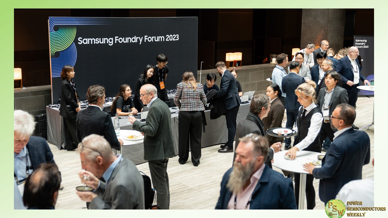
3 Min ReadSamsung Electronics hosted Samsung Foundry Forum (SFF) 2023 Europe and unveiled its advanced and wide ranging automotive process solutions, from the most advanced 2-nanometer process to the 8-inch legacy process.
Alongside its customers and Samsung Advanced Foundry Ecosystem (SAFE) partners, Samsung Electronics showcased the latest technological trends and its business strategy tailored to the European market.
“Samsung Foundry is driving innovation in next-generation solutions to build an expanded portfolio that meets the growing needs of our automotive customers, especially as the era of electric vehicles becomes a reality,” said Dr. Siyoung Choi, President and Head of Foundry Business at Samsung Electronics. “We are strengthening our readiness to provide customers with distinguished service across a variety of solutions, including power semiconductors, microcontrollers and advanced AI chips for autonomous driving.”
Since participating in IAA Mobility 2023 for the first time in September, Samsung Electronics is strengthening engagement and partnership in specialty processes for automotive customers in the European market, further solidifying its status as a leading foundry partner for the industry.
Pioneering New Applications With Industry’s Most Advanced eMRAM
In order to meet the needs of the latest advancements in the automotive market, Samsung is setting out to develop the industry’s first 5-nanometer eMRAM for next-generation automotive technology. eMRAM is a next-generation memory semiconductor used for automotive applications that enables high read and write speeds as well as superior heat resistance.
Since developing and mass producing the industry’s first 28nm FD-SOI based eMRAM in 2019, Samsung Electronics has been developing 14nm for the FinFET process based on AEC-Q100 Grade 1. Samsung Foundry plans to expand its eMRAM portfolio by adding 14nm by 2024, 8nm by 2026, and 5nm by 2027.
Samsung’s 8nm eMRAM shows potential to deliver a 30% increase in density and 33% increase in speed, compared to the 14nm process.
Tackling the Market With Automotive Process Solutions From Cutting-Edge to Legacy
The company announced its advanced process roadmap, highlighting its plans to complete mass production readiness for its 2nm process for automotive applications by 2026.
Samsung Electronics is also bolstering its readiness to serve customer needs by expanding its 8-inch BCD (Bipolar-CMOS-DMOS) process portfolio. The BCD process combines the strengths of three different process technologies: Bipolar (B), CMOS (C), and DMOS (D) on one chip and is most commonly used in the production of power semiconductors.
Samsung Electronics plans to expand its current 130nm automotive BCD process to add 90nm by 2025. The 90nm BCD process is expected to bring a 20% decrease in chip area compared to the 130nm process.
Implementing Deep Trench Isolation (DTI) technology, which reduces the distance between each transistor to maximize the performance of power semiconductors, Samsung Foundry will be able to apply a greater voltage of 120V instead of 70V to a wider range of applications. This will enable readiness to provide a process development kit (PDK) that implements 120V to the 130nm BCD process by 2025.
Leading ‘Beyond-Moore’ Innovation Through Advanced Packaging Alliance
Samsung established a Multi-Die Integration (MDI) Alliance by collaborating with its SAFE partners as well as major players in memory, package substrate, and testing.
As part of an industry-wide partnership with 20 partners, Samsung is leading the development of 2.5D and 3D packaging solutions customized for all applications from automotive to high-performance computing (HPC).
Samsung Electronics hosted the annual Samsung Foundry Forum 2023 in the United States on June 27-28, in South Korea on July 4, and in Japan on October 17. The content from the forum will be available on the Samsung Semiconductor website for worldwide access to all visitors beginning November 2.
Original – Samsung Electronics
-

Ardian, a world-leading private investment house, announced that it is expanding into semiconductor investment with the launch of Ardian Semiconductor. This innovative platform will invest across the semiconductor value chain with a focus on Europe and will enable companies to grow into global leaders in their markets.
Semiconductor devices are pervasive in the world economy and are the critical enablers of the digital transformation and green transition of key sectors, such as data infrastructure, mobility, industrial and consumer. Following several decades of consistent mid to high single digit growth, industry analysts believe the semiconductor industry will continue to grow and reach $1 trillion by 2030, driven by predictable megatrends such as artificial intelligence, cloud computing, electrification and automation of mobility and industry, or smart & connected devices.
Europe is one of the most attractive regions to invest in the coming decade. European companies in the value chain are global leaders in semiconductors for the mobility and industrial end-markets that are experiencing rapid technological transformation and expected to grow the fastest.
Europe also leads through its innovation ecosystems, IP, specialized equipment and materials companies, that underpin major megatrends such as the artificial intelligence revolution. Europe leverages strong foundations and attractive government incentives, including the €43 billion European Chips Act, to strengthen its leadership and benefit from an increased regionalization of the global supply chain.
Ardian Semiconductor aims at becoming the partner of choice of the European semiconductor value chain, bringing innovative and flexible capital solutions, as well as strategic and operational expertise, to companies with the potential to enable megatrends leveraging their distinctive technologies.
Ardian is launching the Ardian Semiconductor platform through an exclusive strategic partnership with Silian Partners, a team of highly successful senior executives from the semiconductor industry with more than 115 years of combined experience in the space, bringing unique industry relationships, strategic vision, and operational focus. Ardian and Silian Partners will work as One Team, and will bring together Ardian’s proven and successful private equity capabilities and investment processes with unparalleled industry leadership and expertise.
Ardian Semiconductor is managed by Ardian France. Silian Partners assists Ardian as an industry expert.
Ardian Semiconductor will be powered by a detailed analysis of technology megatrends and their implications across the semiconductor value chain. The team will work together to identify attractive opportunities, carry out expert due diligence, and work closely with entrepreneurs and management teams to define strategic roadmaps and execute.
This expansion builds on Ardian’s track record of investing in attractive high-growth sectors, in addition to its flagship investment activities.
“Semiconductors are everywhere and enable the world’s digital transformation and green transition. As demand for semiconductors is expected to more than double over the next decade, a whole supply chain needs to scale and bring continued innovation, including countless European mid-sized companies. We’re assembling a unique team with tremendous experience and track-record, and I can’t enjoy more than welcoming Paul, Christophe, Helmut and Thomas.
It’s therefore the perfect time to launch Ardian Semiconductor, leveraging Europe’s leading positions in critical segments of the semiconductor value chain. Building on Ardian’s proven track record as a global private investment leader, the platform will bring innovative capital solutions to this strategic value chain at a pivotal moment, working alongside world-class industry leaders.” Thibault Basquin, Member of the Executive Committee, Ardian
“We are delighted to partner with Ardian, who perfectly understand the unique opportunity to address a critical need of the European semiconductor value chain and become its financial sponsor of choice. Through a bespoke strategic partnership, we bring together in One Team seasoned private equity investors, proven investment processes, and successful semiconductor leaders.
Ardian is the ideal firm with the right people and culture to build this first-of-its-kind investment platform together. As we initiate dialogues with companies and entrepreneurs, we have confirmation that we enable solutions for the industry that do not exist today and that our approach will create significant value across the board.” Paul Boudre, Senior Managing Director & Co-Founder of Silian Partners
Silian Partners is led by:
- Paul Boudre, Senior Managing Director & Co-Founder, who brings c.35 years of semiconductor experience. As Chief Executive Officer of Soitec from 2015 to 2022, he successfully led the company through a restructuring and positioned it as a global leader of engineered semiconductor materials. Prior to Soitec, he held senior positions in semiconductor equipment and manufacturing with KLA, STMicroelectronics, IBM Microelectronics, Motorola Semiconductor and Atmel.
- Christophe Duverne, Senior Managing Director & Co-Founder, who has been a semiconductor and electronics executive for the past c.30 years. He was President and Chief Executive Officer of Linxens from 2010 to 2020, which he founded from a corporate carve-out, and led through two successful buyout transactions sponsored by CVC, Astorg and Bain Capital, to create a global leader in smart card components manufacturing. Prior to founding Linxens, he worked for over 10 years at NXP Semiconductors where he was Senior Vice President of the Identification business unit.
- Dr Helmut Gassel, Senior Managing Director & Co-Founder, who contributes c.30 years of semiconductor industry experience. He served as a member of Infineon’s Management Board as Chief Marketing Officer from 2016 to 2022 with responsibilities encompassing marketing, sales, strategy and M&A. In this capacity, he led the €9bn acquisition and integration of Cypress Semiconductor and contributed to transform Infineon into a global top 10 semiconductor company. Prior to joining Infineon in 1995 as a semiconductor design engineer, he worked in semiconductor research at Fraunhofer Institute
- Thomas Pebay-Peyroula, Managing Director & Co-Founder, who brings c.15 years of investment banking experience and has advised many European semiconductor companies on strategic, M&A and financing matters. He is joining from Rothschild & Co, and started his career with Lazard.
Original – Ardian
-
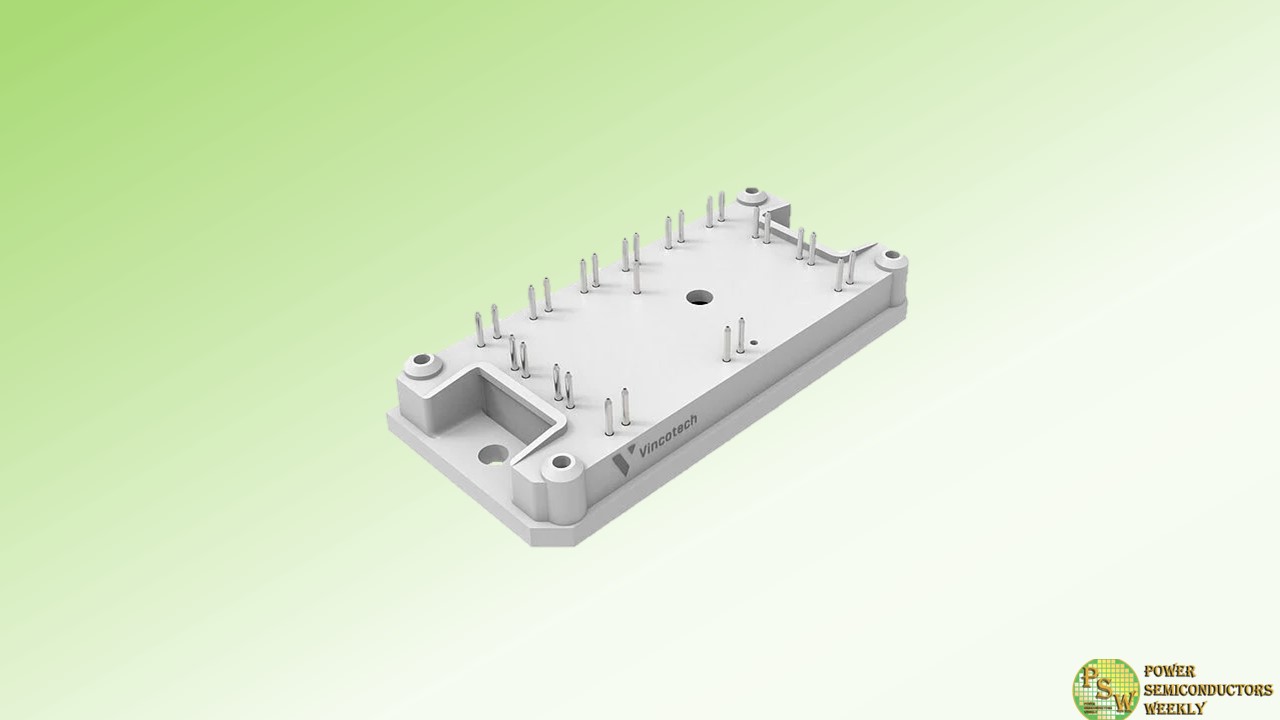
Designing state-of-the-art heat pumps and HVAC systems is not easy. Finding a way to overcome demands, such as giving more power in a smaller footprint requires a lot from a power module.
Vincotech’s new 1200 V PIM+PFC is the answer. Its integrated three-phase ANPFC and inverter stage resolve contradiction to boost efficiency and cut systems costs. More compact designs at higher power ranges is not a problem any more.
Samples are available through our usual channels.
Main benefits
- All-in-one solution: 3-phase PFC with inverter stage in a compact flow1 housing allows for more compact designs and higher power density
- High efficient AN-PFC topology with SiC diodes for switching frequencies up to 150 kHz reduces systems costs
- High speed IGBT’s in the inverter stage for high switching frequency operation
- Thin Al2O3 substrate eases the system’s thermal design
- Integrated thermal sensor simplifies temperature measurement
Applications
- Embedded drives
- Industrial drives
Original – Vincotech
-
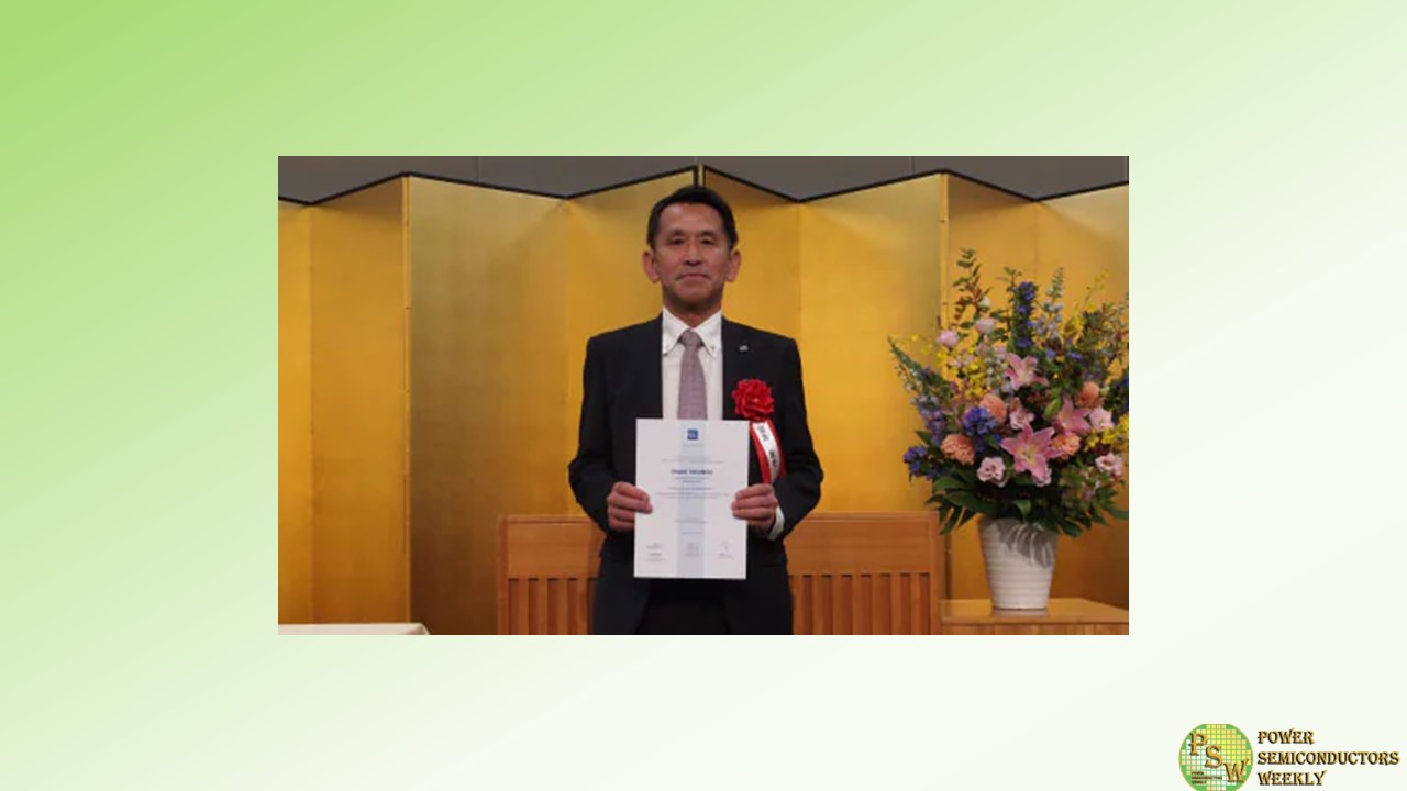
Toshiba Electronic Devices & Storage Corporation announced that Atsushi Tomishima, an Expert at its Electronic Devices & Storage Research & Development (R&D) Center, is a recipient of a 2023 1906 Award from the International Electrotechnical Commission (IEC).
The IEC is the world leader in evaluating and publishing international standards for electrical, electronic, and related technologies. The 1906 Award, created in 2006 and named for the year IEC was founded, honors the work of experts around the world whose work is fundamental to IEC and the execution of its important mission. The Award also recognizes recent and exceptional achievements—a project or other contribution—related to IEC’s activities that contribute in a significant way to advancing the Commission’s work.
Mr. Tomishima, a researcher in the Package Solution Technology Development Dept. at Toshiba’s Electronic Devices & Storage R&D Center, has been an expert member representing Japan on the IEC’s subcommittee on integrated circuit technology (TC47/SC47A) since FY2015. He also serves as an executive member of the electromagnetic compatibility (EMC) subcommittee of the Japan Electronics and Information Technology Industries Association, and has led the subcommittee’s activities, and consolidated numerous opinions and proposals on standardization.
At IEC’s EMC simulation modelling (SC47A WG2) and EMC measurement methods on Integrated circuit (WG9) working groups, he has elicited opinions from many countries, ensured a full understanding of each participant’s position, and summarized discussions.
Through these activities, he received this award in recognition of his significant contribution to the efficient promotion of standardization in the semiconductor design and testing field. These international standards established by Mr. Tomishima’s activities allow us to accurately evaluate the noise characteristics of semiconductors themselves, greatly contributing to improving the quality of product design such as integrated circuits and automobiles.
Toshiba will continue to promote international standardization activities in the electric and electronic technologies areas.
Original – Toshiba
