-

The accelerated transition to electric vehicles has led to significant innovations in charging systems that demand more cost-efficient and high performing power electronics. Addressing this, Infineon Technologies AG expands its 650 V CoolMOS™ CFD7A portfolio by introducing the QDPAK package.
This package family is designed to provide equivalent thermal capabilities with improved electrical performance over the well-known TO247 THD devices, thus enabling efficient energy utilization in onboard chargers and DC-DC converters.
Efficient and powerful electric vehicle charging systems help reduce charging times and vehicle weight, increasing design flexibility and reduce the total cost of ownership of the vehicle. This new addition complements the existing CoolMOS CFD7A series, offering versatility with top-side and bottom-side cooled packages. The QDPAK TSC (top side cooled), enables designers to achieve higher power densities and optimal PCB space utilization.
The 650 V CoolMOS CFD7A offers several important features for reliable operation in high-voltage applications. Thanks to its reduced parasitic source inductance, the device can minimize electromagnetic interference (EMI), ensuring clear signals and consistent performance.
The Kelvin source pin also provides improved precision for current sensing, ensuring accurate measurements even in challenging conditions. With a creepage distance suitable for high voltage applications, as well as high current capability and high power dissipation (P tot) of up to 694 W at 25°C, it is a versatile and powerful device for a wide range of high-voltage applications.
New system designs using 650 V CoolMOS CFD7A in QDPAK TSC will maximize PCB space use, doubling power density and enhancing thermal management via substrate thermal decoupling. This approach simplifies assembly, eliminates board stacking and reduces the need for connectors, thereby lowering system costs. The power switch reduces thermal resistance by up to 35 percent, providing high power dissipation that outperforms standard cooling solutions.
This feature overcomes the thermal limitations of bottom side cooled SMD designs using FR4 PCBs, resulting in a significant boost in system performance. The optimized power loop design locates drivers near the power switch, improving reliability by reducing stray inductance and chip temperatures. Overall, these features contribute to a cost-effective, robust, and efficient system ideal for modern power needs.
As announced in February 2023, the QDPAK TSC package has been registered as a JEDEC standard for high-power applications, helping to establish a broad adoption of TSC in new designs with one standard package design and footprint. To further to accelerate this transition, Infineon will also release additional Automotive Qualified devices in QDPAK TSC for onboard chargers and DC-DC converters in 2024, such as 750 V and 1200 V CoolSiC™ devices.
Original – Infineon Technologies
-
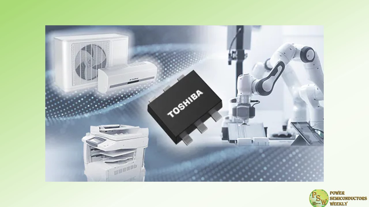
Toshiba Electronic Devices & Storage Corporation has launched the product “HN1D05FE”, a 400 V voltage switching diode. The new product “HN1D05FE” is suitable for applications that require high voltage characteristics such as commercial AC power supply circuits and AC-DC converter circuits for LED illumination. With a 400 V reverse voltage rating, HN1D05FE is suitable for power supply circuits below 200 V, as well as reverse-current protection and surge protection, and more.
In addition, the new product is housed in a SOT-563 package (Toshiba package name: ES6, 1.6 mm × 1.6 mm (typ.), t=0.55 mm (typ.)) to achieve high voltage characteristics in a small size.
Furthermore, built-in two switching diodes allow reducing the number of devices in circuits which use multiple devices.Moreover, the package size is reduced by approximately 70 % and the package height is as low as 50 % compared with the SOT-24 package (Toshiba package name: SMQ, 2.9 mm × 2.9 mm (typ.), t=1.1 mm (typ.)) of Toshiba’s existing product 1SS399. This helps to downsizing and thinning of the set.
Applications
- Consumer equipment (home appliances, OA equipment, PC, etc.)
- Industrial equipment (FA equipment, PV, semiconductor-manufacturing equipment, etc.)
Features
- High reverse voltage : VR = 400 V
- Low leakage current : IR = 0.1 μA (max) (VR = 400 V)
- Small and thin SOT-563 Package : Toshiba Package Name : ES6 (1.6 mm × 1.6 mm (typ.), t = 0.55 mm (typ.))
Original – Toshiba
-
Resonac Corporation will take part in a consortium of semiconductor-related manufacturers named “Texas Institute for Electronics”, which is located in the state of Texas, USA. Resonac will be the first Japanese member of TIE as a semiconductor material manufacturer.
TIE is a non-profit organization led by The University of Texas at Austin, and consists of the public and private sectors including the state of Texas, semiconductor manufacturers, defense electronics manufacturers, national laboratories, and academic bodies.
Its aim is to advance the roadmap of cutting-edge semiconductor systems by five years (or more than two generations), and to develop them in the United States.. TIE’s strategic member companies include leading semiconductor manufacturers such as AMD, Inc., Micron Technology, Inc., Intel Corporation, Applied Materials, Inc., etc.
Resonac was invited to participate as the strategic member from the materials manufacturers, as it was recognized by TIE for the comprehensive lineup of materials for the front-end and back-end processes used in advanced semiconductors, R&D organization specializing in semiconductor packaging “Packaging Solution Center,” and track record in operating the consortium “JOINT2” composed of semiconductor-related companies. TIE plans to launch a prototype line for wafer-scale 2xD and 3D advanced packaging starting from the second half of 2024.
Semiconductors support the lives of the people as social infrastructure. Development of leading-edge semiconductors to be used for AI and next-generation telecommunication requires cooperation between manufacturers of devices, materials, and equipment. Resonac will aim to cooperate with other companies through its participation in TIE, research and development of leading-edge technologies and contributions to solutions of problems concerning semiconductors.
Aiming to accomplish its purpose, “Change society through the power of chemistry,” Resonac will strive to promote co-creation, and contribute to improvement in semiconductors’ performance, which is needed by society.
Original – Resonac
-

AIXTRON SE enables the semiconductor foundry BelGaN to expand its business into the growing GaN marketand to accelerate GaN technology innovation. For this important strategic step, BelGaN relies on AIXTRON’s new G10-GaN, which offers best-in-class performance, an all-new compact design, and overall lowest cost per wafer.
Starting with an 8x150mm configuration, the system will be delivered to the BelGaN production site in Oudenaarde (Belgium) before the end of 2023 and will in the future migrate to 5x200mm.
BelGaN, a leading GaN (Gallium Nitride) automotive-qualified semiconductor open foundry in Europe, recently announced the production start of its first generation 650V eGaN technology. The Gen1 platform is designed for the requirements of energy-efficient applications for sustainability and carbon neutrality.
The G10-GaN will be used to further extend the range of power chips with voltage ratings from 40V to 1200V, using GaN-on-Si, GaN on SOI, and novel GaN-on-engineered substrates. It will be applied both on lateral as well as vertical power-GaN products, with a focus on high performance, automotive quality and reliability, high yield, and low costs.
“GaN-epitaxy using MOCVD is a most critical process in any power-GaN technology, both to innovate device architectures, boost performance, yield, and quality, and to cut down the cost of GaN products. This drives a paradigm shift in power electronics, opening up fast-growing markets in e-mobility, datacom, energy conversion, etc., on a road to an electrified, carbon-neutral society.
We have been impressed by the high levels of productivity, uniformity, and low cost of ownership of AIXTRON’s new G10 platform. We highly value AIXTRON’s technological advance, leadership, and continuous innovation. The proximity of AIXTRON, in the midst of the GaN ValleyTM ecosystem, and the collaboration with its team is essential for us to rapidly achieve our innovation and production objectives,” says Dr Marnix Tack, CTO and Vice President Business Development of BelGaN.
“We are very proud that BelGaN chose AIXTRON and our latest innovative powerhouse, the G10-GaN, for the important strategic milestone to add GaN epitaxy to its existing GaN processing line in Oudenaarde (Belgium). Currently, GaN power devices are rapidly adopted in a wide range of applications, and many customers are adding GaN capabilities to their silicon lines. We are excited that technology made by AIXTRON is facilitating this important transition,” says Dr. Felix Grawert, CEO and President of AIXTRON SE.
The all-new G10-GaN cluster solution builds on the fundamentals of AIXTRON’s current tool of record, the G5+ C, while extending each single performance metric:the new platform delivers twice the productivity per cleanroom area while enabling a new level of material uniformities, unlocking new levers of competitiveness for AIXTRON’s customers.
They benefit from more than 25% lowest cost of ownership than with any other equipment on the market today. The G10-GaN also guarantees the highest throughput per m2/cleanroom, and with its full automation end-to-end, it is the only MOCVD system fully designed for silicon fabs.
Original – AIXTRON
-
Resonac Holdings Corporation decided at its Board of Directors meeting on changes in corporate management (directors and audit & supervisory board members) as given below.
Kohei Morikawa (Representative Director; Chairman of the Board) will resign as Representative Director, and will be elected as Chairman of the Board at the Board of Directors meeting which is to be held after the General Meeting of Shareholders in late March 2024.
Keiichi Kamiguchi (Board Director; Managing Corporate Officer; Chief Risk Management Officer (CRO)) will resign as Board Director at the General Meeting of Shareholders in late March 2024. Kiyoshi Nishioka (Outside Board Director) will resign as Outside Board Director at the General Meeting of Shareholders in late March 2024.
Meanwhile, Nori Imai (Corporate Officer; Chief Human Resource Officer (CHRO)) will be elected as Board Director at the General Meeting of Shareholders in late March 2024. Kenji Yasukawa (Representative Director; Chairman of the Board, Astellas Pharma Inc.) will be elected as Outside Board Director of REH at the General Meeting of Shareholders in late March 2024.
Jun Tanaka (Audit & Supervisory Board Member) will resign as Audit & Supervisory Board Member at the General Meeting of Shareholders in late March 2024. Kiyomi Saito (Outside Member of Audit & Supervisory Board) will resign as Outside Member of Audit & Supervisory Board at the General Meeting of Shareholders in late March 2024.
Meanwhile, Mitsuo Katayose (Corporate Officer, Resonac Holdings Corporation; General Manager, High Performance Materials Business Headquarters, and General Manager, Life Science Business Headquarters, Resonac Corporation) will be elected as Audit & Supervisory Board Member, REH at the General Meeting of Shareholders in late March 2024.
Kiyoko Toda (former Vice President and Head of International Regulatory Compliance, Japan Branch, American Express International, Inc.) will be elected as Outside Member of Audit & Supervisory Board, REH at the General Meeting of Shareholders in late March 2024.
As of late March 2024, the Board of Directors will consist of Kohei Morikawa (Board Director; Chairman of the Board); Hidehito Takahashi (Representative Director; President and CEO); Hideki Somemiya (Board Director; Managing Corporate Officer; CFO); Tomomitsu Maoka (Board Director; Managing Corporate Officer; CSO/CRO); Nori Imai (Board Director; Managing Corporate Officer; CHRO); Kozo Isshiki, Noriko Morikawa, Tetsuo Tsuneishi, and Kenji Yasukawa (Outside Board Directors).
In addition, Toshiharu Kato will continue serving as Audit & Supervisory Board Member, while Mitsuo Katayose will serve as a newly elected Audit & Supervisory Board Member. Masako Yajima and Yasuyuki Miyasaka will continue serving as Outside Members of the Audit & Supervisory Board, while Kiyoko Toda will serve as a newly elected Outside Member of Audit & Supervisory Board.
Original – Resonac
-

Analog Devices, Inc. announced financial results for its fourth quarter and fiscal year 2023, which ended October 28, 2023.
- Fourth quarter revenue of $2.7 billion with continued double-digit year-over-year growth in Automotive
- Fiscal 2023 revenue of $12.3 billion driven by new records in Industrial & Automotive
- Fiscal 2023 operating cash flow of $4.8 billion and free cash flow of $3.6 billion
- Returned more than $4.6 billion to shareholders in fiscal 2023, including $3.0 billion of share repurchases and $1.7 billion of dividends
“For the fourth quarter, ADI delivered revenue and profitability above the midpoint of our outlook, despite the difficult macroeconomic environment. For the year, 2023 was our third consecutive year of record revenue, led by the strength of our Industrial and Automotive businesses,” said Vincent Roche, CEO and Chair.
“As outlined last quarter, we expect customer inventory digestion to persist into the first half of the year, a reflection of our return to normal lead times and the challenging macro landscape. Despite that backdrop, the robustness of our business model and our continued focus on execution excellence will buttress our operating margins and free cash flow through the cycle.”
Roche continued, “Long-term, the opportunities ahead for ADI remain strongly positive. Our product portfolio is designed to take advantage of numerous secular trends, our opportunity pipeline is robust and expanding, and our commitment to strategic investment in innovation, customer engagement, and supply resiliency remains undeterred. Altogether, I am extremely confident in our ability to leverage these strengths to drive shareholder value for years to come.”
Performance for the Fourth Quarter and Fiscal 2023 (PDF)
Original – Analog Devices
-
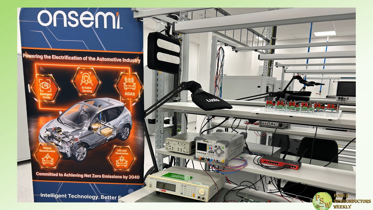
onsemi opened an application test lab in Piestany, Slovakia, focused on the advancement of system solutions for battery/plug-in hybrid/electric vehicles (xEVs) and energy infrastructure (EI) power conversion systems. The state-of-the-art systems applications lab provides specialized equipment to develop and test next-generation silicon (Si) and silicon carbide (SiC) semiconductor solutions in collaboration with automotive OEMs, Tier 1s and EI providers.
Modern semiconductor devices are essential for highly efficient power conversion in xEV powertrains and charging, as well as applications in renewable energy. The new lab will play a central role in ensuring that the development of future power products results in highly differentiated, value-add solutions tailored to customers’ specific requirements.
The new facility consists of two high-voltage power labs that focus on systems and device level development as well as evaluation of SiC/Si traction inverters and ACDC/DCDC power converters. Laser welding facilities, mechanical clean rooms and workshops further enable fast prototyping and testing of next-generation system solutions.
Evaluation capabilities for the next-generation system solutions include:
- Continuous 24/7 testing
- Internally developed and patented software and hardware solutions to support high-voltage power cycling via space vector modulation (SVM) and sinusoidal pulse width modulation (SPWM)
- High-accuracy logging devices for assessing SiC and Si health and reliability
- Simulation of the harsh conditions faced by inverters during operation, testing liquid-cooled devices at temperatures as low as minus 50 degrees C and up to 220 degrees C
- Wider range of industry-recognized software allows for the programing of FPGAs and ARM microcontrollers on site, as well as qualification testing, data analysis and 3D modeling
Original – onsemi
-
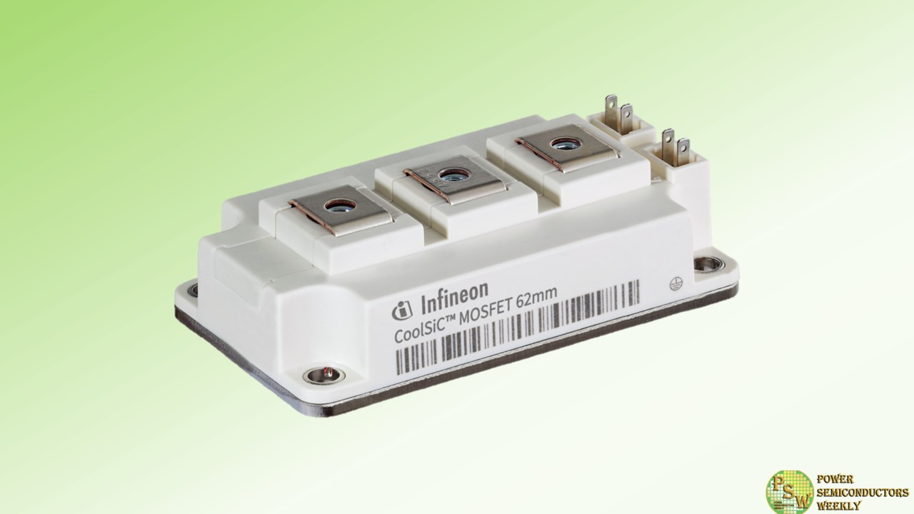
Infineon Technologies AG announced the expansion of its CoolSiC 1200 V and 2000 V MOSFET module families with a new industry-standard package. The proven 62mm device is designed in half-bridge topology and is based on the recently introduced and advanced M1H silicon carbide (SiC) MOSFET technology.
The package enables the use of SiC for mid-power applications from 250 kW – where silicon reaches the limits of power density with IGBT technology. Compared to a 62mm IGBT module, the list of applications now additionally includes solar, server, energy storage, EV charger, traction, commercial induction cooking and power conversion systems.
The M1H technology enables a significantly wider gate voltage window, ensuring high robustness to driver and layout-induced voltage spikes at the gate without any restrictions even at high switching frequencies. In addition to that, very low switching and transmission losses minimize cooling requirements.
Combined with a high reverse voltage, these devices meet another requirement of modern system design. By using Infineon’s CoolSiC chip technology, converter designs can be made more efficient, the nominal power per inverter can be increased and system costs can be reduced.
With baseplate and screw connections, the package features a very rugged mechanical design optimized for highest system availability, minimum service costs and downtime losses. Outstanding reliability is achieved through high thermal cycling capability and a continuous operating temperature (T vjop) of 150°C. The symmetrical internal package design provides identical switching conditions for the upper and lower switches. Optionally, the thermal performance of the module can be further enhanced with pre-applied thermal interface material (TIM).
The CoolSiC 62mm package MOSFETs are available in 1200 V variants of 5 mΩ/180 A, 2 mΩ/420 A and 1 mΩ/560 A. The 2000 V portfolio will include the 4 mΩ/300 A and 3 mΩ/400 A variants. The portfolio will be completed in Q1 2024 with the 1200 V/3 mΩ and 2000 V/5 mΩ variants.
An evaluation board is available for rapid characterization of the modules (double pulse/continuous operation). For ease of use, it provides flexible adjustment of the gate voltage and gate resistors. At the same time, it can be used as a reference design for driver boards for volume production.
Original – Infineon Technologies
-
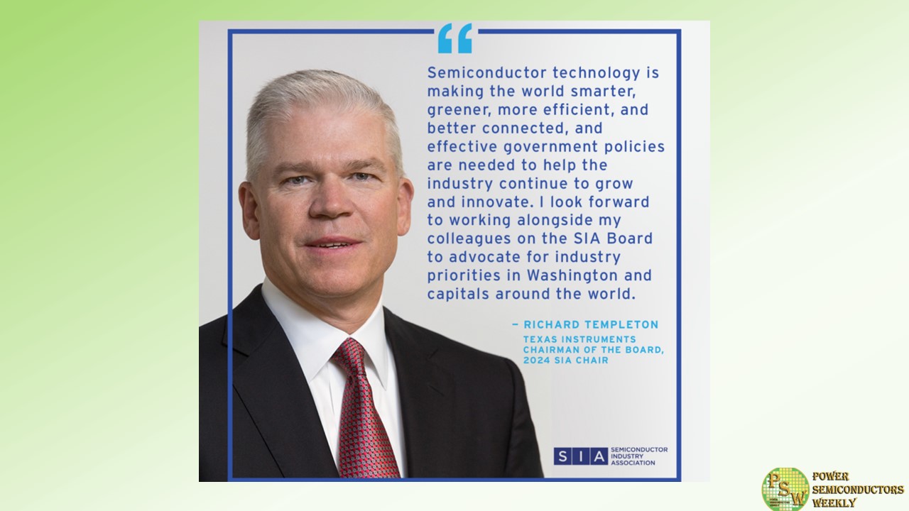
The Semiconductor Industry Association (SIA) announced Texas Instruments Chairman of the Board Rich Templeton has been elected Chair of the SIA Board of Directors and Western Digital CEO David Goeckeler has been elected SIA Vice Chair. SIA represents 99% of the U.S. semiconductor industry by revenue and nearly two-thirds of non-U.S. chip firms.
“It is a great pleasure to welcome our new leadership team for the year ahead, Rich Templeton of Texas Instruments and David Goeckeler of Western Digital,” said John Neuffer, SIA President and CEO. “Rich is extremely knowledgeable about the challenges we face as an industry and how we can overcome them, and David is a seasoned industry veteran and a highly effective champion for SIA’s priorities. Together, they will make an outstanding team as leaders of the SIA Board of Directors in 2024.
Templeton became Chairman of Texas Instruments in April 2008 and was President and CEO from May 2004 through March 2023. From April 2000 through April 2004, Templeton was Chief Operating Officer of TI. He was Executive Vice President of the company and President of TI’s semiconductor business from June 1996 through April 2004.
As CEO, Templeton maintained the company’s strategic investments in R&D and manufacturing, while expanding the size of the sales and applications engineering team to better serve TI customers. Under his leadership, TI emerged stronger, with better technological and product positions in both its core businesses. Templeton joined the company in 1980 after earning a B.S. in electrical engineering from Union College in New York.
“Semiconductor technology is making the world smarter, greener, more efficient, and better connected, and effective government policies are needed to help the industry continue to grow and innovate,” said Templeton. “I look forward to working alongside my colleagues on the SIA Board to advocate for industry priorities in Washington and capitals around the world.”
Since joining Western Digital in March 2020, Goeckeler has focused on the company’s transformation as the leading data storage producer in the industry. Before becoming CEO, he was Executive Vice President and General Manager of Cisco’s Networking and Security Business, with responsibility for more than $34 billion of the company’s global technology franchise.
He led a worldwide team of more than 25,000 engineers and oversaw Cisco’s networking and security strategy and market acceleration, including development operations for the company’s expansive technology portfolio and strategic acquisitions.
Original – Semiconductor Industry Association
-
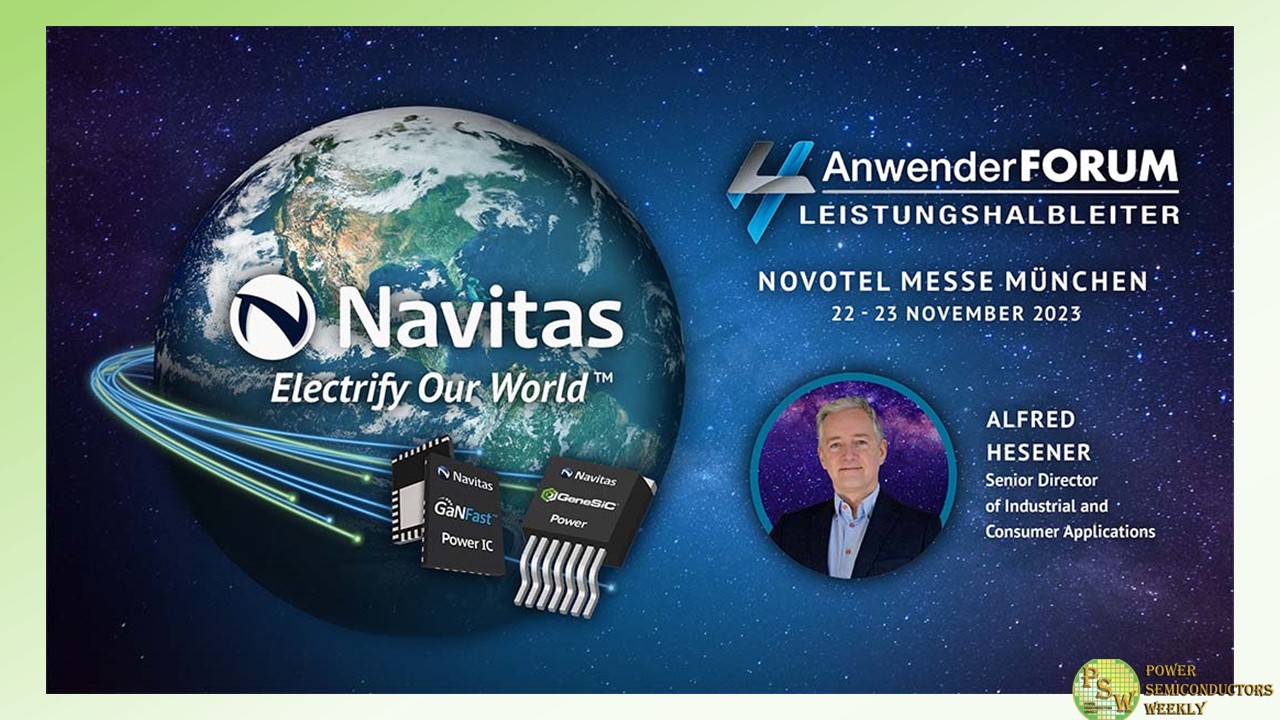
Navitas Semiconductor announced its participation in the Power Semiconductor User Forum, organized by WEKA Fachmedien on November 22nd -23rd, 2023. The event offers valuable insights into power electronics for developers and technical buyers.
Alfred Hesener, Senior Director of Industrial and Consumer Applications will explore “Reliability and Cost-of-Ownership Optimization in Industrial Power Supplies,” on November 23rd at 1:45 p.m. CET. Mr. Hesener will highlight next-generation solutions that achieve high power densities, cool operation, robust performance using Navitas’ GaNSense single and Half-Bridge power ICs.
Navitas’ GaNFast power ICs integrate GaN power and drive with control, sensing, and protection to enable faster charging, higher power density, greater energy savings and system cost reduction. In addition, each GaN power IC saves over 4 kg CO2 due to higher efficiency and dematerialization. New ‘Gen-3 Fast’ GeneSiC MOSFETs have up to 50% improved performance vs. other SiC devices, and save over 40 kg CO2 per unit vs. legacy silicon IGBTs.
“For industrial power designers, the WEKA forum highlights leading-edge, reliable technology for drives, pumps, chargers and power conversion, using GaN and SiC,” said Mr. Hesener. “Features like loss-less current sensing, programmable dV/dt, 2 kV ESD protection and autonomous sensing and protection are key enablers, and reduce time to market.”
WEKA Fachmedien’s Power Semiconductor User Forum 2023 will be held from November 22nd-23rd at the Novotel Messe Munich, Willy-Brandt-Platz 1, 81829 München, Germany.
Original – Navitas Semiconductor
