-
Abstract
The design and optimization of power converters is a key factor in the growth and development of the power electronics field. However, the process of designing a power converter is not straightforward, and engineers often rely on experience and intuition, sometimes requiring time-consuming computer simulations. This paper presents a tool for the basic design of grid-connected AC–DC converters. The design tool takes specifications and operating conditions for two-level and three-level NPC converter topologies and derives a draft design.
The tool calculates the input filter’s electrical parameters, the converter’s losses, the temperature rise of the power semiconductor devices, and the ripple current and voltage of the DC-link capacitor. In order to validate the proposed design tool, four AC–DC converters using SiC MOSFETs were designed. Based on the design results, simulation models and prototypes were fabricated to verify the performance and confirm that the proposed design tool can be used in the basic design process of converters.
1. Introduction
As the field of power electronics continues to evolve, the design and optimization of power converters is a key factor in the efficient conversion and utilization of energy. Power converters in various forms, such as AC–DC converters and DC–DC converters, play an important role in power management, motor control, and more in a variety of applications such as renewable energy systems, electric vehicles, industrial automation, and home appliances. The ability to design these power converters precisely and efficiently is crucial for meeting the energy efficiency, reliability, and sustainability requirements of the ever-evolving energy industry [1].
However, the process of designing a power converter is far from simple. There are complex tradeoffs between design features such as the power circuit structure, control scheme, and switching frequency and performance metrics such as efficiency, voltage ripple, and current ripple. Engineers designing power converters often rely on experience and intuition, and in some cases, complex computer simulations, to achieve optimal results. Even experienced professionals can find it difficult to design with new converter topologies, control schemes, etc., and it can take a lot of trial and error to learn how to do it, especially for newcomers to the field [2,3].
To solve this problem, studies have been conducted on procedures and methods for designing various types of power converters. References [4,5,6] present step-by-step procedures for designing power converters with specific converter topologies or introduce tools that can assist in the design. These works are mainly aimed at finding the optimal design point to achieve the targeted performance metrics when the basic design of the power converter is already completed. However, this approach can be difficult for someone not already familiar with the design of this type of converter.
Recently, methods using artificial intelligence (AI) have been studied to automate and reduce the reliance on experts in the converter and controller design phase [7,8,9,10]. These methods are well suited for use in the optimization design phase for specific target systems. However, AI-based design methods have the disadvantage of requiring simulations under various specifications and operating conditions to collect data, and the selection of appropriate training methods and the training process may require a considerable amount of resources.
Alternatively, basic power converter design tools are available, often provided by power semiconductor manufacturers [11,12]. However, the applicable converter topologies are limited, and device selection is also limited by the only components manufactured by the design tool vendor.
To address these issues, this paper introduces a general converter design tool for power converter design. The research project “Development of High Efficiency Power Converter based on Multidisciplinary Design and Optimization Platform”, funded by the Korea Institute of Energy Technology and Planning (KETEP), aims to build and operate an open web-based design tool for various power conversion systems based on wide-band-gap (WBG) semiconductors [13].
The design tool proposed in this paper is intended to be used in the basic design phase and is intended to quickly check feasibility or to quickly see how a particular performance varies as a function of parameter variation. The intention is to save the user of the design tool the effort of calculating formulas or building simulation models by hand. The tool is a synthesis of state-of-the-art research and practical engineering expertise and aims to simplify and popularize the process of power converter design and optimization. It provides engineers and researchers with an intuitive and user-friendly interface, allowing them to efficiently explore different design outcomes with a large number of degrees of freedom. It enables them to optimize the design parameters and ultimately deliver a high-performance solution for their specific needs.
These design tools can help accelerate the development of power conversion systems, foster innovation, and enable the rapid adoption of new technologies. Furthermore, they have the potential to popularize power conversion design knowledge. The popularization of this knowledge can play an important role in the development of new technologies and paving the way for a more sustainable and efficient future in power electronics.
This paper introduces a general power conversion design tool for grid-connected AC–DC converters as part of the general converter design tool. The design tool developed requires the ability to allow the user to select different types of components available on the market during the design process. For this purpose, it is difficult to use data that must be obtained through complex experiments, and it is possible to use only the level of information disclosed in the datasheets provided by the manufacturers of the devices. The proposed design tool also aims to have simple formulas and design procedures so that they can be used in a lightweight web-based design tool.
The proposed design tool primarily tackles the complexity inherent in power converter design. While traditional design methods heavily rely on complex computer simulations, the proposed tool simplifies this aspect, allowing for faster, more rapid, and more accessible design iterations. By making the design process more accessible and less dependent on deep expertise, the proposed tool helps to popularize power converter design knowledge, which is crucial for promoting innovation in the field.
In the next section, the procedure for the basic system design of an AC–DC converter is presented, and the formulas used in each design step are derived. Based on the proposed design procedure, the design of converters of various specifications was carried out, and simulation models and prototypes were produced based on the designed parameters to verify the results of the design tool.
2. Design Procedures
This paper presents a design tool for grid-connected three-phase AC–DC converters using SiC MOSFETs among various types of power conversion devices. The design tool aims to facilitate the drafting of designs by engineers with little experience in converter design. Figure 1 shows the design procedure. Viewing the converter as an electrical circuit composed of lumped elements, the basic specifications, such as the input and output voltages, capacity, and converter topology, are first selected. Limits are set on the efficiency, voltage and current ripple, and temperature rise of the semiconductors, and the switching devices are selected.
The input parameters include operating conditions such as the switching frequency and power factor, along with the previously selected items. Based on the input parameters, the tool calculates the ripple of the input current, the voltage and current ripple of the DC-link, derives the electrical parameters of the input filter and the DC-link capacitor, and calculates the converter loss and temperature rise to check whether the limit conditions are met.
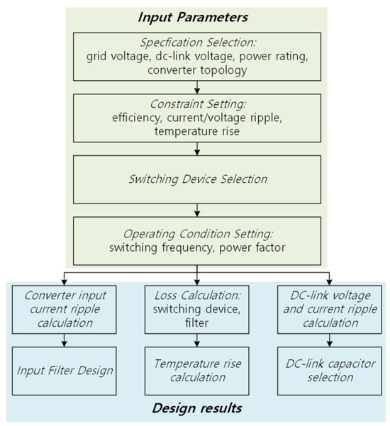
Figure 1. Grid-connected AC–DC converter design procedure.
However, this tool is intended for use in the basic design phase of a converter. In order for the web-based design tool to display design results quickly, the design procedure is based on simple formulas, and a certain amount of error is allowed. To develop a real product-level converter, more detailed design steps are required.
The component-level design of passive devices, such as inductors used in converters, component placement and mechanical structure design for power density optimization, and the electromagnetic field analysis and heat distribution analysis, which require finite element analysis, are not covered in this paper. The process and formulas used in the design tool are as follows.
2.1. Input Filter Design Procedure
In a grid-connected AC–DC converter, the purpose of the input filter is to reduce current harmonics at the input side caused by voltage harmonics generated by PWM switching. As an input filter circuit, a simple inductor or an LCL filter consisting of two inductors and one capacitor is commonly used. The design tool in this paper exploits an LCL filter that has high harmonic rejection performance per unit inductance.
Figure 2 shows the structure of the AC–DC converter and the LCL filter discussed in this paper. Lc and Lg represent the converter-side and grid-side inductors, respectively, and the filter capacitor, Cf, is connected in series with the damping resistor, Rd. The power stack is represented by a three-phase, two-level (2L) voltage-type inverter structure, which assumes the use of a three-phase, two-level or three-level (3L)-NPC converter in this paper.
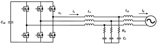
Figure 2. Grid-connected AC–DC converter structure with LCL filter.
Ignoring the effect of damping resistors in the converter structure of Figure 2, the relationship between voltage harmonics and current harmonics can be expressed as follows.

where ig is the grid-side current and vc is the output voltage at the converter side. The order-specific harmonics of the output voltage due to the switching of the converter can be calculated analytically [14]. With the limits of the target harmonic currents for each order, the input filter can be designed using the relationship in (1).
Table 1, Table 2 and Table 3 show the current harmonic limits by order of the current harmonic regulations IEEE-519 [15] and IEEE-1547 [16], which are widely used in designing grid-connected AC–DC converters. Studies on designing input filters have used the relationship in (1) to select input filter parameters that ensure that the voltage harmonics caused by the PWM of the converter do not exceed the current harmonic limits of each regulation [17,18].
Table 1. Current harmonic limits according to the IEEE 519 standard [15].
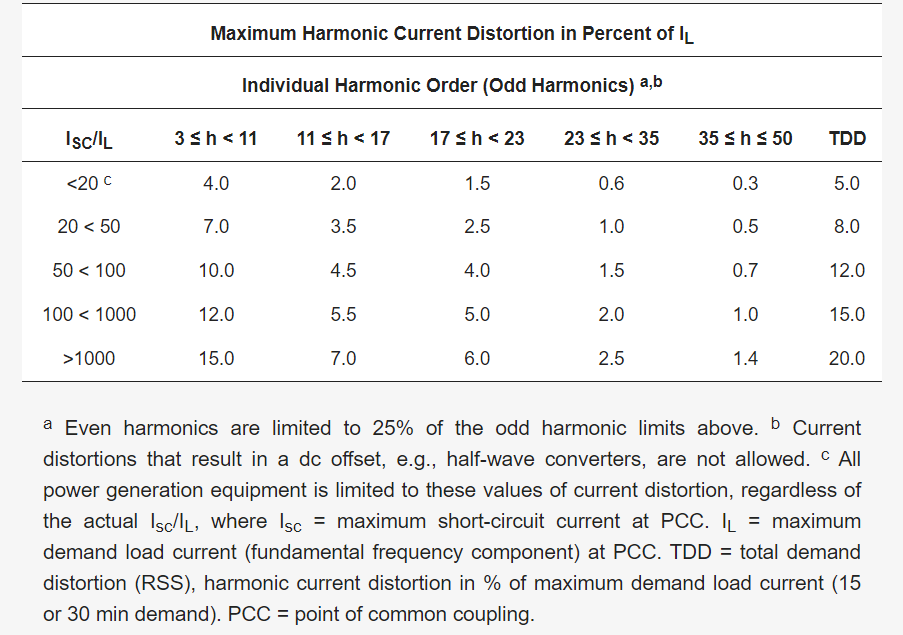
Table 2. Odd harmonic current distortion limit in percent of rated current (Irated) a according to IEEE 1547 [16].
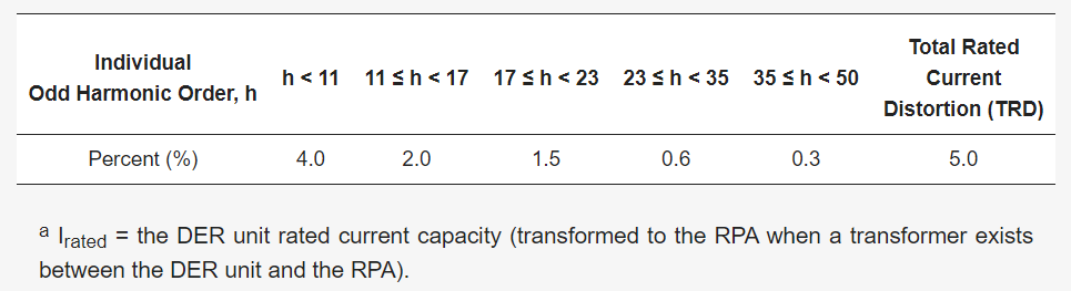
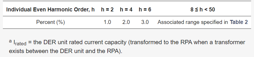
Table 3. Even harmonic current distortion limit in percent of rated current (Irated) a according to IEEE 1547 [16].
However, this approach may not be appropriate for converters using SiC MOSFETs. As shown by the relationship in (1), harmonics in the grid current are caused by harmonics in the output voltage due to the PWM operation of the converter. The output voltage harmonics can be roughly divided into two classes according to their order: higher-order harmonics around multiples of the PWM switching frequency and lower-order harmonics corresponding to multiples of the fundamental wave, such as the 5th, 7th, 11th, etc.
The higher-order voltage harmonics can be calculated analytically according to the PWM method by obtaining the magnitude of the harmonic voltage of each order, and filter parameters can be designed accordingly to limit the harmonic current of that order to a target value or less.
However, higher-order harmonics often account for a smaller proportion of the total current harmonic component generated by a grid-tied converter than lower-order harmonics. This is because higher-order harmonics have higher frequencies and are more easily attenuated by the input filters.
This is especially true for converters using SiC MOSFETs, which often have switching frequencies of tens of kHz or more. Furthermore, popular grid input current harmonic regulations, IEEE 519 [15] and IEEE 1547 [16], limit the harmonic frequency to no more than the 50th order of the fundamental wave. For converters using SiC MOSFETs, most have switching frequencies above 20 kHz, so the higher-order harmonics associated with the switching frequency are well beyond the 50th order when referenced to the typical grid frequency of 60 Hz, which is outside the harmonic regulation criteria.
When using input filters to satisfy grid current harmonics regulations, it is then necessary to design them with low-order current harmonics in mind, but it is difficult to accurately calculate the magnitude of the voltage harmonics that cause low-order current harmonics.
Low-order output voltage harmonics are due to the non-ideal output characteristics of the converter, such as dead time and a voltage drop across switching elements, and are difficult to obtain analytically. In addition, for converters using SiC MOSFETs with fast switching frequencies, harmonic current controllers can be used to significantly suppress low-order harmonics [17]. In practice, harmonic current controllers are often used, which can lead to overly large filter designs if their effects are not considered. However, the harmonic control performance of the controller is also difficult to accurately estimate at the filter design stage.
In this paper, an input filter design method based on limiting the maximum value of the ripple of the converter-side current below a certain value is used, rather than limiting the grid current harmonics below a certain value according to the regulations of [15,16], etc. The design procedure of the input filter is shown in Figure 3, and the detailed design process is as follows.
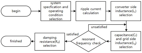
Figure 3. Inpul filter design procedure.
- Select system specifications and operating conditions. Select the grid voltage, grid frequency, converter type (2L or 3L-NPC), switching frequency, DC-link voltage, and rated current.
- Calculate ripple current and select converter side inductance. Set the converter-side ripple current limit. Select the limit value of the peak-to-peak amplitude of the current ripple relative to the rated current and calculate the converter-side inductor value that satisfies the ripple current according to the operating conditions. The peak-to-peak amplitude of the ripple current generated by the converter is determined by the operating conditions, and the instantaneous phase angle and can be expressed as (2) [18].

where Vdc is the DC-link voltage, Ts is the switching period, and r(m,θ) is a function of the voltage modulation index (m) and the output voltage phase angle (θ). The magnitude of the instantaneous current ripple depends on the phase angle, but the proposed method calculates the magnitude of the current ripple based on the output voltage at a phase angle of 90°.
In general, the power factor of a grid-connected converter is close to unity, so the output voltage and current are almost in-phase, and the magnitude of the current flowing in the converter is maximized around 90 degrees. Therefore, when considering the maximum current flowing through the converter due to current ripple, it is appropriate to base the design on the value when the phase angle is 90°. The converter-side inductance (Lc) value that satisfies the magnitude of the ripple current can be selected by using (2).
- Select capacitance and grid-side inductance. The larger the capacitor of the LCL filter, the better it can absorb the converter’s ripple current and reduce the harmonics of the grid-side current. However, the capacitor in the input filter introduces reactive power at the grid side and changes the grid side power factor. Typically, the reactive power flowing into the capacitor is limited to 2–5% of the apparent power in the design of the input filter [19]. The proposed design tool takes the reactive power value of the capacitor as input and selects the capacitor divisor of the corresponding filter. The formula for selecting the capacitance value is shown in (3).

where S is the apparent power of the converter, ω is the frequency of the grid, Vph is the phase voltage of the grid, and R is the ratio of the reactive power to the apparent power. In studies dealing with LCL filter design, the values of the grid-side inductance and the converter-side inductance are often chosen to be equal. This is because, when the resonant frequency of the LCL filter is first determined, equalizing the two inductance values results in the smallest magnitude of the total inductance [20], i.e., the harmonics of the grid current can be reduced the most with the same inductance value.
However, in this paper, the filter is designed based on the ripple current on the converter side, not the current harmonics delivered to the grid. In the case of converters using SiC MOSFETs, the low-order harmonics that contribute most to the grid current harmonics can be significantly suppressed by current controllers, so the proposed method focuses more on the converter-side inductor in the total inductance used in the input filter. In this paper, the grid-side inductance is selected as one-third of the converter-side inductance.
- Check the resonant frequency of the input filter. The resonant frequency (fres) of the input filter should be less than one-half of the sampling frequency (fs) according to the Nyquist sampling theory, and it should be higher than the bandwidth (fb) of the current controller to avoid affecting the current control behavior [21].

Finally, check whether the parameters of the input filter selected satisfies (4), and if not, adjust the capacitance value so that the resonant frequency satisfy the limitation of (4).
- Select damping resistor. The LCL filter theoretically has zero impedance at its resonant frequency. The damping resistor is used to provide impedance at this time to suppress the oscillation of the current at the resonant frequency. For this purpose, the value of the damping resistor is designed to be similar to the impedance of the capacitor connected in series at the resonant frequency [22], and in this paper, it is selected as one-third of the impedance of the capacitor at the resonant frequency.

2.2. Calculating Losses and Temperature Rise
The losses of the converter covered in this paper are composed of the losses of the power semiconductor and the losses of the input filter. The losses are calculated based on the given converter specifications and operating conditions, and the junction temperature is estimated using the thermal resistance information of the heat sink where the power semiconductor is installed.
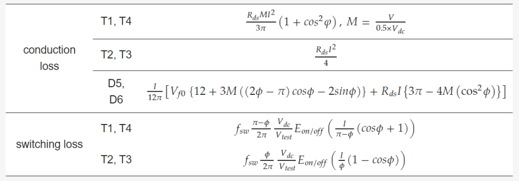
The losses of the power semiconductor can be divided into conduction losses and switching losses. The conduction losses of SiC MOSFETs and diodes are calculated using the Rds, Rd, and Vf0 information in the datasheet, as shown in (6) and (7), respectively, and the switching losses of SiC MOSFETs are calculated using the datasheet loss data, as expressed in (8).

where Rds is the equivalent resistance when the SiC MOSFET is turned on and Rd and Vfo are the equivalent resistance and threshold voltage when the diode is turned on, respectively. Irms is the rms value of the current flowing in each power semiconductor device, fsw is the switching frequency, s(θ) is duration when the current is flowing in that semiconductor device, Iavg is the average current in the current flowing section, Vdc is the DC-link voltage, Vtest is the test voltage indicated in the switching loss data in the datasheet, and Eon/off is the loss function extracted from the on and off switching loss data in the datasheet. The gate resistance is inputted by the user and reflected in the determination of Rds and Eon/off.
Equation (8) uses the average current in the conducting section to calculate the switching losses under the assumption that the current flowing in the device at the time of switching is proportional to the switching losses. In practice, the two are not exactly proportional. In general, for SiC MOSFETs, there is a slight exponential increase in switching losses as the current flowing through the device at the time of switching increases.
As a result, the switching losses calculated from the average current tend to be smaller than the actual switching losses at higher load currents, leading to calculation errors. However, since the design tool presented in this paper is intended to be used in the basic design phase for feasibility checks, this level of error can be justified. Overcurrent and overvoltage due to parasitic components like stray inductance also affect the switching loss [23]. However, the parasitic component cannot be anticipated during the basic design phase, so it is not reflected.
Figure 4 shows the leg structure of the two-level and three-level converters covered in this design tool, and the output voltage command and output current of the converter are shown in (9) and (10).

where V and I represent the magnitude of the output voltage command and output current, respectively, ω is the frequency of the grid, and φ is the load angle. In order to calculate the loss of each power semiconductor device, the operating region can be divided into four according to sign of output voltage command and output current.
Figure 5 shows the four operating areas with the state of the output voltage command and current. Table 4 summarizes the current-carrying devices and devices where switching losses occur in each operating area for 2L and 3L-NPC converters. Using Figure 5 and Table 4, it is possible to calculate the rms value of the current flowing through each power semiconductor element, the average current in the section where the current flows, and substitute the values into (6)–(8) to calculate the loss for each element in each converter, as shown in Table 5 and Table 6.
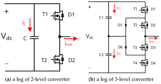
Figure 4. Leg configuration of AC–DC converters.
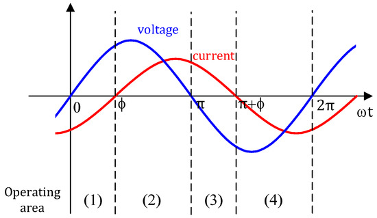
Figure 5. Operating area classification.
Table 4. Switch operation according to operating area.
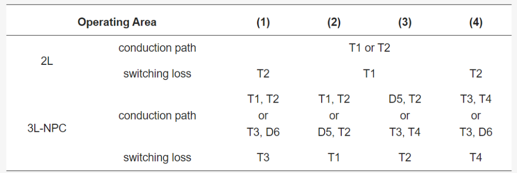
Table 5. Power semiconductor loss for 2L converter.

Table 6. Power semiconductor loss for 3L-NPC converter.
The calculated losses of the power semiconductor are used to calculate the junction temperature rise of the power semiconductor. Figure 6 shows the heat transfer circuit model used to calculate the temperature rise in this paper. The losses generated by the power semiconductor are denoted as Ploss, and the thermal resistance from the junction of the power semiconductor to the case, the thermal resistance from the case to the heat sink, and the thermal resistance from the heat sink to the atmosphere are denoted as Rth,jc, Rth,ch, and Rth,ha, respectively. Tjunction, Tcase, Theatsink, and Tamb represent the junction, case, heatsink, and ambient temperatures, respectively.
The heat capacity of each part is not considered, but only steady-state losses and thermal resistance are considered to calculate the junction temperature. Rth,jc and Rth,ch use the datasheet values of the semiconductor device, and Rth,ha of the heat sink can be entered to be used to calculate the temperature rise, as shown in (11).

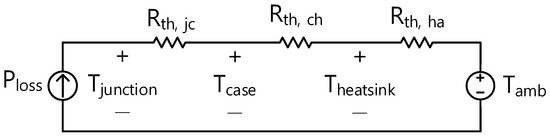
Figure 6. Heat transfer circuit.
More precisely, thermal resistance could be expressed as a function of temperature [24]. However, as shown in [24], for accurate modeling, the parameters should be obtained through testing for each component used in the converter, which is difficult to achieve with a basic design tool for various different types of components. The thermal resistance in this paper uses nominal values from the datasheet.
Most of the losses in the input filter come from the inductor. The loss of the inductor is determined by the design conditions, such as the core and winding used in the inductor, and the operating conditions, such as the magnitude and frequency of the voltage and current applied to the inductor. The conduction losses of an inductor are calculated using the resistance calculated from the cross-sectional area and length of the inductor windings, and the effective value of the current flowing in the inductor and the iron losses are calculated using the Steinmetz equation shown in (12) [25].

The coefficients required for the Steinmetz equation were obtained from the core’s datasheet information and added together by calculating the losses at the fundamental and switching frequencies. The flux density (B) was calculated using the magnitude of the fundamental wave current and the maximum ripple current magnitude, calculated using (2).
2.3. DC-Link Voltage, Current Ripple Calculations
The design tool in this paper derives the minimum DC-link capacitance values required during the converter design process. With the given system specifications and operating conditions, the DC-link capacitor currents of the 2L and 3L-NPC converters (iC of the 2L converter and iC1/iC2 of the 3L-NPC converter in Figure 4) can be calculated analytically, as shown in (13) and (14), respectively [26,27]. Table 7 shows the detailed formulas for the parameters used in (14).

Table 7. Expressions of A, B, C, and D in (14).
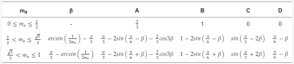
Taking the limit value of the voltage ripple as the input, the minimum value of the DC-link capacitor that satisfies the limit value can be selected as follows [26].

The tool selects the minimum value of the DC-link capacitor through equation (15) and derives the minimum value of the ripple current rating of the capacitor through (13) or (14).
3. Design Examples
Many cases of grid-connected AC–DC converters were designed using the converter design tool introduced in this paper. Table 8 shows the specifications and operating conditions of the design cases. All of them are 10 kVA-class grid-connected AC–DC converters and use 2L and 3L-NPC NPC converter topologies.
The grid to which they are connected is assumed to be typical three-phase 380 V 60 Hz converters. The current ripple ratio indicates the magnitude of the ripple current relative to the rated current. Cases 1 and 2 and cases 3 and 4 have identical specifications except for the current ripple specification, resulting in designs with different input filters.
Table 8. Specification and operating conditions for design cases.

Table 9 shows the minimum values of the input filter and DC-link capacitance derived from the design tool. In (2), the current ripple magnitude of the 2L converter is generally larger compared to the 3L-NPC converter, resulting in a larger inductance despite the higher current ripple limit of the 2L converter.
The minimum value of the DC-link capacitor resulting from the design is less than 10 μF, so in practice, the converter design should be based on selecting a capacitor that meets the current ripple rating. In such a design, the capacitance of the actual capacitor used is considerably larger than the minimum capacitance derived from the design tool, so that the voltage ripple caused by the current ripple is negligible.
Table 9. Input filter design results.

4. Simulation and Experimental Results
Based on the results of the design tool introduced in this paper, simulation models and prototypes were produced and compared with the design values. For the four cases of circuits in Table 8 and Table 9, simulation models were created using PSIM (version 9.0), and prototypes were fabricated and compared with the experimental results.
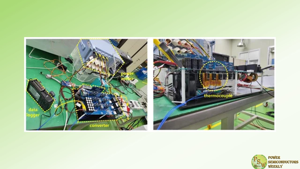
Figure 7 is a photo of the experimental set of one of the fabricated prototypes. The current ripple of the fabricated converter was measured using an oscilloscope, and the efficiency was measured using a power meter. The temperature rise was measured by attaching an NTC to the heatsink where the power semiconductor was installed.
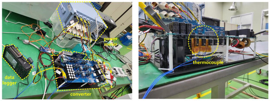
Figure 7. Experimental setup with prototype converter.
Figure 8 shows the waveforms of the fabricated simulation and the prototype. They represent the input line voltage, converter current, and grid current, respectively. It can be seen that the experimental waveforms have similar characteristics to the simulation results and behave appropriately.
Both the experimental and simulation results show that the ripple of the converter-side current varies with the circuit topology and the parameters of the input filters, but the harmonics of the grid-side current are not significantly different in all four cases. It can be seen that the low-order harmonics, which have a significant impact on the grid-side current quality, are sufficiently suppressed by the current controller.
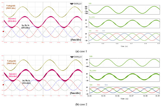
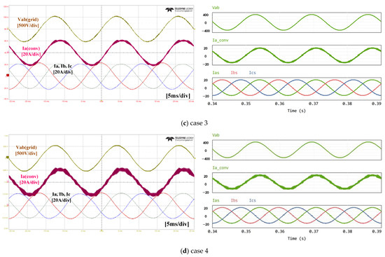
Figure 8. Experimental and simulation waveforms.
Table 10 shows the design values and experimental results of the current ripple, temperature rise, and THD of the grid current. For these metrics, only results at a rated load are compared, as their maximum values are considered during the design phase. The current ripple is similar to the design value for the 2L converter, while the 3L-NPC converter shows more deviation from the design value. In the 3L-NPC converter, the parasitic inductance along the switching path is larger due to the increase in the number of power semiconductor devices and the complexity of the busbar structure of the PCB, and the voltage spikes generated during switching have the effect of making the current ripple larger.
The THD of the grid-side current is not considered in the design tool introduced in this paper, but the measured current THD is shown to confirm that the input filter, considering only the converter-side ripple current, can keep the current THD low enough if a sufficiently good PR controller is used under a fast switching frequency. The temperature rise was calculated by measuring the temperature of the heatsink near where the power semiconductor is attached, as shown in Figure 7. In the model in Figure 6, the power semiconductor losses were calculated as Ploss and compared to Theatsink’s calculations and measurements.
The heatsink model was calculated with a simple concentrated integer thermal resistance, and the temperature of three heatsinks near the power semiconductor was measured and averaged. For the 2L converter, the temperature rise difference between the design and experimental results is smaller, but for the 3L-NPC converter, the deviation is relatively larger. In the case of the 2L converter, the number of semiconductor devices and the size of the heat sink are smaller, so the heat transfer structure is simpler and more in line with the simple model in Figure 6, but in the case of the 3L-NPC converter, the placement structure of the power semiconductor devices and the heatsink is relatively more complex, which is estimated to cause a slight deviation from the model.
Table 10. Current ripple, THD, and temperature rise of design value and experimental results.
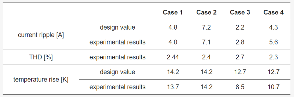
Figure 9 shows the calculated efficiency of the design tool and the measured efficiency from the experiment. The losses in the power semiconductor and the losses in the input filter were used to calculate the efficiency. Overall, the deviation between the measured and calculated efficiency at low loads is large, and the error decreases as the load factor increases.
At light loads, the iron losses in the input filter account for a large portion of the total losses, and it is assumed that the iron losses calculated through (12) are different from the actual losses incurred, leading to the error. The flux density is used as an input variable to calculate the iron loss in Equation (12). In the proposed design tool, the flux density is derived based on the maximum value of the current ripple calculated in (2).
However, in practice, the magnitude of the current ripple varies with the phase angle [28]. In the phase section where the current ripple is reduced, the flux density is also reduced, resulting in smaller iron losses. As a result, the calculated value of iron loss is larger than the actual value. Further improvements in flux density variation according to phase angle may be needed to increase the precision of the iron loss calculation. However, as a tool used in the basic design phase of a converter, it can be considered to have a reasonable calculation error. It is also appropriate that the calculation error is reduced under heavy loads, as efficiency at higher load factors is generally considered more important.
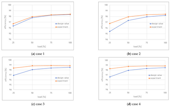
Figure 9. Efficiencies vs. loads of design value and experimental results.
5. Conclusions
This paper presents a design tool for designing three-phase grid-connected AC–DC converters. The basic design procedures for drafting the system design of a 2L or 3L-NPC converter were introduced, and the theory and formulas used in each design procedure were presented. The introduced design tools view the converter as an electrical circuit composed of lumped elements and set basic specifications, such as the input and output voltages, capacitance, converter topology, and limit conditions, such as the efficiency, voltage and current ripple, and temperature rise, and select switching elements.
Based on the input parameters, the ripple of the input current, DC-link voltage, and current ripple are calculated to derive the electrical parameters of the input filter and DC-link capacitor, and the converter losses and temperature rise are calculated to verify that the limit conditions are met.
The input filter uses the LCL filter structure, which is widely used in grid-connected converters. To limit the converter-side ripple current, the converter-side inductor value is determined first, and the grid-side inductor value is set accordingly. The capacitor value is determined according to the user-entered reactive power magnitude limit, and the damping resistor value is set to make the impedance of the input filter at the resonant frequency large enough.
Then, to calculate the efficiency, the converter losses are calculated. There are two main types of losses discussed in this paper: power semiconductor losses and input filter losses. The power semiconductor losses are calculated using the device’s datasheet information. The rms and average current flowing in each device are calculated and applied to the datasheet information of the power semiconductor device to calculate the conduction and switching losses.
The temperature rise is calculated using the thermal resistance information of the semiconductor device, the heatsink, and the previously calculated losses of the semiconductor device. The losses of the input filter are calculated by calculating the copper and iron losses of the inductor.
The current ripple in the DC stage is calculated analytically using the given system specifications and operating conditions. The calculated current ripple is used to find the minimum value of the DC-link capacitor that satisfies the voltage ripple given as a limit.
Using the introduced design tool, the converter design for various conditions is carried out and validated through a simulation and experiment. For four 10kVA-class converters, the design tool was used to derive the parameters of the input filter and the minimum value of the DC-link capacitor, and simulation models and prototypes were built based on the derived values and compared with the results of the design tool.
The experimental results showed that the temperature rise and current ripple magnitude were similar to the results of the design tool. The measured efficiency showed some deviation from the calculated value in the light-load region, but overall, the trend of efficiency change with load factor was similar in the design value and the experimental result, and the difference in the absolute values was small, showing that it is suitable as a basic design tool.
Authors
Original – MDPI
-
Abstract
This paper presents a high-speed level shifter with about 500 V/ns power supply slew immunity. In this designed structure, a narrow pulse-controlled current source is adapted to accelerate the voltage conversion and reduce the power consumption. A Fast-Slewing Circuit speeds up the operation of the level shifter based on the current comparison principle.
Edge detection technology is used to filter the generated voltage noise and achieve high dV/dt immunity. The proposed level shifter simulated with the 0.18 μm BCD (bipolar-CMOS-DMOS) process shows fast responses with a typical delay of 1.49 ns and 500 V/ns dV/dt immunity in the 200 V high-voltage application, which only occupies a 0.022 mm2 active area with the 0.18 μm BCD process.
1. Introduction
In recent years, the continuous growing markets in 5G communications, wireless transmission, fast charging industries, etc., create a huge demand for advancing today’s high-voltage (HV) power converters for cost and energy savings. Silicon-based power semiconductor devices have reached their physical limits due to their restrictions on device size and their physical characteristics. Although the switching losses in power devices can be reduced by applying technologies like soft switching, the large gate parasitic capacitance of silicon-based devices limits the optimization of energy loss, which affects the performance of power converters under high-input-voltage and high-frequency conditions [1].
Wide-bandgap (WBG) semiconductor materials, such as silicon carbide (SiC) and gallium nitride (GaN), have been demonstrated to offer excellent features compared to silicon. For instance, wide-bandgap (WBG) semiconductor materials allow smaller, faster, more reliable power electronic components than their silicon-based counterparts [2]. The wide-bandgap power devices exhibit greater thermal conductivity and electric field strengths, and as a result, SiC and GaN power devices have lower on-resistance to reduce conduction losses [3].
Therefore, the wide-bandgap GaN and SiC devices have gradually replaced the original silicon-based power semiconductor devices for their excellent performance advantages, producing a technological revolution in the fields of information communication, electric vehicles, and consumer electronics [4,5,6,7].
Usually, SiC and GaN power devices are used in half-bridge drivers as power switches. Level shifters are commonly employed as a transmission bridge between different voltage domains to shift the potential of the control logic from the low-voltage domain to the high-voltage domain or from the high-voltage domain to the low-voltage domain [8]. The high-voltage domain mainly includes level shift, high-side drive, and bootstrap circuits.
Unlike the supply voltage of the low-voltage domain (usually a fixed voltage below 5 V), the high-voltage domain is powered by floating power rails (VDDH and VSSH). When the high-side power transistor is turned on, the low-voltage VSSH of the floating power rail is approximately equal to the input voltage VHV of the half-bridge driver, and the high-voltage VDDH of the floating power rail is equal to VSSH + VCC.
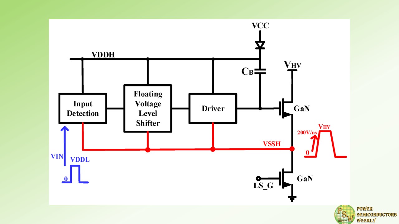
To turn on and off the high-side power transistor, the high-side driver needs to run on a floating power rail. The logic control signal is from the low-voltage domain and must be transformed to a high-voltage domain logic signal. As shown in Figure 1, the low-voltage control signal is sent to the level shifter after going via the Input Detection module, which activates or deactivates the high-side power transistor.
Therefore, as a bridge connecting the high-voltage domain and the low-voltage domain, the level shifter is one of the most critical circuits in the half-bridge driver. However, the GaN and SiC MOSFET can generate larger dV/dt and di/dt noise in the fast switching. For GaN MOSFET, the dV/dt could be up to above 200 V/ns [9]. This fast slewing is particularly problematic on the high side of the half-bridge driver, as shown in Figure 1.
Figure 1. The block diagram of the GaN high-voltage half-bridge driver.
Figure 2 shows the reliability issues with traditional GaN drivers. When the high-side power transistor is activated, the voltage of VSSH will be quickly raised to VHV, and the rising speed is >200 V/ns. This dVSSH/dt change is coupled to the level shifter through a bootstrap capacitor. Since the level shifter can perform voltage conversion between the low-voltage domain and the high-voltage domain, MH1 and MH2 are high-voltage transistors, whose parasitic capacitance is large.
The parasitic capacitance will generate a charging or discharging current when dV/dt happens, which will interfere with the level shifter’s normal operation and cause errors in the driver’s logic voltage of the high-voltage domain [10,11,12]. In Figure 2, it can be seen that under the action of the bootstrap capacitor CBOOT, VDDH changes with VSSH, and dVDDH/dt is approximately equal to dVSSH/dt. However, since the input MOS device MH1 of the level shifter is a high-voltage transistor, there is a large parasitic capacitance Cpar at node A.
The rapid change of the VDDH acts on Cpar to generate a large current, which pulls down the voltage of node A. When the noise amplitude (=R × Cpar × dVSSH/dt) generated at node A is larger than (VBOOT − VT), the recovery circuit of the subsequent stage may transmit the noise signal by mistake, where VBOOT is equal to VDDH − VSSH. Therefore, the dV/dt immunity capability of the driver is limited by the parasitic capacitance of the HV transistor of the level shifter.
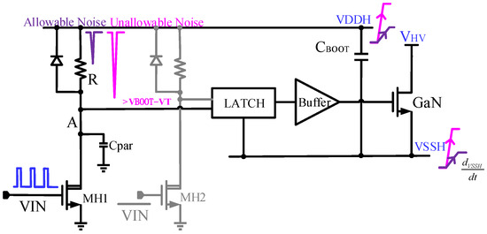
Figure 2. Reliability problem of the traditional level shifter.
Existing high-voltage level shifters have employed a number of design techniques to improve dV/dt immunity [13,14,15]. In [13], the author proposed a level shifter based on high-bandwidth current and latch structure; the delay is 370 ps, but the dV/dt slew immunity is only 30 V/ns. Yang et al. adopted a new technique to enhance the slew rate of level shifters, achieving a novel level shifter with 120 V/ns immunity and 20 ns propagation delay [14].
The level shifter (LS) proposed in [15] is designed with a current mirror/latch structure, and a common-mode noise canceller is also applied to enhance the dV/dt immunity. This level shifter achieves 200 V/ns noise immunity and sub-nanosecond delay in the SOI process, but this good performance is limited by the process. As the supply voltage increases, level shifters made with traditional processes suffer more from dV/dt noise. Then the ensuing problem is that the level shifter needs to consume more energy to enhance the dV/dt immunity of the circuit. As a result, several conventional structures designed to enhance the dV/dt noise immunity of the level shifters become inappropriate as the power supply voltage rises.
This paper presents a high-speed and high dV/dt immunity floating-voltage level shifter in the 0.18 μm BCD process. The proposed design can achieve a small propagation delay and an ultra-high dV/dt noise shielding function.
The rest of this paper is organized as follows: In Section 2, two conventional level shifter designs are reviewed. In Section 3, a novel enhanced level shifter is proposed, and its propagation delay and dV/dt immunity are analyzed in detail. Section 4 and Section 5, respectively, display the simulation results and conclusion.
2. Previous Level Shifter
A conventional level shifter is shown in Figure 3 [16]. The MOS transistors M1–M4 are high-voltage transistors. LDNMOS (laterally diffused N type metal oxide semiconductor) transistors M1 and M2 connect their gates to VDDL to protect and clamp the low-voltage (LV) transistors ML1 and ML2. In addition, the circuit connects the gates of the LDPMOS (laterally diffused P type metal oxide semiconductor) transistors M3 and M4 to VSSH to protect the low-voltage transistors ML5 and ML6 from being damaged by breakdown.
This circuit can convert the low-voltage power rail signal from GND-VDDL to the high-voltage floating power rail signal VSSH-VDDH. However, LDNMOS and LDPMOS transistors increase the parasitic capacitance and cause large propagation delays. More seriously, this structure suffers from mismatch delay and low dV/dt noise immunity. This level shifter has inconsistent low-to-high and high-to-low conduction delays due to the current asymmetry between the rising and falling edges of the output node.
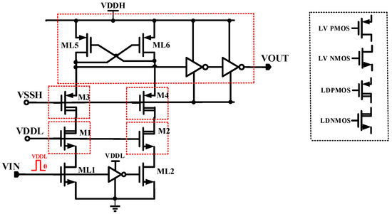
Figure 3. Traditional level shifter based on high-voltage PMOS clamping.
Figure 4 shows another type of conventional level shifter [17]. This topology clamps the voltage at nodes N1 and N2 to VDDH − VGS by using the diode-connected low-voltage PMOS transistors M1 and M4, where VGS is the gate-source voltage of the PMOS transistors. When the input signal VIN switches from low to high, the high-voltage tube LDNMOS1 is turned on; then the potential of the N1 point is pulled down, and the potential of the N2 point rises.
However, the potential at point N1 decreases more slowly than the potential at point N2 rises due to the current asymmetry. In the same way, when the VIN switches from high to low, the high-voltage tube LDNMOS2 is turned on; then the potential of the N2 point is pulled down, and the potential of the N1 point rises. The falling speed of the potential at point N2 is slower than the rising speed at point N1. For the structure in Figure 4, only a pair of high-voltage transistors, LDNMOS1 and LDNMOS2, are used, which has a lower parasitic capacitance than the structure in Figure 3. However, this level shifter faces the same difficulties as the structure shown in Figure 3, namely, that there is a severe mismatch delay and low dV/dt noise immunity.
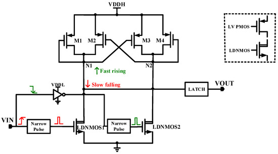
Figure 4. Traditional level shifter based on diode-connected PMOS clamping.
3. Proposed Enhanced Level Shifter
As shown Figure 5, this paper presents a high-speed and high dV/dt immunity level shifter which consists of three parts: the Power Supply Rail Conversion Circuit, the Fast-Slewing Circuit (FSC), and the dV/dt Noise Shielding Circuit. The Power Supply Rail Conversion Circuit converts the signal from the low-voltage domain to the high-voltage domain. The Fast-Slewing Circuit speeds up the level shifter’s signal conversion. And then the dV/dt Noise Shielding Circuit can shield the dV/dt noise to make the output of the level shifter remain constant.
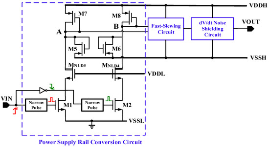
Figure 5. Top structure and strategy of the proposed level shifter.
In Figure 5, the input transistors M1 and M2 are low-voltage MOS devices. The diode-connected transistors M7 and M8 are used to clamp the voltages of node A and node B. The gate of the high-voltage transistors MNLD3 and MNLD4 are connected to the low-voltage rail power supply VDDL to bear high voltage, preventing the breakdown of the low-voltage transistors M1 and M2. The M5 and M6 transistors are used in the form of diodes, with their sources connected to the floating power supply ground VSSH to ensure that the voltages of node A and node B can be higher than VSSH − VTH (VTH is the threshold voltage of the MOSFET).
This prevents the drain-source voltage of the M7 and M8 devices from exceeding the safe voltage range. A narrow pulse generation circuit is adopted to generate the instantaneous driving signal and speed up the operation of the level shifter [18]. Additionally, the Fast-Slewing Circuit that was added to the circuit can speed up the voltage conversion rate of the level shifter even more, eliminating the issue of various mismatch delays.
The problem of dV/dt immunity is the most important concern of the level shifter, which can be analyzed from the two situations of positive swing and negative swing of the power supply. As shown in Figure 6, when the VIN is high, the normal states of VA − VSSH and VB − VSSH are low voltage and high voltage, respectively. When VSSH and VDDH quickly transition from high voltage to low voltage, both VA − VSSH and VB − VSSH rise to high voltage.
When VSSH and VDDH transition from low voltage to high voltage, both VA − VSSH and VB − VSSH can drop to low voltage. Therefore, the dV/dt Noise Shielding Circuit is meant to maintain the level shifter’s output in order to avoid the succeeding stage circuit from receiving the erroneous signal output of the level shifter.
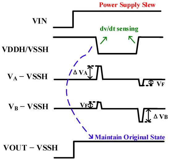
Figure 6. Noise shielding feature for dV/dt when the VIN is high.
3.1. Strategy for the Enhanced Level Shifter
The level shifter proposed in this article is shown in Figure 7. The signal conversion of the level shifter can be sped up by using the Fast-Slewing Circuit and the double-pulse generation circuit. The double-pulse generation circuit can generate a voltage pulse on the rising and falling edges of an input signal, consisting of a NAND gate, a capacitor, and several inverters. In the proposed level shifter, the input of this double-pulse generation circuit is the signal of the VIN, and the output of the circuit is used to control the on and off of M1 and M2.
Therefore, whenever there is a conversion of high voltage to low voltage or low voltage to high voltage, a large current will appear in the voltage conversion branch, improving the voltage conversion speed. At the same time, the transistors M1 and M2 are turned off during the voltage holding stage, so that the level shifter has very low static power consumption.
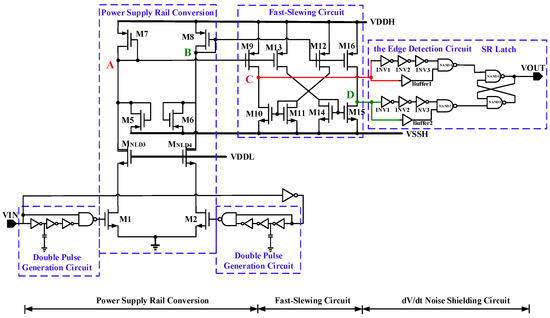
Figure 7. Schematic of the proposed level shifter circuit.
The Fast-Slewing Circuit is a current mirror that makes use of the principle of current comparison to achieve rapid voltage conversion speed [19]. As can be seen in Figure 7, when the VIN signal transitions from low voltage to high voltage, the voltage of node A can drop rapidly with the help of the huge pull-down capability of the transistor M1, while the asymmetric current of the circuit causes the voltage of node B to rise slowly.
Therefore, the proposed level shifter adopts the Fast-Slewing Circuit to improve the response speed. The voltages at nodes A and B are mirrored to nodes D and C through a current mirror, respectively, after passing through the Fast-Slewing Circuit, preventing the circuit from various mismatch delays. Then, the rising edge of node C or D can be captured by the edge detection circuit and locked by the SR latch, which finally changes the output of the level shifter and keeps it constant until the VIN changes.
3.2. The Propagation Delay of the Proposed Level Shifter
The proposed level shifter’s operation for switching from low to high is shown in Figure 8a. Before the VIN becomes high, VA is equal to VDDH, and VB is equal to VSSH. The signal transmission process of the level shifter is as follows:
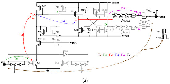
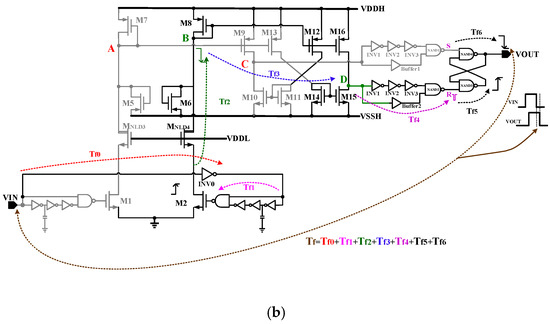
Figure 8. The suggested level shifter’s switching operation: (a) low-to-high switching operation; (b) high-to-low switching operation.(1)
When the VIN changes from low voltage to high voltage, the generation circuit, which consists of a NAND gate, a capacitor, and several inverters, generates a voltage pulse on the rising edges of the VIN signal. The delay in this process is called Tr0, which is determined by the delay of the NAND gate.(2)
When the voltage pulse generates, the input transistor M1 is turned on, and the voltage VA at node A begins to drop rapidly. The delay in this process is called Tr1. The strong pull-down capability of M1 will briefly provide a large current to the branch where node A is located to increase the response speed of node A.(3)
The current M7 is mirrored by the M9. Due to the small current of M10, the current of M9 is much greater than that of M10, so the potential at node C is rapidly raised to VDDH. The Tr2 is the transmission delay from node A to node C, which is determined by the delay of the current comparator.(4)
The edge detection circuit can identify the rising edge signal of node C. When VC becomes high, a short pulse signal is generated at node S under the action of the delay chain composed of INV1-INV3 and NAND1. Tr3 is the delay of the edge detection circuit.(5)
The generation of a short pulse signal VS triggers the flipping voltage of NAND4. At this point, the VOUT transitions from low to high and remains at VDDH until a short pulse occurs at node R. The delay between VS and VOUT is described by Tr4, which is the delay of NAND4.
The current of M7 can also be mirrored to M15 through M13 and M14. Due to the small current of M16, the voltage at node D is quickly pulled down. Although the descent speed of VD is slower than the ascent speed of VA, the drop of VD is not detected by the edge detection circuit and is just prepared for the next reset. Therefore, when the input signal VIN changes from low to high, the speed at which the voltage at node D changes has no effect on the circuit.
As shown in Figure 8b, when the input voltage of the level shifter transitions from high to low, the propagation delay Td_f of the signal consists ofTf0, Tf1, Tf2, Tf3, Tf4, Tf5, and Tf6. Due to the good symmetry of the proposed level shifter, Tr0 is equal to Tf1, Tr1 is equal to Tf2, Tr2 is equal to Tf3, Tr3 is equal to Tf4, and Tr4 is equal to Tf5. Therefore, it can be seen that Td_f has two more delay items, Tf0 and Tf6, than Td_r, which are the delays of the two NAND gates. Therefore, Td_r is smaller than Td_f.
3.3. The dV/dt Immunity of the Proposed Level Shifter
The edge generation circuit of the proposed level shifter has two functions. One is that the edge generation circuit can output a pulse signal at the rising edge and falling edge of the input signal; on the other hand, the edge generation circuit generates a large current during the narrow pulse signal to help the signal transfer quickly, and reduces the overall power consumption of the circuit by turning off the input transistors M1 and M2 during the VIN signal hold.
The transient operation of the proposed level shifter is demonstrated with low-to-high and high-to-low operations. When the VIN shifts from low to high, M1 is activated and M2 is turned off. The voltage at node A starts declining, the dropping edge of node A is sampled, and the rise of node C is accelerated by the current comparison circuit. The rising edge of node C is delayed by the delay circuit composed of the inverters INV1–INV3, and then the delayed signal is input to NAND1 together with the signal of node C. Next, a low-voltage pulse signal S is generated, and then the voltage of the VOUT changes from low to high.
When the input signal VIN changes from high to low, M2 is turned on, and M1 is turned off. The voltage at node B begins to drop, and then the falling edge of node B is sampled, which speeds up the rising speed of node D. The rising edge of node D can be delayed by the inverters INV4–INV6 and this delayed waveform is input into NAND2 with node D. At this time, a low-level pulse is generated in R to make the VOUT change from high to low. Figure 9 shows the waveform of the level shifter during the VIN transient changes.
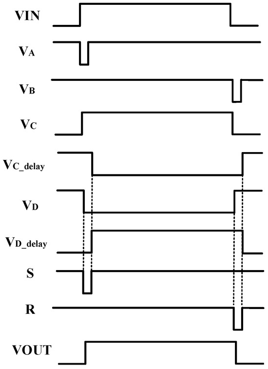
Figure 9. The waveform of the level shifter during VIN transient changes.
The proposed level shifter can shield dV/dt noise by using the dV/dt Noise Shielding Circuit, which consists of INV1–INV6 and NAND1, NAND2. The voltages at nodes C and D will rise or fall synchronously when dV/dt noise is generated due to rapid changes in the VSSH and VDDH. If the dV/dt noise is high, voltage changes at nodes C and D may trigger the logic gates of the edge detection circuit. Positive dV/dt noise will cause undershoot voltage at nodes C and D, and negative dV/dt noise will cause overshoot at nodes C and D.
However, these generated voltage noises will be filtered after passing through the edge detection circuit, so that no error signals will be generated at the S and R terminals, and the state of the RS latch will not be changed. Therefore, the proposed level shifter can shield the dV/dt noise from disturbing the output VOUT, so that the VOUT can remain constant.
4. Simulation Results
The proposed level shifter is simulated at the 0.18 μm BCD process using the Cadence Virtuoso tool. Figure 10 shows the simulated propagation performance of the proposed level shifter with 205 V VDDH and 200 V VSSH under the typical process corner. All power rails are supplied with fixed voltage sources during simulation (VDDH − VSSH = 5 V, VDDL = 5 V). The VIN is operated under 5 V supply voltage, and the low voltage of the VOUT is 200 V and the high voltage is 205 V.
It can be seen from Figure 10 that when the rising edge of the VIN is generated, the voltage at node A drops and triggers the low-voltage pulse signal of the S terminal of the RS flip-flop, and then the VOUT starts to flip from low to high. The voltage at node B decreases when the falling edge of the VIN arrives; then the R terminal of the RS flip-flop generates a low-voltage pulse signal, and the VOUT starts to change from high to low. The simulation results show that the propagation delay of the rising edge is about 1.23 ns, and the propagation delay of the falling edge is about 1.75 ns.
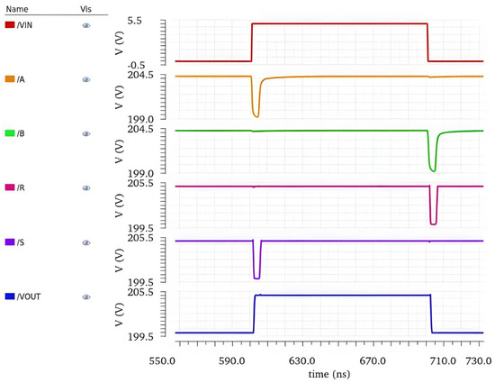
Figure 10. Propagation delay of the proposed level shifter.
Figure 11a,b show the rising and falling delays of the proposed level shifter under three process corners, ss (Worst Case), tt (Typical Case), and ff (Best Case), at temperatures −55 °C and 150 °C. The simulation results show that the minimum rising delay is 479 ps and the maximum is 2.64 ns; the minimum falling delay is 842.1 ps and the maximum is 3.4 ns.
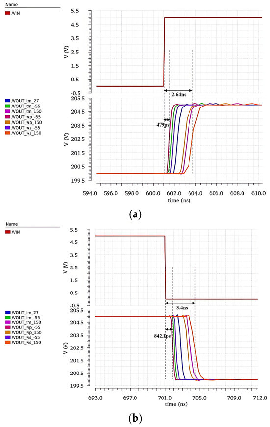
Figure 11. Simulation results of the proposed level shifter’s delay: (a) rising delay; (b) falling delay.
Figure 12 simulates the dV/dt noise shielding function of the proposed level shifter at ±500 V/ns dV/dt noise. The simulation results show that when dV/dt noise is generated, the voltages VS and VR have no erroneous logic signals during the period when the input signal VIN is high, the output signal VOUT is not disturbed by dV/dt noise, and the state remains unchanged.
Therefore, this can demonstrate that the level shifter proposed in this paper can achieve ±500 V/ns dV/dt immunity, which is also suitable for other supply voltages and processes. Figure 13 shows the layout of the proposed level shifter. The chip area is only 127 μm × 178 μm at the 0.18 μm BCD process.
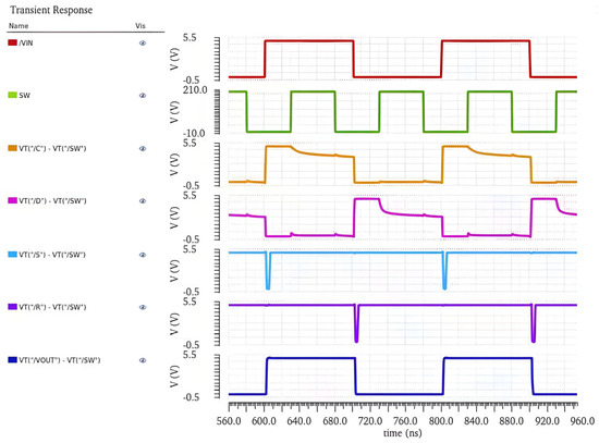
Figure 12. Simulation results of the dV/dt noise shielding function of the proposed level shifter.
Figure 13. The layout of the proposed level shifter.
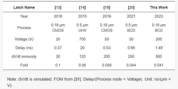
Table 1 shows the performance comparison between the proposed level shifter and previous reported level shifters. FOM is used to evaluate the performance of the level shifter by combining delay, supply voltage, and process node. It can be seen from Table 1 that the high-voltage level shifter proposed in this paper has the highest dV/dt immunity and the smallest FOM. Therefore, the proposed level shifter can still achieve sufficient response speed and high reliability under a 200 V power supply.
Table 1. Comparison with previous work.
5. Conclusions
This paper presents a high-voltage level shifter for a GaN half-bridge driver that offers high-speed operation and high dV/dt immunity. A narrow pulse-controlled current source and the Fast-Slewing Circuit speed up the transmission of the level shifter and reduce the power consumption. Edge detection technology is utilized to filter the generated voltage noise and then achieve the ultra-high dV/dt immunity of the level shifter without using complex auxiliary circuits.
In the 0.18 μm BCD process, the proposed level shifter can achieve a propagation delay of 1.49 ns and a 500 V/ns dV/dt immunity under a 200 V power supply, which only occupies a 0.022 mm2 active area. The FOM is very small, which is only 0.041. The suggested level shifter can be utilized in multi-MHz converters because of its low propagation delay and its ability to provide 500 V/ns of slewing immunity, making it suitable for drivers of wide-bandgap power device applications.
Authors
Min Guo, Lixin Wang, Shixin Wang, Yuan Zhao and Bowang Li
Original – MDPI
-
Abstract
This paper investigates and compares the static performance and short-circuit (SC) robustness of 1200 V SiC MOSFETs with varying JFET widths (WJFET = 2.0–5.0 μm). Short-circuit measurements as well as electrical-thermal simulations are used to identify thermal distribution and maximum electrical field, providing valuable insights into the design limits. The devices under test (DUTs) with narrow and wide WJFET exhibit different failure mechanisms under SC stress.
After the short-circuit failure, interlayer dielectric (ILD) cracks are observed in DUTs with narrow JFET width (WJFET < 3 μm). In contrast, it is discovered that the burn mark is located in the channel region of the device with a wide JFET width. Moreover, the short-circuit withstand time (SCWT) of DUTs with narrow and wide WJFET exhibits varying trends under high temperature conditions (100 °C). These results can help verify the different failure mechanisms and determine an optimal JFET design to improve the trade-off between the static performance and SC ruggedness of the SiC MOSFETs.
1. Introduction
SiC MOSFETs have already emerged as one of the most crucial components in power electronic systems. They can be utilized at frequencies exceeding 100 kHz, which can facilitate a reduction in the volume of passive components and enhance the power density of the system [1]. MOSFETs are gaining increasing popularity in electric vehicles (EVs), hybrid electric vehicles (HEVs), and railways, with a growing interest in their reliability and robustness.
Approximately 38% of inverter failures can be attributed to the failure of power devices induced by short-circuit (SC) stresses [2,3,4]. During the device operation, unexpected circuit faults may occur. For example, in the half-bridge circuit, failures often arise from short circuits in the upper or lower bridge devices, and the device channel may accidentally conduct current when the device withstands the high drain voltage. This high current density flowing through the device can lead to device failure.
Numerous investigations have been conducted on the short-circuit characteristics of commercial SiC MOSFETs. The results of the short-circuit test provide valuable information about the SiC MOSFET’s ability to handle short-circuit faults without suffering permanent damage. It helps in determining the device’s short-circuit withstand capability, evaluating the effectiveness of its protection mechanisms, and assessing its thermal management strategies [5].
This knowledge is crucial for designing reliable power electronic systems that utilize SiC MOSFETs and ensuring their safe operation under various fault conditions. The short-circuit performance of SiC MOSFET power modules under various operating conditions has also been studied [6,7]. Compared to Si IGBTs, the short-circuit withstand time (SCWT) of SiC MOSFETs is 80% shorter due to their larger current densities and higher electrical fields [7]. During the short-circuit (SC) process, the heat generated in SiC MOSFETs leads to a rapid increase in the junction temperature, exceeding 1000 °C [8,9].
The rapid increase in junction temperature induces thermal and mechanical stress on the interface between aluminum and the interlayer dielectric. This stress has been observed to cause cracks at the corner of the interlayer dielectric, as reported in references [10,11]. The oxide thickness, Pwell doping and channel length have been extensively studied in SiC MOSFETs [12,13,14]. Channel structure on the short-circuit capability of SiC MOSFETs has been investigated. The impacts of channel design parameters, such as doping profiles and dimensions, are compared, offering guidelines for optimizing the channel structure for enhanced short-circuit performance [15].
The impacts of gate structure on the short-circuit performance of SiC MOSFETs are explored. Different gate designs influence the device’s ability to handle short-circuit events, providing insights into optimizing the gate structure for improved short-circuit withstand time [16]. However, the short-circuit robustness of SiC MOSFET with different JFET widths and the optimal design for JFET width are still under investigation. JFET width is the vital parameter in SiC MOSFET, which not only affects the on-resistance, electrical field at oxide, but also influences the saturate current and short-circuit characteristics.
The device researcher always focuses on the optimal parameters in static performance, but the comparison of short-circuit characteristics of switches with different JFET widths needs to be evaluated. Furthermore, devices from various manufacturers have different value (Commercial device of A company has the width of 1.75 μm. Commercial device of B company has the width of 2.8 μm).
In this study, SiC MOSFETs with various structural parameters are fabricated and their impacts on short-circuit capability are investigated. The correlation between short-circuit withstanding time and measurement temperature is studied. Electrical-thermal simulations are used to identify thermal distribution and maximum electrical field, providing valuable insights into the design limits. Additionally, device failure mechanisms are analyzed based on experimental and simulation results for different structure designs. Finally, the optimal structure design of SiC MOSFETs is summarized for improving the trade-off relationship between device conduction performance and short-circuit ruggedness.
2. Materials and Methods
2.1. Static Characteristics of SiC MOSFETs with Different Structural Parameters
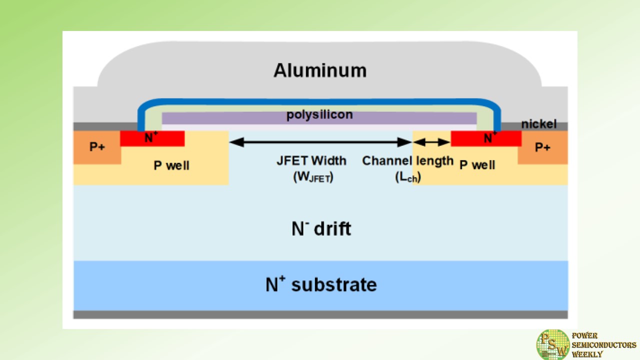
As shown in Figure 1, the JFET width (WJFET) is one of the key structural parameters for SiC MOSFETs, which significantly affects both device performance and reliability. To study its impact on short-circuit ruggedness, 1200 V SiC MOSFETs with various WJFET (2.0, 2.5, 3.0, 4.0, and 5.0 μm) are fabricated in this work. In the fabricated SiC MOSFETs, the channel doping is 1 × 1017 cm−3, the drift region doping is 8 × 1015 cm−3 and the drift thickness is 12 μm. The fabrication flow is shown in Figure 2. In SiC MOSFET, the JFET region is located between two adjacent P well regions.
And P well—Nepi—P well is like JFET (junction field effect transistor), so this region is named the JFET region. Due to the intrinsic depletion region, the real current path is narrower than the dimension of WJFET. To optimize, the minimal resistance and minimize electrical field are at the center of gate oxide (<3 MV/cm).
Figure 1. The schematic diagram of the 1200 V SiC MOSFET.
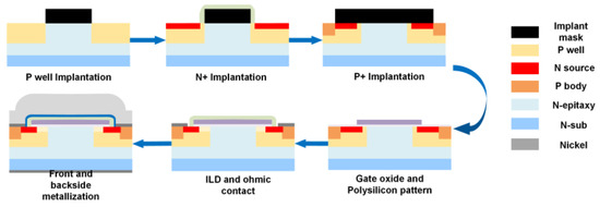
Figure 2. Manufacture flow of the 1200 V SiC MOSFET.
The five SiC MOSFET devices in this study are labeled A1–A5. The devices have identical active areas and chip sizes. In this section, the static characteristics of the five MOSFET devices are measured and analyzed.
The transfer, output and blocking I–V (current-voltage) characteristics of the five devices are measured by Keysight B1505A equipment and the results are compared in Figure 3. For the transfer I–V characteristics, the drain-source voltage (VDS) is set to 10 V in the measurement. For the output I–V characteristics, the gate-source voltage (VGS) is set to 20 V. For the blocking I–V characteristics, the VGS is set to 0 V. Device performance indexes, such as threshold voltage, resistance, transconductance and breakdown voltage are extracted and summarized in Table 1.
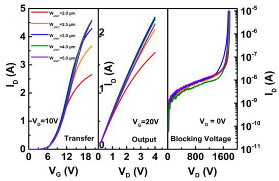
Figure 3. Static characteristics of SiC MOSFETs with different JFET widths.
Table 1. Static characteristics of SiC MOSFETs with different JFET widths.
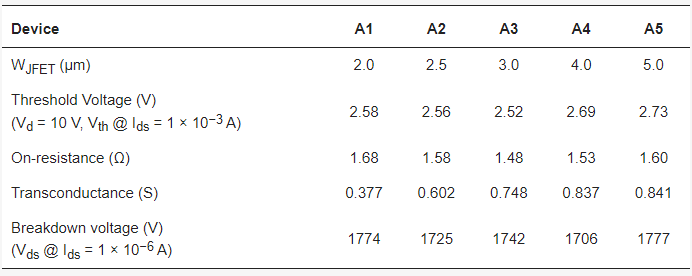
With increasing WJFET design, the threshold voltage initially decreases from 2.58 to 2.52 V, and then increases to 2.73 V. Correspondingly, the on-resistance decreases from 1.68 to 1.48 Ω, and then increases to 1.6 Ω. The transconductance of the device gradually increases from 0.377 to 0.841 S. Besides, from the blocking characteristics, all five devices can successfully achieve blocking voltages above 1700 V.
The on-resistance of a SiC MOSFET device is composed of channel resistance, JFET region resistance, drift layer resistance and substrate resistance. For 1200 V SiC MOSFETs, JFET region resistance contributes around 30% of the total resistance at room temperature. Increasing the WJFET can help reduce the JFET region resistance. However, it can also result in an increase in the cell pitch and a decrease in channel density, if the source region width remains constant. According to the experimental results, Device A3 with WJFET = 3 μm achieves the lowest resistance of 1.48 Ω among the five designs.
The output characteristics of the five devices are measured at 25 to 175 °C to investigate the conduction performance of SiC MOSFETs at high temperatures. The on-resistances at different temperatures are presented in Figure 4. It can be observed that the on-resistance increases with temperature for all five devices, but the temperature coefficient of resistance varies for different WJFET designs.
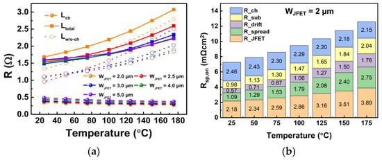
Figure 4. (a) Compositional channel resistance and total resistance at elevated temperature. (b) Compositional resistance in Device A1.
The channel resistance of VDMOS is determined by calculating the resistance of lateral long channel MOSFET and converting it based on channel length and width, as seen in Figure 4. The channel resistance accounts for more than 30% of the total resistance. The channel resistance decreases as the temperature increases from room temperature to 175 °C. At higher temperatures, the threshold voltage of the device decreases, resulting in an increased generation of electrons in the channel. Furthermore, higher electron densities in the channel provide a better screening effect, reducing the Coulomb scattering caused by interface traps.
These two factors contribute to the overall reduction in channel resistance [12]. Apart from the channel resistance, the bulk resistance exhibits a positive temperature coefficient, which is due to the lower mobility of carries at elevated temperatures caused by acoustic scattering. The opposite temperature behaviors of the channel resistance and bulk resistance components lead to the different trends in total resistance at elevated temperatures for devices with different WJFET. With a narrower JFET width, the JFET resistance becomes a larger proportion of the total resistance. Consequently, the total resistance increases more rapidly at elevated temperatures.
For Device A1, with a narrow WJFET design (2.0 μm), the JFET region resistance contributes significantly to the total on-resistance. It also has a positive temperature coefficient, resulting in the highest slope among the five devices in Figure 3. For Device A5, with a wide WJFET design (5.0 μm), the JFET region resistance contributes only a small portion to the total on-resistance. In contrast, the channel resistance plays a more significant role in determining the overall resistance of Device A5.
The negative temperature coefficient of the channel resistance in Device A5 counterbalances the positive temperature coefficient of JFET region resistance, drift layer resistance and substrate resistance. Thus, the slope of the curve for Device A5 in Figure 3 is the lowest among the five devices. For Device A3 to A5, the on-resistances are less sensitive to ambient temperature, which is good for high temperature applications. The slight increase in on-resistance with temperature is beneficial for balancing current in parallel connections.
The devices’resistance types are channel resistance, JFET resistance, drift resistance and substrate resistance, as shown in Figure 4, and the resistance is mainly based. To illustrate the reason for the transconductance and on-resistance exhibiting different trends, the different compositional resistance needs to be separated, as shown in Figure 4b. Transconductance is mainly controlled by channel resistance, as the channel resistance is dependent on the gate voltage. If the channel resistance occupies a larger portion in the on-resistance, the transconductance is higher. In five types of DUTs, the wider WJFET has a larger portion of channel resistance, so the transconductance is higher.
WJFET influence the cell pitch and also have a large impact on JFET resistance. When WJFET decreases, smaller cell pith results in the reduced channel resistance. However, narrower WJFET leads to increased JFET resistance, which is a trade-off in different devices. Among five types of devices, the WJFET = 3 μm is the optimal value.
2.2. Short-Circuit Capability of SiC MOSFETs
A short-circuit (SC) test platform has been established. Figure 5a illustrates the test bench, while Figure 5b presents the schematic diagram of the test board. The device under test (DUT) is connected in series with an IGBT device and a current shunt. A pulsed gate-source voltage is applied to the gate terminal of the DUT, and the duration of the short circuit is controlled by the pulse width. The duration of the short-circuit time gradually increased until the device reaches a failure state. In this section, we compare the short-circuit withstand time (SCWT) of SiC MOSFETs with different WJFET designs. We also analyze the device failure mechanisms, considering various device designs and different bus voltages.
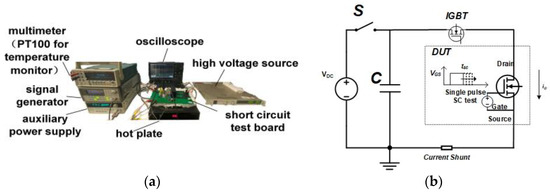
Figure 5. (a) Short-circuit test bench. (b) Schematic diagram of the SC test board.
3. Results
3.1. Short-Circuit Capability of SiC MOSFETs with Different JFET Widths at 400 V
The on and off gate-source voltages (VGS) are 20 and −5 V, respectively. The bus voltage is 400 V, and the short-circuit duration time is increased with a step of 0.5 μs until the device fails. The last non-destruction short-circuit current waveforms for different device designs are illustrated in Figure 6a. According to the figure, the SCWT of Device A1, A2, A3, A4, and A5 are 19.0, 18.5, 17.0, 15.0 and 14.0 μs, respectively. Device A3 with WJFET = 3.0 μm demonstrates the highest peak current due to the lowest on-resistance, as discussed in Section 2.
On the other hand, the SCWT gradually decreases with the increase in WJFET. The changes in peak current and SCWT with WJFET are summarized in Figure 6b. The typical waveform of gate voltage and drain current for the destruction test are shown in Figure 6c. After the destruction test, it is observed that the gate is shorted to the source terminal for all five devices. When the WJFET is increased from 2.0 to 3.0 μm, devices with wider WJFET exhibit higher peak currents.
The higher peak currents result in increased energy dissipation, which can lead to a rapid rise in junction temperature and a reduction in SCWT. However, when JFET width is further increased from 3.0 to 5.0 μm, both the peak current and SCWT decrease. It is evident that wide WJFET design devices are likely to experience different failure mechanisms compared to devices with narrower WJFET designs.
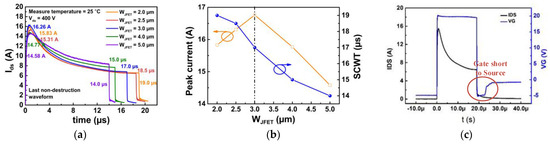
Figure 6. (a) The SC current waveforms of five types of devices with different JFET widths at Vds = 400 V. (b) Extracted SC peak current and SCWT in devices with varied JFET widths. (c) Failure waveform including gate and drain waveforms.
The failure mode is checked with blocking characteristic measurements after device failure, which are shown in Figure 7. After device failure, Device A2 with WJFET = 2.5 μm remains almost the same blocking voltage (Figure 7a) as a fresh device, while Device A5 with WJFET = 5.0 μm shows degraded blocking capability (Figure 7b). OBIRCH (Optical Beam Induced Resistance Change) is utilized to find out the failure spot.
The failure spot in Device A2 is located in the active region, as shown in Figure 8a. FIB (Focus Ion Beam) analysis is employed to observe the cross-section at the failure spot. Figure 8b displays the obtained cross-sectional result of Device A2. Cracks are observed in the ILD (interlayer dielectric) between gate polysilicon and source metal in Device A2. However, for Device A5, different observations are shown. The failure spot is also observed in the active region, as shown in Figure 8c. When the device is stripped in solvents to expose the SiC layer’s surface, a burn mark is found between the JFET region and the channel region. The top view of the device is illustrated in Figure 8d.
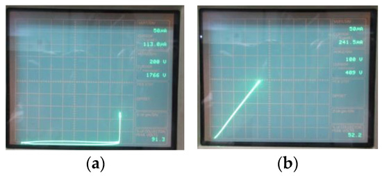
Figure 7. Blocking characteristic after short-circuit failure. (a) Device A2 with WJFET = 2.5 μm. (b) Device A5 with WJFET = 5.0 μm.
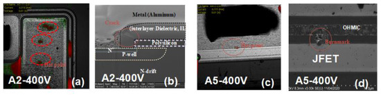
Figure 8. (a) The hot spot is observed under OBIRCH (Optical Beam Induced Resistance Change) of Device A2 at drain voltage of 400 V. (b) The cross-section at hot spot is prepared by FIB (Focus Ion Beam) of Device A2 at drain voltage of 400 V. (c) The hot spot is observed on Device A5 at drain voltage of 400 V. (d) Top view of the failure spot of Device A5 at drain voltage of 400 V after the ILD and top metal is dissolved.
To explain the failure mechanism, the TCAD is used to simulate the short-circuit procedure in SiC MOSFETs. The SiC/SiO2 interface mobility model is established, taking into account the presence of interface traps. The integration of the interface trap is coulomb charge named Nc. Varying the interface trap density at the SiC/SiO2 interface leads to differences in the short-circuit current waveform, as demonstrated in Figure 9a.
With the lower interface trap density, the peak current is higher, and more heat is generated in the SiC MOSFET. The interface trap distribution is determined by extracting the interface trap from the MOS capacitance. Figure 9b shows the comparison between the simulation results (using Dit = 3 × 1011 cm−2eV−1) and the corresponding measurement results. The simulation model is established and the temperature can be extracted through the simulation.
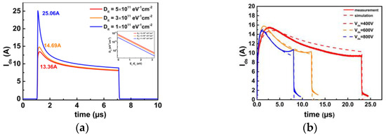
Figure 9. (a) Different interface trap density is established by applying coulomb scattering considering interface trap model. (b) Comparison between measurement and simulation result by using proper model.
For Device A2, the cracks found at ILD are due to the unmatched coefficient of thermal expansion (CTE) between different materials [17]. With higher temperatures, the CTE becomes larger [18,19]. The temperature distribution during the SC procedure at the ILD corner is calculated using a simulation tool, and the result is shown in Figure 10. Consequently, the dominant failure mechanism is the junction temperature rise caused by the energy dissipation within the device during the short-circuit pulse.
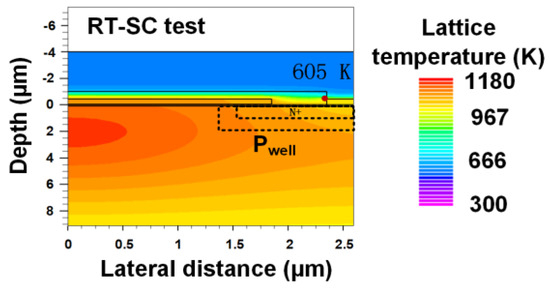
Figure 10. Simulated ILD and source metal temperature during the SC procedure.
For Device A5, the failure mode could be different. To investigate the failure mode, the short-circuit transient process is simulated using TCAD. Due to the wide WJFET design, the electrical field at SiC surface (upper in JFET region) is higher than that in Device A2, resulting in a higher impact ionization. The impact ionization within Device A5 is shown in Figure 11a. Higher impact ionization leads to an increase in hole and electron current densities. A comparison of the hole and electron current densities can be seen in Figure 11b. As the electric field direction points from SiC to the gate in the JFET region, the holes would inject into the gate oxide due to the combined effect of electric field and high kinetic energy resulting from the elevated temperature.
Additionally, in the channel region, the channel electron density in Device A5 is also higher than that in Device A2. Both the holes in the JFET region and electrons in the channel region have the potential to degrade the gate oxide and lead to device failure. To identify the main reason, a repetitive short-circuit test is conducted. The voltage shift direction indicates whether there is hole injection (negative shift) or electron injection (negative shift).
Device A2 and Device A5 are measured during a repetitive short-circuit test with Vds = 400 V, a pulse width of 6µs and Vgs,on/Vgs,off = 19 V/−5 V. When the cycle time is low, the device with a wider JFET width is influenced more by hole injection than electron injection, as observed in the comparison of the two devices in Figure 12a. However, Device A2 is primarily affected by electron injection. With repetitive cycle increasing, the electron injection becomes dominant due to the hot electron effect, as shown in Figure 12b.
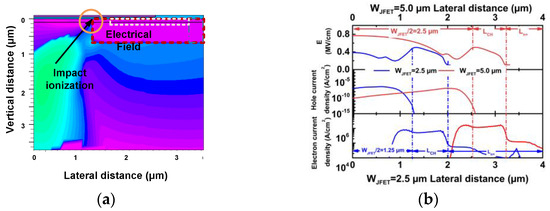
Figure 11. (a) Impact ionization in Device A5 WJFET = 5.0 μm. (b) Comparison of electrical field and hole current density at surface between Device A2 (WJFET = 2.5 μm) and Device A5 (WJFET = 5.0 μm).
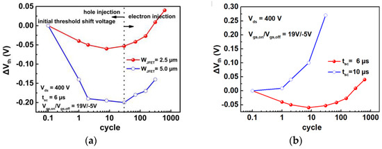
Figure 12. (a) Threshold voltage shift of device with different WJFET after repetitive short-circuit test. (b) Threshold voltage shift for different short-circuit pulse widths (6 and 10 μs).
3.2. Short-Circuit Capability of SiC MOSFETs Measured at Elevated Temperature
Short-circuit tests are carried out at an ambient temperature of 100 °C to verify the failure mechanisms for Device A2 and Device A5. The SC current waveforms are shown in Figure 13a. The peak current and SCWT for the five WJFET designs are extracted from the figure and summarized in Figure 13b. The correlations between SC peak current (SCWT) and WJFET observed at 100 °C are similar to the results obtained at 25 °C (refer to Figure 6b).
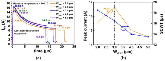
Figure 13. (a) The SC current waveforms of five types of devices with different JFET widths at Vds = 400 V at elevated temperature (100 °C). (b) Extracted SC peak current and SCWT in devices with varied JFET widths at elevated temperature (100 °C).
To study the impacts of ambient temperature on SCWT test results for different WJFET designs, the results obtained at 25 °C and 100 °C test conditions are compared in Figure 14a. The results indicate that wide WJFET designs (WJFET ≥ 3 μm) exhibit an increase in SCWT at elevated temperatures—namely, SCWT demonstrates a positive temperature coefficient for wide WJFET designs.
The increase in SCWT can be attributed to reduced electron injection into the gate oxide at elevated temperatures. Figure 14b compares the short-circuit current waveforms for the 25 and 100 °C test conditions, with tsc = 3 μs used as an example. The peak current at 100 °C is lower than that of 25 °C due to the limitations of acoustic scattering at elevated temperatures, resulting in reduced election injection for the 100 °C test condition.
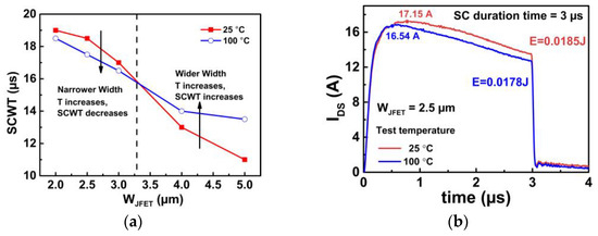
Figure 14. (a) Relationship between SCWT and JFET width under 25 and 100 °C. (b) Comparison of SC current at 25 and 100 °C under the SC duration time of 3 µs.
On the other hand, for narrow WJFET designs (WJFET < 3.25 μm), SCWT decreases at elevated temperatures. The junction temperature is calculated using simulation software. Figure 15 shows the temperature distribution within the device during the short-circuit transient at both 25 °C (Figure 15a) and 100 °C (Figure 15b). Elevated ambient temperatures result in higher junction temperatures. The thermal and mechanical stress can cause cracks in ILD layers, and higher temperatures result in a larger coefficient of thermal expansion mismatch [11].
Thus, the SCWT is decreased at elevated temperatures. In order to figure out whether failure mechanism is changed in the device with wider WJFET, failure spot of Device A4 after SC test under 100 °C is detected shown in Figure 15c. Compared with the results shown in Figure 8b, the ILD crack becomes the main failure reason for the device with wide WJFET.
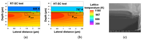
Figure 15. Simulated ILD and source metal temperature during the SC procedure under (a) room temperature and (b) the elevated temperature. (c) The cross-section at hot spot is prepared by FIB (Focus Ion Beam) of Device A5 at drain voltage of 400 V after SC test under 100 °C.
3.3. Short-Circuit Capability of SiC MOSFETs with Different JFET Widths at Varied Vds Measured at Room Temperature
The SC capability of SiC MOSFETs is measured under different bus voltages (400, 600 and 800 V). The short-circuit pulse width (tSC) is gradually increased from 3 μs in steps until DUT fails. The increment step is set to 0.5 μs for 400 V, 0.3 μs for 600 V and 0.1 μs for 800 V, respectively. The short-circuit current waveforms for the five devices tested under a high bus voltage of 800 V are illustrated in Figure 16. The peak current varies among different WJFET designs. For Device A1–A3 with narrow WJFET designs, the peak current is higher than the other two designs, resulting in a shorter SCWT. Additionally, in Device A2, an interlayer crack is observed after the SC test under 800 V in Figure 17a,b.
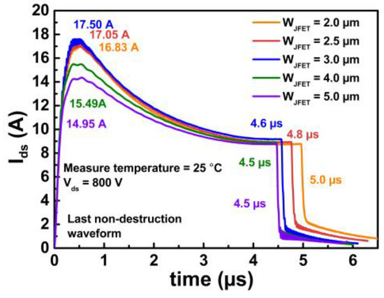
Figure 16. The SC current waveforms of five types of devices with different JFET widths at Vds = 800 V.
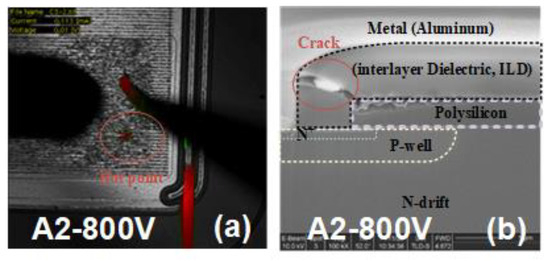
Figure 17. (a) The hot spot is observed under OBIRCH (Optical Beam Induced Resistance Change) of Device A2 at drain voltage of 800 V. (b) The cross-section at hot spot is prepared by FIB (Focus Ion Beam) of Device A2 at drain voltage of 800 V.
The SCWT tested under different bus voltages is summarized in Figure 18a. The energy can be calculated using short-circuit current waveforms and device voltage waveforms. The calculated results are plotted in Figure 18b. Devices with different JFET widths have almost the same SCWT under drain voltages of 600 and 800 V. The WJFET has a significant effect on the SCWT when the drain voltage is 400 V. For higher bus voltage conditions, the difference in SCWT among the five designs is significantly reduced.
In addition, at higher bus voltages, the maximum short-circuit energy that device can safely dissipate is reduced to 33%, as shown in Figure 18b. This is because the short-circuit current multiplied by a high bus voltage generates a significant amount of heat on a very short time scale (<1 μs), causing the device junction temperature to rise rapidly. Thus, the SCWT and total energy are decreased.
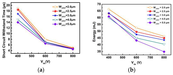
Figure 18. (a) The SCWT of five types of devices with different JFET widths. (b) The SC energy of five types of devices with different JFET widths.
4. Discussion
The on-resistance and short-circuit withstanding time are crucial parameters for SiC MOSFETs, representing their conduction performance and reliability, respectively. It has been reported that the structure designs (JFET region width in this work) can influence both the on-resistance and short-circuit withstanding time. Furthermore, there exists a trade-off relationship between the on-resistance and SCWT, which will be discussed in this section. Figure 19 summarizes the on-resistance and SCWT parameters for each device (Device A1–A5 with different WJFET designs).
The SCWT test results for the three bus voltage conditions (400, 600 and 800 V) are also illustrated in the figure. For each bus voltage, increasing the WJFET from 2 to 3 μm results in a decrease in device on-resistance from 1.68 to a minimum of 1.48 Ω (a reduction of 11.9%). However, a further increase in WJFET will raise the on-resistance, which is unacceptable. On the other hand, observing the SCWT parameters for the 400 V bus voltage condition (red lines in Figure 19), we can observe a slight drop from Device A1 to A3 (11.7%), followed by a significant drop from A3 to A5 (35.2%). The impact of WJFET designs on SCWT is negligible for higher bus voltages.
The bus voltage is usually determined by the power electronic system and circuit designs in practical applications. The saturation current primarily indicates the short-circuit current. The short-circuit current and saturation current are positively correlated. In SiC MOSFETs, the saturation current is influenced by two factors: the JFET region’s pinch-off voltage and the MOSFET channel’s saturation voltage. Short-circuit simulations are used to evaluate the potential under the gate oxide. With a wider JFET width, the potential at the JFET side increases, leading to an increase in channel saturation current due to the Drain-Induced Barrier Lowering effect.
Additionally, a lower pinch-off voltage results in a smaller saturation current in the JFET region. When the JFET region becomes sufficiently narrow, the saturation current of the JFET region becomes the primary factor. For 1200 V–rated SiC MOSFETs, the bus voltage can be selected between 400~800 V or even out of this range. In conclusion, the optimal design of WJFET is 3 μm for the 1200 V SiC MOSFETs studied in this work, without considering an enhanced doping concentration for the JFET region.
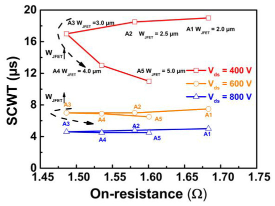
Figure 19. The relationship between on-resistance and SC withstanding time (SCWT) of different devices with varied JFET width.
Under high bus voltage conditions, devices with various JFET widths exhibit similar short-circuit behavior. As the JFET region becomes depleted during the short-circuit test, the resistances in the JFET region become relatively small compared to the channel resistance. Therefore, the JFET width has less impact on the result. Furthermore, it can be concluded that the variation in JFET width is not highly sensitive to the short-circuit withstand capability under high bus voltage, but it exhibits a greater impact under low bus voltage conditions. Moreover, Device A3 demonstrates the best performance within the voltage range of 400 to 800 V.
The relationship between the short-circuit test results at temperatures of 25 and 100 °C and the on-resistance under a 400 V bus voltage is shown in Figure 20 and will be discussed in the following paragraphs. In Section 3.2, the failure reason for DUTs under a high-temperature SC test is clarified. Failure mode is summarized in Figure 21. The failure of a wide WJFET device is due to gate oxide burnout tested in SC under room temperature. As the temperature increases, the failure mode changes to the ILD crack.
When the temperature is above 100 °C, the device failure mode becomes the same. When evaluating the performance of devices operated at high temperatures, the static resistance gradually increases with temperature, while the short-circuit duration time at high temperatures varies. The devices with wider WJFET inhibit the injection of hot electrons at an elevated temperature, thereby reducing the formation of defects caused by hot carriers.
Therefore, there is an improvement in SCWT. When the width of the JFET is less than 3.0 μm (A3), due to the increase in the junction temperature in the high-temperature test, the temperature in the interlayer dielectric reaches the critical value faster, resulting in a reduction in the short-circuit withstand time. If the temperature rises to 150 °C, the SCWT for WJFET devices may all decrease due to the failure mode being changed to the ILD crack mode.
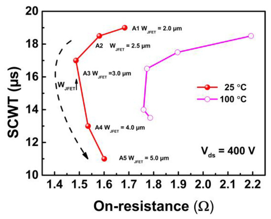
Figure 20. The relationship between on-resistance and SC withstanding time (SCWT) of devices with varied JFET width at 25 and 100 °C.
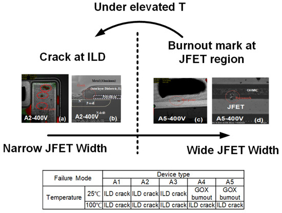
Figure 21. Summary of the failure mode of devices with different WJFET.
Judging from the trade-off relationship between the on-resistance and short-circuit current at room temperature and high temperature, devices with WJFET larger than 3.0 μm are more suitable for operating at high temperatures. These devices exhibit a gradual increase in resistance at high temperatures, resulting in an improved short-circuit performance to a certain extent.
5. Conclusions
In this paper, 1200 V SiC MOSFETs with various WJFET are fabricated, followed by a comprehensive comparison and study of the short-circuit robustness of these devices. Devices with narrow and wide WJFET exhibit distinct failure mechanisms. The ILD crack is observed in the device with narrow WJFET, while the breakdown of gate oxide is found in the device with wider WJFET after device failure. The relationship between on-resistance and SCWT of devices A1–A5 with different JFET widths is summarized.
Device A3 demonstrates the best performance in terms of SCWT and on-resistance characteristics, making it an improved design. Furthermore, devices with narrowed JFET widths have limitations in improving SCWT (<20 μs) under a bus voltage of 400 V. The relationship between the short-circuit test results at temperatures of 25 and 100 °C and on-resistance under a bus voltage of 400 V is also investigated. Devices with WJFET larger than 3.0 μm exhibit improved SCWT under high temperatures and are better suited for high temperature operation. As the temperature rises, their resistance shows a slow increment, contributing to an enhanced short-circuit performance to a certain degree.
Authors
Hongyi Xu, Baozhu Wang, Na Ren, Hu Long, Kai Huang and Kuang Sheng
Original – MDPI
-

Toshiba Electronic Devices & Storage Corporation will move its semiconductor business unit and its research and development (R&D) center to a new building in Toshiba Corp’s Komukai Complex in Kawasaki. It will also be home to Toshiba’s Corporate R&D Center, strengthening synergy within Toshiba Group’s R&D organizations.
The new building will provide spaces for exhibitions and other events open to people from outside the company, as well as collaboration spaces for co-creation with customers. It will create an environment customers can feel free to visit, and promote new ways of working unconstrained by typical workplace limitations.
Virtually all energy will be derived from renewable, and CO2 emissions from power consumption will target zero, contributing to the realization of carbon neutrality.
Division names: Semiconductor Division and Electronic Devices & Storage R&D Center
Address: 1, Komukai-Toshiba-cho, Saiwai-ku, Kawasaki, Kanagawa 212-8583, Japan
Phone number: +81-44-548-2000 (switchboard; no change)
Relocation date: January 22, 2024The address of the Storage Products Division and the company’s registered address remain unchanged, as below.
Storage Products Division
8, Shinsugita-cho, Isogo-ku, Yokohama, Kanagawa 235-8522, JapanRegistered headquarters
1-1, Shibaura 1-Chome, Minato-ku, Tokyo, JapanOriginal – Toshiba
-

STMicroelectronics has signed a long-term silicon carbide (SiC) supply agreement with Li Auto, a leader in China’s new energy vehicle market that designs, develops, manufactures, and sells smart premium electric vehicles. Under this agreement, STMicroelectronics will provide Li Auto with SiC MOSFET devices to support Li Auto’s strategy around high-voltage battery electric vehicles (BEVs) in various market segments.
As the automotive industry transforms towards electrification and decarbonization, high-voltage BEVs have become a popular choice for car makers. These vehicles offer outstanding energy efficiency and extended mileage. Li Auto, known for its extended-range electric vehicles (EREVs), is entering the BEV market with its first-ever high-tech flagship family MPV BEV model premiered in Q4 2023. With plans to introduce more high-voltage BEV models soon, Li Auto will require high volumes of SiC MOSFETs that it will integrate into its traction inverters to ensure superior electric-vehicle performance.
ST’s SiC devices increase performance and efficiency through higher switching frequencies, breakdown voltages, and thermal resistance. These are all particularly critical characteristics at the higher operating voltages required for battery electric vehicles. Li Auto is adopting ST’s advanced third-generation 1200V SiC MOSFET in the traction inverter of its upcoming 800V BEV platform, to ensure industry-leading process stability and performance, efficiency, and reliability.
“Li Auto is committed to providing families with premium EVs exceeding their expectation. This agreement with ST stands as a testament to Li Auto’s unwavering dedication in BEV product development. Collaborating with the renowned global leader in SiC technologies, we anticipate a forthcoming relationship filled with innovation and success,” said Qingpeng MENG, Vice President of Supply Chain, Li Auto.
Holding more than 50% market share in SiC MOSFETs worldwide, ST’s SiC technology has earned high praise from top OEMs for its electric-vehicle performance. It is widely used in onboard chargers and power modules.
“As a world leader in power devices and wide bandgap semiconductor technologies, ST has established long-term supply agreements with major car makers and Tier 1 suppliers. The SiC supply agreement with Li Auto marks a significant step building upon our existing long-term relationship in other automotive applications,” said Henry CAO, Executive Vice President of Sales & Marketing, China Region, STMicroelectronics. “ST is committed to supporting Li Auto’s ambition to become a top premium electric vehicle brand in China, offering their customers superior vehicle performance and range with our innovative SiC technologies.”
Original – STMicroelectronics
-

Teledyne e2v HiRel announced the addition of new space screened versions of its popular 100 V, 90 A and 650 V, 30 A high reliability gallium nitride high electron mobility transistors (GaN HEMTs).
- TDG650E30BSP
- TDG100E90BSP
- TDG100E90TSP
The new parts go through NASA Level 1 or ESA Class 1 screening flow and can be brought up to full Level 1 conformance with extra qualification testing if desired. Typical applications include battery management, dc-dc converters, and space motor drives.
Two new 100 V parts are available with both bottom-side and top-side cooled packaging. One new 650 V 30 A GaN-on-Silicon power transistor is available in a bottom-side cooled package. Each device is available with options for EAR99 or European sourcing.
Teledyne e2v HiRel’s GaN HEMTs feature single wafer lot traceability, extended temperature performance from -55 to +125°C, and low inductance, low thermal resistance packaging.
“Our customers have embraced the previous release of 650 V space screened devices, and we have expanded our portfolio to provide additional options. These GaN HEMT products save customers time and money by providing standard devices without the need for additional screening.” said Mont Taylor, VP of Business Development for Teledyne e2v HiRel. “Our expanded catalog with standard burn-in make it easy for designers to utilize the latest in GaN in their designs.”
Gallium nitride devices have revolutionized power conversion in other industries and are now available in radiation tolerant, plastic encapsulated options that have undergone stringent reliability and electrical testing to help ensure mission critical success. The release of these new GaN HEMTs delivers to customers the efficiency, size, and power-density benefits required in critical aerospace and defense power applications.
Original – Teledyne e2v HiRel
-

Navitas Semiconductor held an Opening Ceremony and 2023 Investor Day at its new headquarters in Torrance, CA.
Torrance Mayor, George Chen, and Dustin McDonald from the Office of the Governor of California joined Navitas’ CEO and co-founder Gene Sheridan to speak and cut the ribbon, officially opening Navitas’ new headquarters. Around 100 highly-skilled Navitas staff are employed in Torrance for all aspects of GaN and SiC design, applications, test, characterization and quality plus finance, marketing and HR. Further team growth is planned for 2024, including a $20M investment to add SiC epi-growth capability for strategic manufacturing expansion.
The well-attended investor meeting began with Mr. Sheridan’s recap on a year of significant growth for Navitas, with a doubling of revenue, a $92M capital raise, four major new technology platforms and an update on Navitas’ mission to ‘Electrify Our World™. Then, Mr. Sheridan outlined a $1.3T electrification market opportunity as GaN and SiC enable and accelerate our transition away from fossil fuels to a carbon-neutral, full-electrified world, envisaged as ‘Planet Navitas’.
Dan Kinzer, co-founder and COO/CTO then introduced technology platforms including Gen-4 GaNSense half-bridges for motor drive and mobile fast chargers, GaNSafe – the world’s most protected GaN powertrain, GaNSense Control, and a revolutionary new bi-directional GaN power IC platform with up to 9x smaller chip size than legacy silicon MOSFETs or IGBTs. Sid Sundaresan, SVP for the GeneSiC product line added more detail on the Gen-3 Fast SiC platform.
In May, Navitas announced a qualified customer pipeline of $760M, across mobile, solar/ESS, EV/eMobility, data center and appliance/industrial markets. At the Investor Day, David Carroll, SVP Worldwide Sales announce that the pipeline had increased by 65% to $1.25B, with 10/10 top mobile OEMs and majority of solar inverter makers. Investors also heard from the voices of Navitas customers, including Rick Liu from Accopower for EV, Belkin’s Steve Malony for mobile, Philipp Guo from VREMT for EV, Adam Weissman from Anker for mobile, and Harron Inam from DG Matrix for EV roadside charging.
Ron Shelton, Navitas CFO, presented more detail on the impressive financial results with increased gross margin, and over $170M is cash and no debt, plus a long-term target to grow 6x-10x more than the market, with 50%+ gross margins.
In-person visitors then toured the Navitas facility, including past & present demos and the ‘Electrify Studio’ experience – where Navitas is creating a vision for our electrified planet – plus SiC design, GaN IC design, applications, test & characterization, quality & reliability.
The day concluded with a celebration at the Crypto.com Arena, where guests enjoyed the LA Clippers’ victory—a fitting finale to a day filled with inspiration, innovation, and collaboration.
Comprehensive Investor Day material is available via the Navitas website, with presentation slides, and complete video playback of the main presentations, customer testimonials, and facility tour.
Original – Navitas Semiconductor
-

Due to the positive development of the market capitalization, the Siltronic share is rejoining the MDAX index today. After several months in the SDAX, the Siltronic AG share is once again represented in the second most important index of the German stock exchange. Additionally, Siltronic shares will remain part of the TecDAX.
Throughout the year, Siltronic’s share price was negatively impacted by the market weakness in the semiconductor industry, which led to its descent to the SDAX in June 2023. Since then, the share price has steadily recovered, and the company’s market capitalization has increased significantly.
Dr. Michael Heckmeier, CEO of Siltronic, commented on this development: “The re-inclusion of Siltronic in the MDAX reflects investors’ confidence in our future prospects and our continued growth. This underscores the robust share price performance of recent months.”
Siltronic’s inclusion in the MDAX is part of Deutsche Börse AG’s regular quarterly review. The decision is based on the market capitalization of the freely tradable shares, i.e. the free float market capitalization.
Original – Siltronic
-

Infineon Technologies AG announced its commitment to set a science-based target. By that Infineon expands its climate strategy even further. The company is very well on track towards CO2-neutrality by 2030, relating to its direct and indirect energy related emissions (Scope 1 and 2).
After having already reduced these emissions by 56.8 percent to date versus the base year of 2019, Infineon now sets itself even more ambitious targets by involving the supply chain (Scope 3) in the company’s climate protection efforts.
“Decarbonization is a guiding principle for Infineon. We have made great progress. With our commitment to set a science-based target, we are taking the next important step, adhering to the widely respected global standard for tackling climate change”, said Elke Reichart, Chief Digital Transformation Officer and responsible for Sustainability at Infineon. “We are actively inviting our suppliers to join us on our journey by setting their own carbon reduction targets. To truly address climate change, collaboration across the entire value chain, transparent and comprehensive data as well as global standards are foundational.”
Infineon has doubled its revenue since 2019 and halved its CO2 emissions (Scope 1 and 2) at the same time. The main drivers for lowering emissions are energy efficiency measures, comprehensive PFC abatement measures and switching its operations to renewable energy, which makes proportionally the largest contribution.
In 2023, Infineon reaches another key milestone in this respect. The two largest manufacturing sites in Asia – Kulim and Melaka in Malaysia – have now transitioned to green electricity, following the switch to renewables at its European and North American sites in 2021 and 2022 respectively.
The Science Based Targets initiative (SBTi) serves as a benchmark for ambitious climate action in the private sector. The initiative provides a clearly defined pathway for companies to reduce greenhouse gas (GHG) emissions. Targets are considered ‘science-based’ if they are in line with the latest climate science in order to meet the goals of the Paris Agreement – limiting global warming to well below 2°C above pre-industrial levels and pursuing efforts to limit warming to 1.5°C. SBTi is a partnership between the Carbon Disclosure Project (CDP), the United Nations Global Compact, World Resources Institute (WRI) and the World Wide Fund for Nature (WWF).
In 2020, Infineon had set its carbon neutrality target 2030 (Scope 1 and 2 emissions) already in line with science-based target requirements. With the expansion of its climate strategy to include Scope 3, Infineon is working closely together with supply chain partners and is putting special emphasis on further improvements in data availability and accuracy.
Original – Infineon Technologies
-

Dr. Christian Kranert, Group Manager Equipment and Defect Simulation of the Materials Department at Fraunhofer IISB, developed a new software for the fast, full-wafer and automated detection and classification of crystal defects in silicon carbide (SiC) substrates. He also pushed the licensing of his new, so-called x-ray ropography (XRT) toolbox to the users of the x-ray topography measuring device XRTmicron from Rigaku. Another highlight is the establishment of two new SEMI International Standards for 4H-SiC defect quantification using XRT test methods.
These outstanding results confirm the success of the Joint Labs model at Fraunhofer IISB. Joint Labs are an exclusive opportunity to collaborate with Fraunhofer IISB in an industry-compatible laboratory environment.
Rigaku Europe SE and Fraunhofer IISB are operating the Center of Expertise for X-ray Topography, a joint lab that is located at the IISB’s headquarters in Erlangen, Germany. This fruitful collaboration is vividly illustrated by the new business in the field of SiC wafer mapping, which Rigaku has built up around its XRTmicron product line in less than two years.
The new LZE Prize honors Fraunhofer IISB employees for exceptional achievements. The LZE Prize is awarded for outstanding acquisitions or particularly successful collaborations, new networks with domestic and foreign partners or above-average achievements in the transfer of know-how from research to industry. The Leistungszentrum Elektroniksysteme (LZE) is a joint initiative of the Fraunhofer-Gesellschaft, Fraunhofer IIS, Fraunhofer IISB, and FAU Erlangen-Nürnberg (FAU), together with industry partners and further research institutes.
Original – Fraunhofer IISB
