-
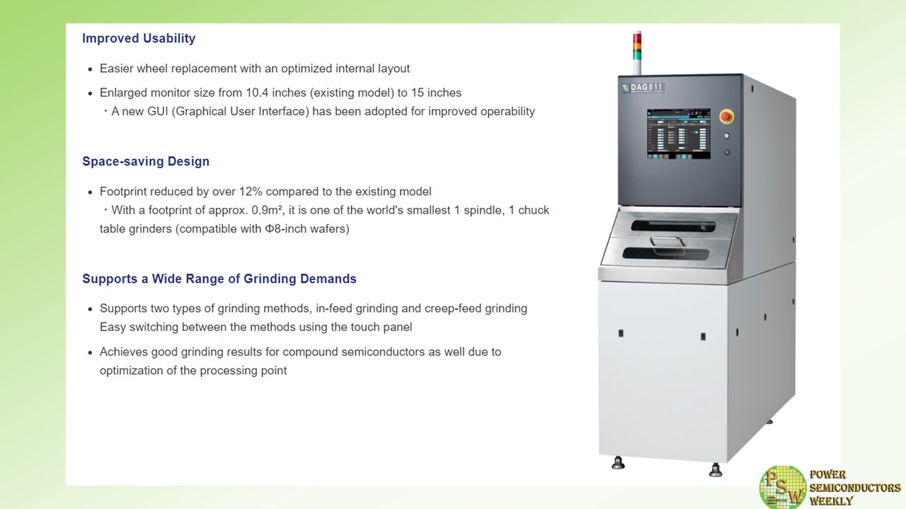
DISCO Corporation has developed DAG811, which has improved usability and a space-saving footprint, as the successor to DAG810, an automatic grinder that has responded to a wide range of needs and has been well received for many years. This equipment is being exhibited at SEMICON Japan 2023 (December 13-15, Tokyo Big Site).
Since its release in 2002, DAG810 has been used for R&D and semi-mass production in a wide range of fields such as semiconductors, electronic components, and optical components. In response to the increasing demand related to applications, DAG811 was developed upon renewing the equipment specifications such as improving the operability and making it compact.
By optimizing the processing point, this equipment also meets the grinding needs of compound semiconductors such as SiC and GaN used in power devices, for which demands are increasing.
Features
Improved Usability
- Easier wheel replacement with an optimized internal layout
- Enlarged monitor size from 10.4 inches (existing model) to 15 inches
・A new GUI (Graphical User Interface) has been adopted for improved operability
Space-saving Design
- Footprint reduced by over 12% compared to the existing model
・With a footprint of approx. 0.9m², it is one of the world’s smallest 1 spindle, 1 chuck table grinders (compatible with Φ8-inch wafers)
Supports a Wide Range of Grinding Demands
- Supports two types of grinding methods, in-feed grinding and creep-feed grinding
Easy switching between the methods using the touch panel - Achieves good grinding results for compound semiconductors as well due to optimization of the processing point
Original – DISCO
-
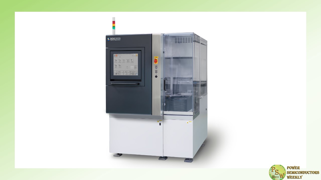
DISCO Corporation has developed DDS2020, a fully automatic die separator that supports Φ200 mm tape frames and achieves separation of hard materials including SiC and sapphire. This equipment is being exhibited at SEMICON Japan 2023 (December 13-15, Tokyo Big Site).
Stealth dicingTM is a dicing process where a modified layer is formed by focusing a laser beam inside the workpiece, following which stress is applied externally to separate it into die. As silicon wafers can be separated with a relatively small amount of stress, the die can be separated by simply expanding the dicing tape. On the other hand, materials that have high mechanical strength like SiC wafers that are widely used for power devices and sapphire wafers used for LED cannot be separated just by expansion. Thus, a breaking mechanism was necessary.
DDS2020 is a die separator that achieves separation of hard materials such as SiC and sapphire with a low load using a new breaking mechanism.
Features
- New breaking mechanism that achieves low load separation
- Load decreased by 40% compared to the conventional breaking mechanism
- Breaking load measurement and graph display
- Detects unseparated die and improves the yieldAutomatic retry setting when unseparated die are detected is also available
- Tape frame remounting for breaking is no longer necessary
- Eliminates remounting work and reduces tape costs
Original – DISCO
- New breaking mechanism that achieves low load separation
-

Axcelis Technologies, Inc. announced shipment of multiple Purion H SiC Power Series™ and the Purion M SiC Power Series™ ion implanter systems to leading power device chipmakers in Europe and Asia, and the closure of an Purion H200 SiC Power Series™ evaluation tool in Europe. Shipments include both evaluation and revenue systems and will be used in high volume production of power devices supporting automotive industry electric vehicle (EV) applications.
President and CEO of Axcelis Technologies Russell Low commented, “The power device market continues to grow rapidly and is a major driver of our growth globally. We are pleased to continue to support our customers’ fab capacity expansion and also excited about the opportunity to support our new customers with our market leading Purion Power Series ion implanters.”
Axcelis is the only implant supplier in the industry to offer a comprehensive solution to our power device manufacturing customers. The Purion Power Series™ family is uniquely suited to excel at power device applications due to its innovative platform that offers the flexibility to handle multiple wafer sizes (150mm, 200mm and 300mm), various substrate types (SiC, Si IGBT, GaN, and GaAs wafers) at various implant temperatures (cold, room temperature, warm and hot).
This is accomplished while delivering the industry’s highest throughput and capital efficiency. The Purion Power Series™ covers the full ion implant market space with the Purion H Purion Power Series™ for high current applications, the Purion H200 Power Series™ for high current medium energy applications, Purion M Power Series™ for medium current applications and the Purion XE Power Series™ for high energy applications.
Original – Axcelis Technologies
-
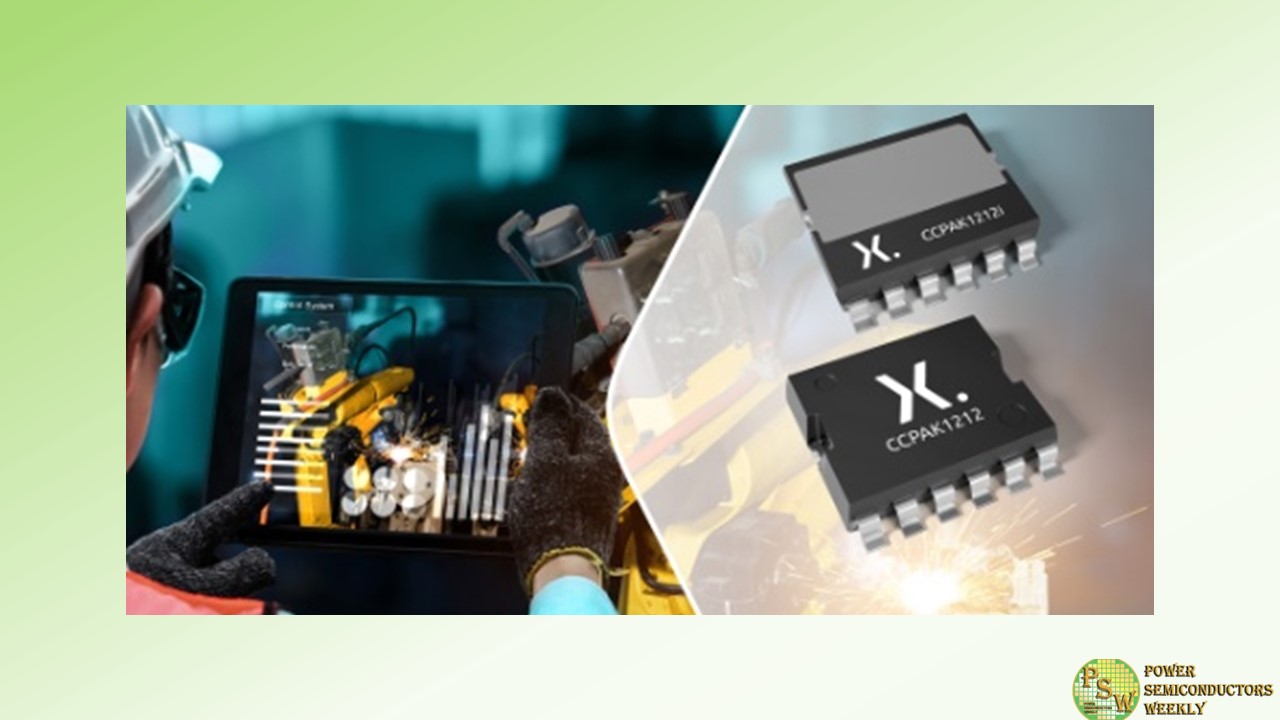
Nexperia announced that its GaN FET devices, featuring next-gen high-voltage GaN HEMT technology in proprietary copper-clip CCPAK surface mount packaging, are now available to designers of industrial and renewable energy applications.
Building on two decades of expertise in supplying high-volume, high-quality copper-clip SMD packaging, Nexperia is now proud to extend its revolutionary packaging approach to GaN cascode switches in CCPAK. The GAN039-650NTB, a 33 mΩ (typ.) Gallium Nitride (GaN) FET within the CCPAK1212i top-side cooling package, ushers in a new era of wide bandgap semiconductors and copper-clip packaging.
This technology offers advantages for renewable energy applications such as solar and residential heat pumps, further enhancing Nexperia’s commitment to developing the latest component technology for sustainable applications. It is also suited to a wide spectrum of industrial applications such as servo drives, switched-mode power supplies (SMPS), server, and telecom.
Nexperia’s CCPAK surface mount packaging uses Nexperia’s proven innovative copper-clip package technology to replace internal bond wires. This reduces parasitic losses, optimizes electrical and thermal performance, and improves device reliability. For maximum flexibility in designs, these CCPAK GaN FETs are available in top- or bottom-cooled configurations to further improve heat dissipation.
The cascode configuration of the GAN039-650NTB enables it to deliver superior switching and on-state performance, with a robust gate offering high margins against noise. This feature also simplifies application designs by eliminating the requirement for complex gate drivers and control circuitry, instead allowing them to be conveniently driven using standard silicon MOSFET drivers.
Nexperia’s GaN technology improves switching stability and helps to shrink die size by approximately 24%. In addition, device RDS(on) is reduced to only 33 mΩ (typ.) at 25°C, with a high threshold voltage and low diode forward voltage.
“Nexperia recognizes that designers of industrial and renewable energy equipment need a highly robust switching solution that can provide excellent thermal efficiency when performing power conversion.”, according to Carlos Castro, Vice President and General Manager of the GaN FET business at Nexperia. “This is why Nexperia decided to bring together the exceptional switching performance of its cascode GaN FETs with the exceptional thermal properties of its CCPAK packaging to offer customers a compelling solution.”
Nexperia begins its CCPAK portfolio release with the top-cooled 33 mΩ (typ.), 650 V GAN039-650NTB, and will follow shortly with the bottom-cooled variant, GAN039-650NBB of the same RDS(on). More information including datasheets and samples is available at www.nexperia.com/ccpak.
Original – Nexperia
-

Infineon Technologies has once again been included in the Dow Jones Sustainability™ World Index, as announced by S&P Global last Friday in New York, USA.
“We are proud that Infineon has been chosen as one of the world’s most sustainable companies for the 14 th consecutive year“, said Elke Reichart, Member of the Board and Chief Digital Transformation Officer, responsible for Sustainability at Infineon. “Moreover, we feel strongly encouraged to keep up our efforts at making further progress towards our ambitious sustainability goals. Therefore, we are continuously developing our processes and drive innovation within the company and beyond. The green and the digital transformation go hand in hand.”
Infineon is well on track with the implementation of its CO 2-neutrality goal by 2030 (Scope 1 and 2). To date emissions have been reduced by 56.8 percent compared with the base year of 2019 while approximately doubling the business at the same time.
As a leading manufacturer of semiconductors for power electronic systems and the IoT, Infineon makes a significant contribution to decarbonization on the way to a net-zero society. Infineon’s products and solutions help to save 34 times more CO 2 emissions over the course of their usage than were created during their production.
This year, Infineon scored especially well in Privacy Protection and Innovation Management that includes aspects like Research & Development, Product Innovation and also Process Innovation, for instance through digitalization and the application of Industry 4.0 principles.
The Dow Jones Sustainability Index is regarded as one of the most important benchmarks for sustainability and lists the world’s leading companies from 61 industries. The assessment is based on the companies’ economic, environmental and social performance. Its objective is to help investors make informed decisions on how to align their portfolios more clearly with sustainability aspects, and to encourage companies to actively continue their efforts in this regard.
Original – Infineon Technologies
-
A plan by ROHM Co., Ltd. and Toshiba Electronic Devices & Storage Corporation to collaborate in the manufacture and increased volume production of power devices has been recognized and will be supported by the Ministry of Economy, Trade and Industry as a measure supporting the Japanese Government’s target of secure and stable semiconductor supply.
ROHM and Toshiba Electronic Devices & Storage will respectively make intensive investments in silicon carbide (SiC) and silicon (Si) power devices, effectively enhance their supply capabilities, and complementally utilize other party’s production capacity.
Power devices are essential components for supplying and managing power supply in all kinds of electronic equipment, and for achieving a carbon-free, carbon-neutral society. Current demand is expected to see continued growth.
In automotive applications, development of more efficient, smaller and lighter electric powertrains has advanced alongside the rapid expansion in vehicle electrification. In industrial applications, stable supply of power devices and improved characteristics are widely required to support increasing automation and higher efficiency requirements.
Against this backdrop, ROHM has formulated a management vision, “We focus on power and analog solutions and solve social problems by contributing to our customers’ needs for energy savings and miniaturization of their products.,” and accelerates its efforts for a carbon-free. SiC power devices are the keys to energy savings.
Since the world’s first mass production of SiC MOSFETs, ROHM has been constantly developing industry-leading technologies. Among these are ROHM’s latest 4th Generation SiC MOSFETs that will be adopted for numerous electric vehicles and industrial equipment. As one of its priority projects, ROHM is working on SiC business, which contains aggressive and continuous investment to increase the production capacity of SiC and meet strong demand growth.
Toshiba Group, with its long-standing Basic Commitment, “Committed to People, Committed to the Future.,” aims to advance the achievement of carbon neutrality and a circular economy. Toshiba Electronic Devices & Storage has for decades supplied Si power devices, mainly for automotive and industrial markets, that have helped to secure energy saving solutions and equipment miniaturization.
The company started production on a 300mm wafer line last year, and is accelerating investment to enhance production capacity and meet strong demand growth. It is also advancing development of a wider lineup of SiC power devices, especially for automotive and power transmission and distribution applications, taking full advantage of the expertise it has cultivated in railway vehicle applications.
ROHM has already announced its participation in the privatization of Toshiba, but this investment did not serve as the starting point for manufacturing collaboration between the two companies. Under intensifying international competition in the semiconductor industry, ROHM and Toshiba Electronic Devices & Storage have been considering collaboration in the power device business for some time, and that resulted in the joint application.
ROHM and Toshiba Electronic Devices & Storage will collaborate in manufacturing power devices, through intensive investments in SiC and Si power devices, respectively, toward enhancing both companies’ international competitiveness. The companies will also seek to contribute to strengthening the resilience of semiconductor supply chains in Japan.
Original – Toshiba
-

Analog Devices, Inc. announced that its Board of Directors has appointed Dr. Peter B. Henry, a renowned international economist, as an independent director and member of the Board’s Audit Committee effective December 5, 2023.
Dr. Henry is currently the Class of 1984 Senior Fellow at the Hoover Institution and Senior Fellow at the Freeman Spogli Institute for International Studies, both at Stanford University. Dr. Henry is also Dean Emeritus of New York University’s Leonard N. Stern School of Business. His appointment expands ADI’s Board to 13 members.
“We are delighted to welcome Peter to the ADI Board,” said Vincent Roche, ADI’s CEO and Chair. “He is an accomplished academic leader and a well-known figure in foreign affairs, global economics, and international finance. We look forward to bringing his significant expertise and global perspective to our Board as we continue to solve our customers’ toughest challenges and enable breakthroughs at the Intelligent Edge.”
Dr. Henry also leads the Ph.D. Excellence Initiative (PhDEI), a post-baccalaureate program designed to address underrepresentation in economics by mentoring exceptional students from underrepresented backgrounds interested in pursuing doctoral studies in the field. For his founding and leadership of the PhDEI, Dr. Henry received the 2022 Impactful Mentoring Award from the American Economic Association.
Dr. Henry currently serves on the Boards of Directors of Citigroup and NIKE, Inc., and as Chair of the Board of the National Bureau of Economic Research. He is a member of the Council on Foreign Relations.
Previously, Dr. Henry served at New York University’s Leonard N. Stern School of Business as the William R. Berkley Professor of Economics and prior to that as Dean. Before that, Dr. Henry was the Konosuke Matsushita Professor of International Economics at the Stanford University Graduate School of Business, where his early research was funded by a National Science Foundation CAREER Award.
Dr. Henry received a bachelor’s degree in economics from the University of North Carolina at Chapel Hill, a bachelor’s degree in mathematics from Oxford University where he was a Rhodes Scholar, and a Ph.D. in economics from the Massachusetts Institute of Technology.
Original – Analog Devices
-
Today some applications tend to increase bus voltage, and using 1200V SiC power modules can no longer correspond to voltage requirements. Using 1700V SiC devices can solve the problem, but it comes with a price.
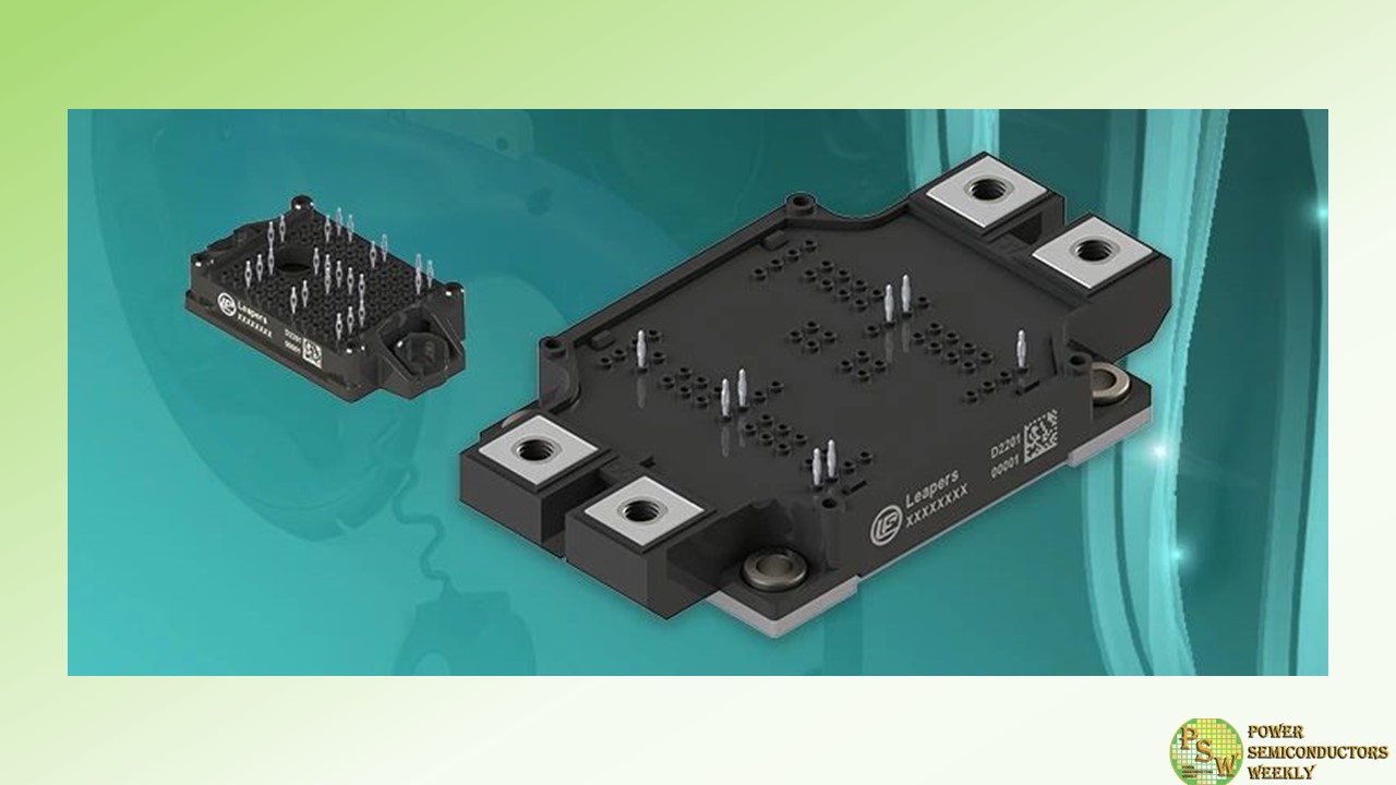
Leapers Semiconductor announced a new series of 1400V SiC power modules in already familiar E0 and ED3S packages. They are the perfect solution to the mentioned problem, providing great performance at affordable price.
At the moment the new series 1400V SiC modules come in Half-Bridge, H-Bridge, and Boost topologies.
Leapers Semiconductor new SiC product family features:
– 1,4kV voltage
– 50 – 600A current
– 3,2 – 40 mOhm Rds(on)
– Epoxy resin
– Si3N4 AMB substrate
– Low thermal resistance
– Low switching lossesFirst batches of 1400V SiC power modules successfully passed field tests by the end customers and soon will be mass used in:
– DC fast chargers
– Commercial EVs
– Power supplies for production of hydrogen
– DC/DC convertersOriginal – Leapers Semiconductor
-

Nexperia announced the successful signing of their USD 800 million equivalent senior Revolving Credit Facility (RCF). The RCF was substantially oversubscribed with participation from a dozen European, Asian and international banks, an indication of the strong support for Nexperia in the loan market. Proceeds will be earmarked towards the refinancing, general corporate and working capital purposes.
The RCF constitutes Nexperia’s first Sustainability Linked Loan (SLL) and includes environmental and social Key Performance Indicators (KPIs) relating to greenhouse gas emissions and gender diversity with a focus on including more women in management positions. The RCF represents Nexperia’s long-lasting commitment to creating a positive impact on society and the environment as it embarks on its next stage of expansion. To further enhance transparency and governance of the SLL, these KPIs are supported by a second party opinion from Sustainalytics and will be independently assured annually by a third party.
Stefan Tilger, Chief Financial Officer of Nexperia, said: “We are delighted with the strong support received from existing and new lenders from across the world, which underscores Nexperia’s operational excellence and global footprint. Earlier this year, Nexperia issued its first Sustainability Report and announced its target of achieving carbon neutrality by 2035. Structuring this financing as a Sustainability-Linked Loan is a reaffirmation of our commitment to Nexperia’s Environmental and Social ambitions.”
Amit Sinha, Global Head of TMT at DBS Bank Ltd., said: “DBS Bank has been a steadfast supporter of Nexperia over the years, and we are grateful for the opportunity to lead this financing as Nexperia embarks on its next growth stage”.
“The strong oversubscription by lenders across Europe and Asia is driven by Nexperia’s market position as global leader in Discretes, Logic and MOSFETs and solid financial standing. The KPIs are a testament to Nexperia’s commitment to foster innovations and creative solutions that add value for our customers, communities, and our planet.”, added Mildred Chua, Group Head of Syndicated Finance at DBS Bank Ltd.
DBS Bank Ltd. acted as Sole Original Mandated Lead Arranger, Bookrunner and Sustainability Coordinator for the RCF. Houthoff London LLP and Clifford Chance LLP acted as the borrower’s and lenders’ legal counsel respectively.
Original – Nexperia
-
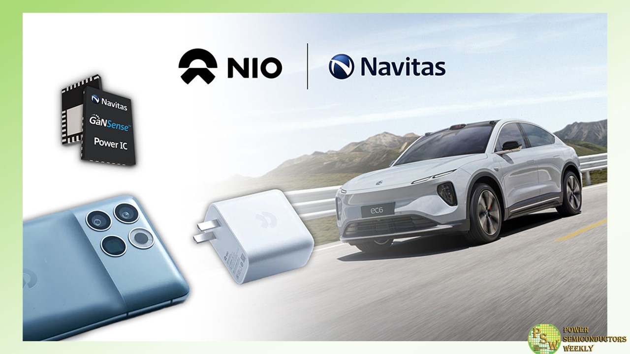
Navitas Semiconductor announced that NIO, a global, leading, new-energy vehicle maker has released its inaugural smartphone, the NIO Phone with a powerful 66 W fast charger featuring Navitas’ next-generation gallium-nitride (GaN) GaNFast™ power ICs equipped with GaNSense™ technology. This enhancement delivers flagship-level charging efficiency, providing end users with a better vehicle-centric mobile interconnection experience. New GaNFast ICs are replacing legacy silicon chips to enable next-gen fast-charging for mobile phones, tablets and laptops.
The flagship NIO Phone features the leading Qualcomm Snapdragon 8 Gen 2 chip, and boasts a 6.81-inch 2K variable refresh-rate curved screen, with the main, ultra-wide-angle, and 50 M pixel periscope telephoto cameras. Using NIO Link panoramic-interconnection technology, the NIO Phone integrates smoothly and seamlessly with smart EVs and NIO’s in-car system. With a single click, the driver can control over 30 functions, and equipped with ultra-wideband technology, it can completely replace traditional car keys.
To support such powerful and comprehensive features, the NIO Phone is equipped with a large 5,200 mAh battery and an in-box GaNFast charger offering up to 66 W of charging power. Measuring only 57 x 57 x 30 mm (97.5 cc), the NV6136 GaNFast power IC in a high-frequency quasi-resonant (HFQR) topology with loss-less current sensing and ultra-fast autonomous short-circuit protection, delivers power density of 1.03 W/cc.
Mr. Zhang Baozhou who is responsible for NIO’s mobile phone supply chain, stated, “NIO is dedicated to providing users with high-performance smart electric vehicles and ultimate user experience, creating a delightful lifestyle for our users.
The NIO Phone fulfills the expectations and needs of NIO users for a flagship smartphone, making their cars more intuitive and user-friendly. In launching NIO Phone, we are very pleased to collaborate with Navitas Semiconductor, industry leader in GaN to utilize the mature, cutting-edge GaNFast power ICs, allowing our users to experience a comprehensive, lightweight, and efficient charging experience.”
Mr. Wu Gongli, GM of R&D for TenPao, the manufacturing partner for the NIO Phone commented, “We are excited to work with Navitas to build this leading GaN charger for NIO users, marking an important milestone in TenPao’s development. Navitas’ GaNFast ICs deliver top power-density performance with easy-to-use features. The combination of high efficiency and fast design accelerates our time-to-market.”
Mr. Yingjie (Charles) Zha, VP and GM of Navitas China, stated, “Navitas is extremely honored to collaborate with TenPao to make the NIO Phone possible by integrating the leading GaNFast technology into the NIO Phone. Navitas’ mission to ‘Electrify Our World™’ aligns closely with NIO’s objective of ‘Blue Sky Coming’. This is just the beginning of our collaboration. In the future, Navitas will spare no effort to deeply-integrate energy-saving, sustainable, world-leading GaN and SiC technology into NIO Phone’s DNA, creating a comprehensive lifestyle revolution from a smartphone to EVs.”
Original – Navitas Semiconductor
