-

Vishay Intertechnology, Inc. announced that it has been honored by DENSO Corporation, a leading mobility supplier, with a 2022 Collaboration Award.
The 2022 Collaboration Awards recognize suppliers that have continued to provide DENSO with key components that keep production lines moving for the company and its customers, despite the tight supply market. Previously this year, Vishay was also recognized by DENSO with a 2022 North America Business Partner of the Year Award in the Quality Leader category.
“Vishay has demonstrated a strong commitment to supporting DENSO on both a working and management level,” said Kouji Arima, CEO of DENSO. “We sincerely appreciate the company’s unsparing efforts and contributions, and know we can count on them regardless of the market situation. We look forward to building an even stronger partnership with Vishay as we continue working together.”
“We are deeply honored to receive this acknowledgment from DENSO of our unwavering support during challenging market conditions,” said Joel Smejkal, President and CEO at Vishay. “This recognition underscores our commitment to operational excellence and the strength of our partnership with the company. We look forward to building on this level of collaboration to grow together in the coming years.”
Original – Vishay Intertechnology
-

Texas Instruments announced its new 300-mm semiconductor wafer fabrication plant in Richardson, Texas, RFAB2, achieved LEED (Leadership in Energy and Environmental Design) Gold certification under version 4 (v4). This designation makes RFAB2 the first wafer fab in the United States and the fourth in the world to achieve this more stringent certification from the U.S. Green Building Council (USGBC) for the sustainable design, construction and operation of high-performance green buildings.
“One of TI’s ambitions is to be a company that our employees are personally proud to be a part of and would want as our neighbor,” said Brian Dunlap, vice president, 300-mm Wafer Fab Manufacturing Operations at Texas Instruments. “We are proud that RFAB2 has achieved LEED Gold v4 certification, underscoring TI’s long-standing commitment to operate in a socially thoughtful and environmentally responsible manner.”
RFAB2, which is TI’s fourth LEED-certified manufacturing plant, was designed to reduce water and electricity usage. In fact, the new fab’s design, construction and operation are expected to achieve significant efficiencies, including saving 750 million gallons of potable water and almost 80,000 megawatt-hours of energy annually. The factory was also constructed using responsibly sourced materials and was designed and built in a way that fosters a healthy work environment.
“What makes this LEED Gold designation impressive is that Texas Instruments achieved this high standard developed for office buildings in a semiconductor manufacturing plant,” said Jill Kurtz, director of Building Sciences at Page, who consulted TI in the certification process. “By prioritizing sustainability and transparency, TI is delivering real impact in water and energy savings, leading the way in their industry and helping USGBC continue toward its goal of green buildings for everyone within this generation.”
The LEED Gold v4 certification solidifies TI’s dedication to responsible, sustainable manufacturing, including multi-year goals and programs focused on conserving natural resources, reducing energy consumption and mitigating environmental impact. To learn more about TI’s commitment to sustainability, download the company’s latest Corporate Citizenship Report.
Original – Texas Instruments
-
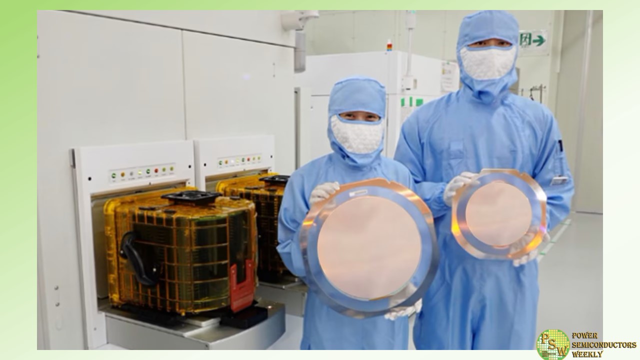
Mitsubishi Electric Corporation has completed installation of its first 12-inch silicon wafer processing line at its Power Device Work’s Fukuyama Factory, which manufactures power semiconductors. In addition, through sample production and testing, it has been verified that the power semiconductor chips processed on this production line achieve the required performance levels.
As previously announced, Mitsubishi Electric is planning to start mass production on the new 12-inch silicon wafer line in fiscal 2025. The company aims to approximately double its silicon power semiconductor wafer processing capacity by fiscal 2026 compared to fiscal 2021 levels.
In recent years, the demand for power semiconductors offering efficient control of electrical power is growing as countries look to achieve carbon-free status. Power semiconductors are utilized in wide range of relevant products, including electric vehicles, consumer devices (e.g. air-conditioning systems), industrial equipment, renewable energy and traction devices, and a stable supply is required in order to meet this growing demand.
Mitsubishi Electric will contribute to the realization of a carbon-free society through enhancement of its production capacity and by ensuring a stable supply of power semiconductors through the introduction of highly efficient 12-inch wafer production lines.
Original – Mitsubishi Electric
-
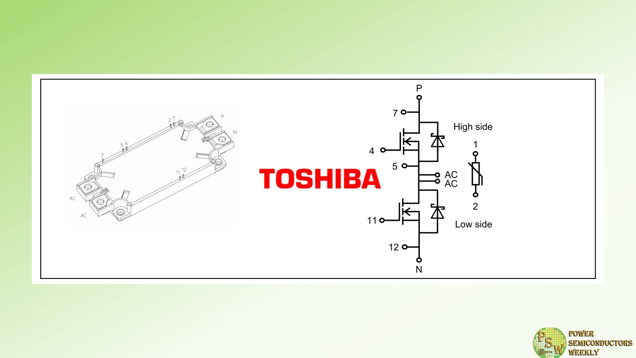
Toshiba Electronic Devices & Storage Corporation developed “MG250YD2YMS3,” the industry’s first 2200V dual silicon carbide (SiC) MOSFET module for industrial equipment. The new module has a drain current (DC) rating of 250A and uses the company’s third generation SiC MOSFET chips. It is suitable for applications that use DC1500V, such as photovoltaic power systems and energy storage systems. Volume shipments start today.
Industrial applications like those mentioned above generally use DC1000V or lower power, and their power devices are mostly 1200V or 1700V products. However, anticipating widespread use of DC1500V in coming years, Toshiba has released the industry’s first 2200V product.
MG250YD2YMS3 offers low conduction loss with a low drain-source on-voltage (sense) of 0.7V (typ.). It also offers lower turn-on and turn-off switching loss of 14mJ (typ.) and 11mJ (typ.) respectively, an approximately 90% reduction against a typical silicon (Si) IGBT. These characteristics contribute to higher equipment efficiency. Realizing low switching loss also allows the conventional three-level circuit to be replaced with a two-level circuit with a lower module count, contributing to equipment miniaturization.
Toshiba will continue to meet the market needs for high efficiency and the downsizing of industrial equipment.
Applications
Industrial Equipment
- Renewable energy power generation systems (photovoltaic power systems, etc.)
- Energy storage systems
- Motor control equipment for industrial equipment
- High frequency DC-DC converter, etc.
Features
- Low drain-source on-voltage (sense):
VDS(on)sense=0.7V (typ.) (ID=250A, VGS=+20V, Tch=25°C) - Low turn-on switching loss:
Eon=14mJ (typ.) (VDD=1100V, ID=250A, Tch=150°C) - Low turn-off switching loss:
Eoff=11mJ (typ.) (VDD=1100V, ID=250A, Tch=150°C) - Low stray inductance:
LsPN=12nH (typ.)
Original – Toshiba
-
EPC Space announced the introduction of two new rad-hard GaN transistors with ultra-low on-resistance and high current capability for high power density solutions that are lower cost and more efficient than the nearest comparable radiation-hardened silicon MOSFET. These devices come packaged in hermetic packages in very small footprints.
The EPC7020G is a 200 V, 14.5 mΩ, 200 Apulsed radiation-hardened gallium nitride transistor and the EPC7030G is a 300 V, 32 mΩ, 200 Apulsed radiation-hardened gallium nitride transistor. These devices join the 40 V, 4.5 mΩ EPC7019G and the 100 V, 4.5 mΩ EPC7018G to cover applications including power supplies for satellites and space mission equipment, motor drives for robotics, instrumentation and reaction wheels, and deep space probes. This product family comes packaged in a compact hermetic package in a footprint less than 45 mm2.
Part Number Drain to Source Voltage (VDS) Drain to Source Resistance (RDS(on)) Single-Pulse Drain Current (IDM) EPC7019G 40 V 4 mΩ 530 A EPC7018G 100 V 6 mΩ 345 A EPC7020G 200 V 14.5 mΩ 200 A EPC7030G 300 V 32 mΩ 200 A With higher breakdown strength, lower gate charge, lower switching losses, better thermal conductivity, and lower on-resistance, power devices based on GaN significantly outperform silicon-based devices and enable higher switching frequencies resulting in higher power densities, higher efficiencies, and more compact and lighter weight circuitry for critical spaceborne missions.
“The G-Package family offers the lowest on-resistance of any packaged rad hard transistor currently on the market,” said Bel Lazar, CEO of EPC Space. “These devices offer mission-critical components with superior figure of merit, significantly smaller size, and lower cost for the space and other high-reliability markets than alternative rad hard silicon solutions”.
Original – EPC Space
-
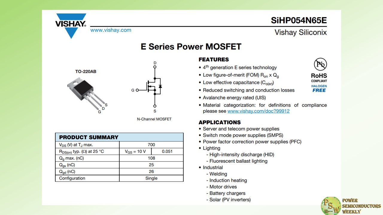
Vishay Intertechnology, Inc. introduced a new fourth-generation 650 V E Series power MOSFET that delivers high efficiency and power density for telecom, industrial, and computing applications. Compared to previous-generation devices, the Vishay Siliconix n-channel SiHP054N65E slashes on-resistance by 48.2 %, while offering a 59 % lower resistance times gate charge, a key figure of merit (FOM) for 650 V MOSFETs used in power conversion applications.
Vishay offers a broad line of MOSFET technologies that support all stages of the power conversion process, from high voltage inputs to the low voltage outputs required to power the latest high tech equipment. With the SiHP054N65E and other devices in the fourth-generation 650 V E Series family, the company is addressing the need for efficiency and power density improvements in two of the first stages of the power system architecture — power factor correction (PFC) and subsequent DC/DC converter blocks.
Typical applications will include servers, edge computing, and data storage; UPS; high intensity discharge (HID) lamps and fluorescent ballast lighting; solar inverters; welding equipment; induction heating; motor drives; and battery chargers.
Built on Vishay’s latest energy-efficient E Series superjunction technology, the SiHP054N65E’s low typical on-resistance of 0.051 Ω at 10 V results in a higher power rating for applications > 2 kW and allows the device to address the Open Compute Project’s Open Rack V3 (ORV3) standards. In addition, the MOSFET offers ultra low gate charge down to 72 nC. The resulting FOM of 3.67 Ω*nC is 1.1 % lower than the closest competing MOSFET in the same class, which translates into reduced conduction and switching losses to save energy and increase efficiency. This allows the device to address the specific titanium efficiency requirements in server power supplies or reach 96 % peak efficiency in telecom power supplies.
For improved switching performance in hard-switched topologies such as PFC, half-bridge, and two-switch forward designs, the MOSFET released today provides low typical effective output capacitances Co(er) and Co(tr) of 115 pF and 772 pF, respectively. The device’s resulting resistance times Co(er) FOM is an industry-low 5.87 Ω*pF. Offered in the TO-220AB package and providing increased dv/dt ruggedness, the SiHP054N65E is RoHS-compliant, halogen-free, and Vishay Green, and is designed to withstand overvoltage transients in avalanche mode with guaranteed limits through 100 % UIS testing.
Original – Vishay Intertechnology
-

The Volkswagen Group is reorganizing its procurement of electronic parts and semiconductors to ensure supply over the long term and, in doing so, securing itself a leading position in terms of technology as well as competitiveness. To this end, the Group has developed a new strategy for the procurement of parts with electronic components.
“A high degree of transparency in the semiconductor value chain – the exact knowledge of the parts used – enables us to better determine the global demand and availability of these components. This is underscored by risk management which, in future, will extend to the level of individual electronic parts and help us detect bottlenecks early on and avoid them.
For strategically important semiconductors and even the Group’s own planned developments in the future, we will rely on direct purchasing from the semiconductor manufacturers,” said Dirk Große-Loheide, Board Member for Procurement of Volkswagen Passenger Cars and member of Group management.
In the past, electronic components like control units were procured and the Tier 1 suppliers were largely free to decide which parts they used. Going forward, in close collaboration and partnership with Tier 1 suppliers, Group procurement will define which semiconductors and other electronic parts are to be used.
“Additionally, this is done across all brands by the Semiconductor Sourcing Committee (SSC) established especially for this purpose, with representatives from the procurement and development departments of the brands as well as from Volkswagen Group Components and CARIAD. Furthermore, the transparency regarding semiconductors means that technical alternatives can be identified and implemented more quickly in the event of bottlenecks.
Another positive effect is that a reduction in the diversity of variants in the hardware results in a lower degree of software complexity,” said Karsten Schnake, Board Member for Procurement at Škoda Auto and head of the cross-brand and cross-functional task force COMPASS (Cross Operational Management Parts & Supply Security), explaining the advantages.
Semiconductors are indispensable in the automotive industry: not only are they elementary for mass production, but they are also innovation drivers and key for launching new products on the market.
The greatest increase in demand for semiconductors is the result of the increasing electrification of vehicles and the trend towards the growing use of assistant functions through to fully autonomous driving. The corresponding innovations will also result in the use of cutting-edge semiconductors, while the demand for more common semiconductors will remain or even rise further. Vehicle innovations are heavily characterised by the use of semiconductors: in 1978, only eight semiconductors were installed in a control unit of a Porsche 911. Today, a Škoda Enyaq has around 90 control units with some 8,000 electronic components.
This development also has an impact on the value of electronic components in the vehicle, the value of which will more than double by the year 2030 from today’s average of around 600 euros per vehicle. According to the Group’s assessment and corresponding analyzes, the importance of the automotive sector as a customer of the semiconductor industry is also increasing.
Today, the automotive industry is in 5th place among the major buyers with a global procurement volume for semiconductors of around 47 billion US dollars. By 2030, our industry is expected to secure third place with a market volume of around 147 billion US dollars.
The after-effects of the COVID-19 pandemic and the associated chip crisis can still be felt. To solve these enormous challenges and ensure the semiconductor supply, the Volkswagen Group launched the COMPASS initiative at the beginning of 2022, initially with the operational focus of safeguarding the vehicle programme. Strategic action areas were identified on the basis of lessons learned during the semiconductor crisis and solutions were developed and implemented for the long term.
Original – Volkswagen
-
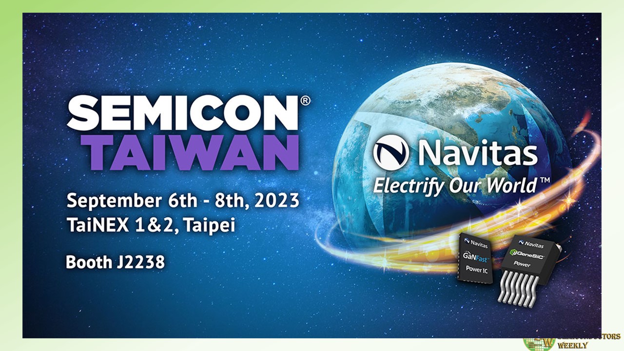
Navitas Semiconductor will reveal a new, high-performance wide bandgap power platform as part of its display at one of Asia’s most prestigious electronics exhibitions – sponsored by Navitas – SEMICON Taiwan 2023, from September 6th-8th.
Visitors will discover the latest gallium nitride (GaN) GaNFast™ power ICs integrate gallium nitride (GaN) power and drive, with control, sensing, and protection to enable faster charging, higher power density, and greater energy savings. Complementary GeneSiC™ power devices are optimized high-power, high-voltage, and high-reliability silicon carbide (SiC) solutions.
Additionally, Navitas will showcase cutting-edge, power-system platforms to dramatically accelerate customer developments, minimize time-to-market, and set new industry benchmarks in energy efficiency, power density and system cost. These system platforms include complete design collateral with fully-tested hardware, embedded software, schematics, bill-of-materials, layout, simulation and hardware test results. Examples include:
- Navitas’ CRPS185 data center power platform, that delivers a full 3,200 W of power in only 1U (40 mm) x 73.5mm x 185 mm (544 cc), achieving 5.9 W/cc, or almost 100 W/in3 power density. This is a 40% size reduction vs, the equivalent legacy silicon approach and reaches over 96.5% efficiency at 30% load, and over 96% stretching from 20% to 60% load, creating a ‘Titanium Plus’ benchmark.
- Navitas’ 6.6 kW 3-in-1 bi-directional EV on-board charger (OBC) with 3 kW DC-DC. This 96%+ efficient unit has over 50% higher power density, and with efficiency over 95%, delivers up to 16% energy savings as compared to competing solutions.
As part of SEMICON’s Power and Opto Semiconductor Forum, Navitas’ Charles Bailley, Senior Director of Business Development, will present “GaN Power ICs Increase Power Density in EV Power Systems”. The presentation is at 2pm, on September 6th, in room 402, 4F, TaiNEX 1.
“Breakthrough high efficiency, high reliability, and high power density – all from the new GaN power IC platform,” said Kevin 汪時民 Wang, Manager of Navitas Taiwan. “The new platform announcement matches SEMICON’s theme of ‘Innovating the World through Semiconductors’ and our own mission to ‘Electrify Our World™’.”
Original – Navitas Semiconductor
-
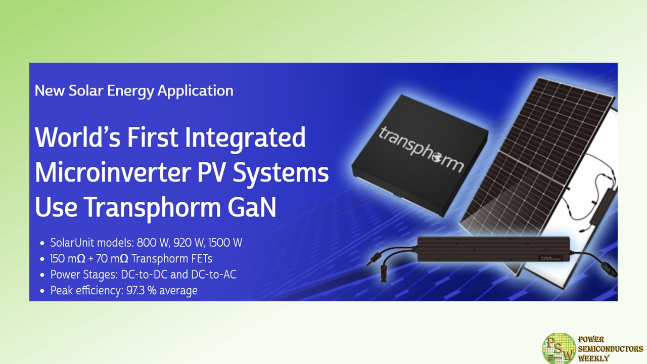
Transphorm, Inc. announced that its GaN platform powers the world’s first integrated photovoltaic (PV) systems from DAH Solar Co., Ltd. (Anhui Daheng New Energy Technology Co., LTD/subsidiary of DAH Solar). The PV systems are used in DAH Solar’s new SolarUnit product line. DAH Solar credits Transphorm’s GaN FETs with enabling it to produce smaller, lighter, and more reliable solar panel systems that also offer higher overall power generation with lower energy consumption.
The design achievements continue to demonstrate Transphorm’s One Core GaN Platform, Crossing the Power Spectrum leadership position by solidifying its value proposition in the renewables market, which currently represent a GaN TAM of more than $500M.
DAH Solar uses Transphorm’s 150 mΩ and 70 mΩ GaN FETs in the SolarUnits’ design architecture (both DC-to-DC and DC-to-AC power stages). The SolarUnits are available in three models with power outputs of 800 W, 920 W, or 1500 W and peak efficiencies of 97.16%, 97.2%, and 97.55% respectively. The GaN devices deliver higher switching frequencies and power density versus incumbent silicon solutions. Notably, the two FETs are available in PQFN88 performance packages that pair with commonly-used gate drivers—features that helped DAH Solar quicken its design time.
“We have a strong legacy of producing innovative PV products. As such, we consistently look for ways to advance our products with state-of-the-art technologies to create a better, more efficient end user experience,” said Yong Gu, GM, DAH Solar. “We view Transphorm as an authority in the field of GaN production and found their advanced GaN FETs to be the optimal devices for our new SolarUnit line. The devices are easy to design in and offer performance advantages that enable us to continue building on our legacy.”
Transphorm today supports the largest range of power conversion requirements (45 W to 10+ kW) across the widest range of power applications. The company’s FET portfolio includes 650 V and 900 V devices with 1200 V devices in development. These FETs are JEDEC and AEC-Q101 qualified, making them optimal solutions for power adapters and computer PSUs through to broad industrial UPSs and electric vehicle mobility systems.
The company’s technology innovations continue to set new benchmarks across the GaN power semiconductor industry. In parallel, they help customers bring to market new, disruptive applications in their own markets—such as DAH Solar’s PV systems.
These achievements are due to Transphorm’s normally-off SuperGaN® platform, which uses the cascode d-mode configuration to harness GaN’s intrinsic advantages. The superior physics of this high performance GaN platform design delivers competitively unmatched benefits such as easier drivability, easier designability, higher reliability, and greater manufacturability.
“The value Transphorm’s GaN platform brings to a variety of applications continues to be demonstrated by market leaders like DAH Solar,” Kenny Yim, Vice President of Asia Sales, Transphorm. “Solar inverters as well as other high-power applications require highly reliable, high performing power semiconductors that can withstand decades of operation in harsh environments.
Using Transphorm’s SuperGaN technology helps reduce power loss thereby minimizing thermal stress on other designed-in components. That’s a phenomenal achievement over alternative GaN and Silicon solutions underscoring the benefits our GaN brings to next generation power systems.”
Original – Transphorm
-
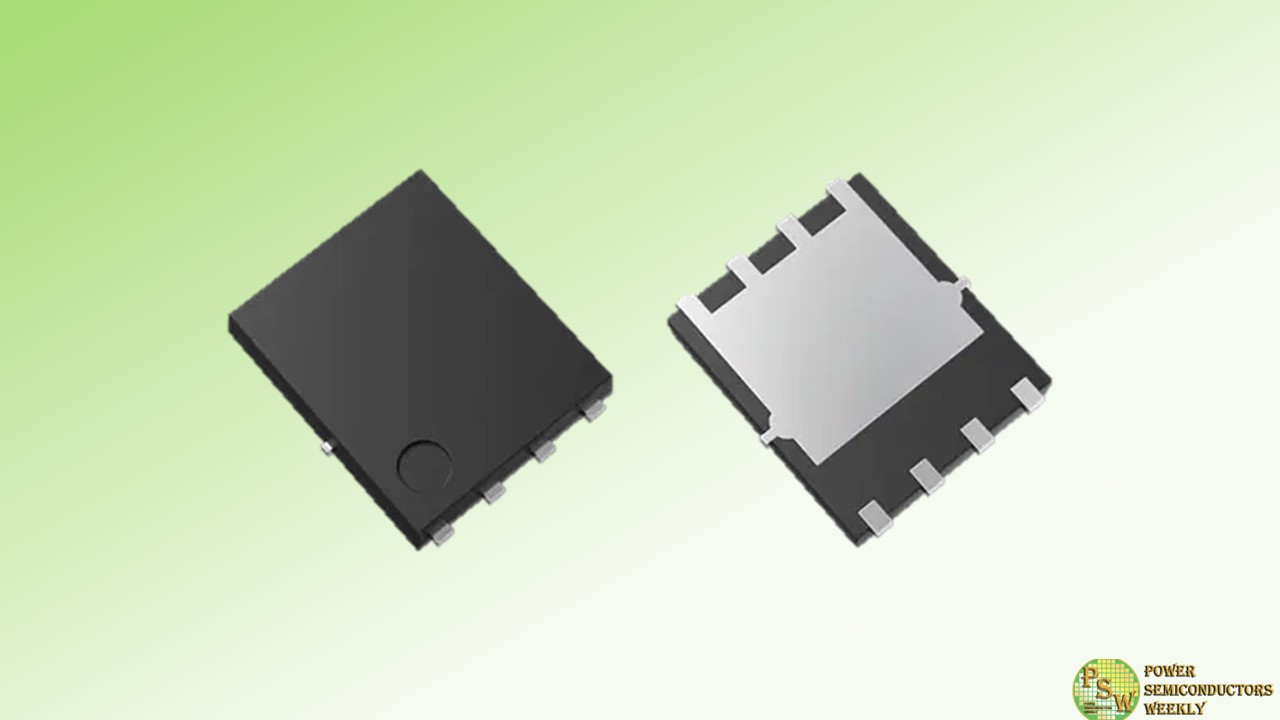
Toshiba Electronic Devices & Storage Corporation has launched three 80 V N-channel power MOSFET products that use its latest generation process “U-MOSX-H series” and are suitable for switching power supplies for industrial equipment—used for such as data centers and communication base stations—and expanded the lineup.
The new products use the surface mount type SOP Advance(N) package, and their drain-source On-resistance (max) is 3 mΩ for “TPH3R008QM”, 6 mΩ for “TPH6R008QM”, and 8.8 mΩ for “TPH8R808QM”.
The new products have reduced the figure of merits (FOMs: expressed as On-resistance × charge characteristics.) In case of TPH3R008QM, it has reduced its FOMs, drain-source On-resistance × total gate charge by approximately 48 %, drain-source On-resistance × gate switch charge by approximately 16 %, and drain-source On-resistance × output charge by approximately 33 %, compared to Toshiba’s existing product TPH4R008NH. This contributes to lowering power consumption of equipment.
Toshiba is expanding its lineup of products to help cut equipment power consumption.
Applications
- Switching power supplies (high efficiency AC-DC converters, high efficiency DC-DC converters, etc.)
- Motor control equipment (motor drives, etc.)
Features
- Latest generation process U-MOSX-H series
- Low On-resistance:
TPH3R008QM RDS(ON)=3 mΩ (max) (VGS=10 V)
TPH6R008QM RDS(ON)=6 mΩ (max) (VGS=10 V)
TPH8R808QM RDS(ON)=8.8 mΩ (max) (VGS=10 V) - High channel temperature: Tch (max)=175 °C
Original – Toshiba
