-
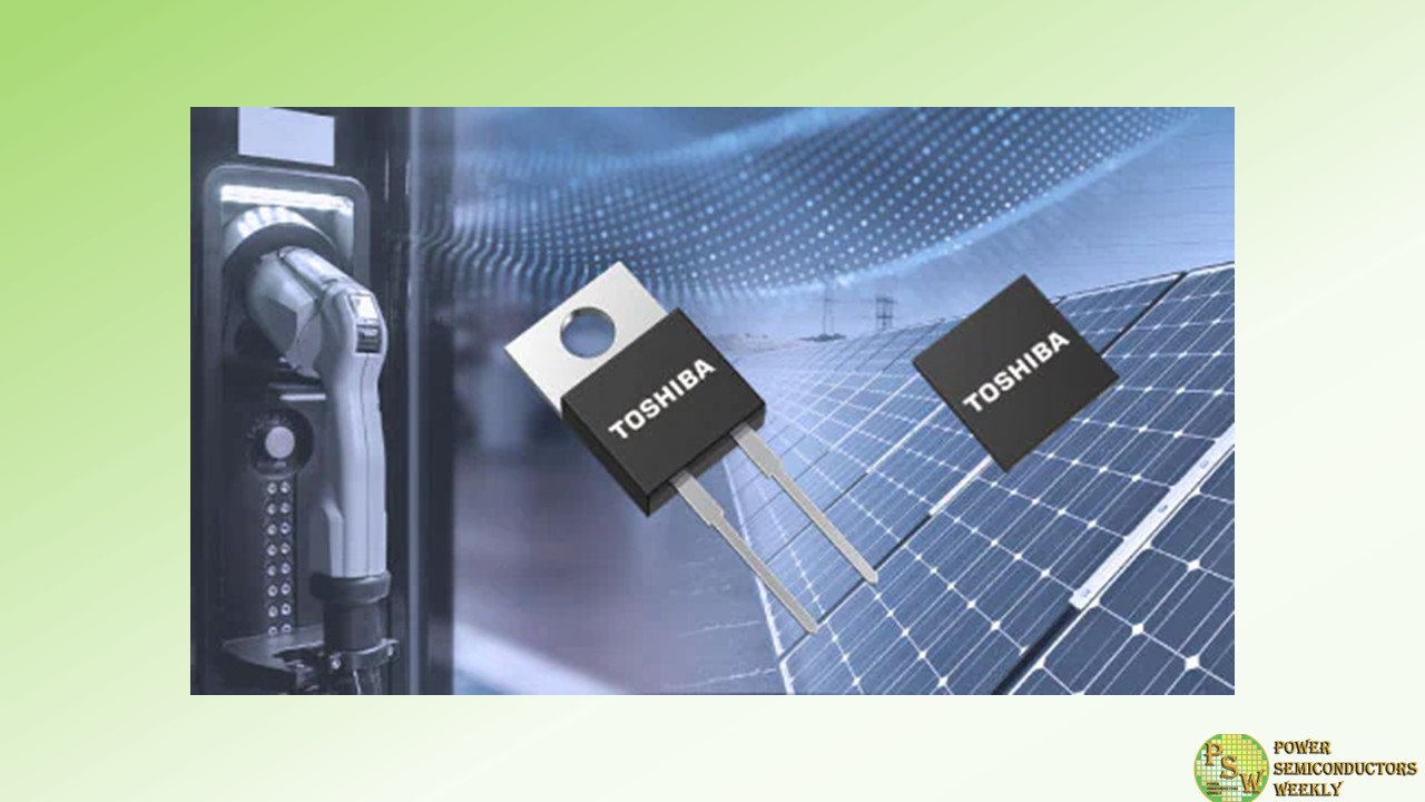
Toshiba Electronic Devices & Storage Corporation has launched the “TRSxxx65H series,” the company’s third and latest generation of silicon carbide (SiC) Schottky barrier diodes (SBDs) for industrial equipment. Volume shipments of the first 12 products, all 650V, start today, with seven products housed in TO-220-2L packages and five in DFN8×8 packages.
The new products use a new metal in a third generation SiC SBD chip that optimizes the junction barrier Schottky (JBS) structure of the second generation products. They achieve industry-leading low forward voltage of 1.2V (Typ.), 17% lower than the 1.45V (Typ.) of the previous generation.
They also improve the trade-offs between forward voltage and total capacitive charge, and between forward voltage and reverse current, which reduces power dissipation and contributes to high efficiency of equipment.
Applications
- Switching power supplies
- EV charging stations
- Photovoltaic inverters
Features
- Industry-leading low forward voltage: VF=1.2V (Typ.) (IF=IF(DC))
- Low reverse current:
TRS6E65H IR=1.1μA (Typ.) (VR=650V) - Low total capacitive charge:
TRS6E65H QC=17nC (Typ.) (VR=400V, f=1MHz)
Original – Toshiba
-
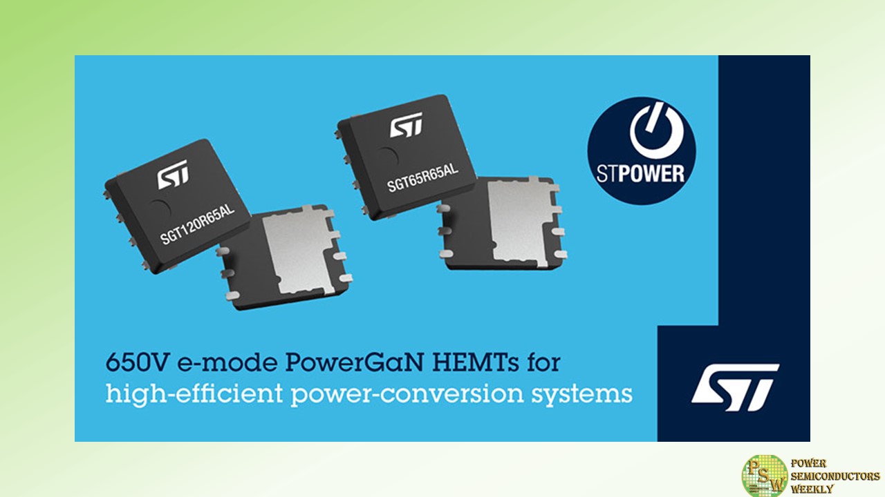
STMicroelectronics has begun volume production of e-mode PowerGaN HEMT (high-electron-mobility transistor) devices that simplify the design of high-efficiency power-conversion systems. The STPOWER™ GaN transistors raise performance in applications such as wall adapters, chargers, lighting systems, industrial power supplies, renewable energy applications, and in automotive electrification.
The first two products in the family, the SGT120R65AL and SGT65R65AL, are industrial-qualified 650V normally-off G-HEMT™ in a PowerFLAT 5×6 HV surface-mount package. They have current ratings of 15A and 25A, respectively, with typical on-resistance (RDS(on)) of 75mΩ and 49mΩ at 25°C.
Also, 3nC and 5.4nC total gate charge and low parasitic capacitances ensure minimal turn-on/turn-off energy losses. A Kelvin source connection allows optimized gate driving. In addition to the reduced size and weight of the power supplies and adapters, the two new GaN transistors provide higher efficiency, lower operating temperature, and extended life time.
In the coming months, ST will introduce new PowerGaN variants, i.e. automotive-qualified devices, as well as additional power-package options including PowerFLAT 8×8 DSC and LFPAK 12×12 for high power applications.
ST’s G-HEMT devices facilitate the transition to GaN wide-bandgap technology in power conversion. GaN transistors with the same breakdown voltage and RDS(on) as silicon alternatives can achieve lower total gate charge and parasitic capacitances, with zero reverse-recovery charge.
These properties raise efficiency and enhance switching performance, allowing higher switching frequency that permits smaller passive components thereby increasing power density. Applications can therefore become smaller with higher performance. In the future, GaN is also expected to enable new power-conversion topologies that will further improve efficiency and decrease power losses.
Original – STMicroelectronics
-

Cars with fully or partially electrified drivetrains will account for two thirds of cars produced by 2028, as per analyst forecasts. This rapid growth of electromobility is driving the demand for power semiconductors. Against this background, Infineon Technologies AG and Semikron Danfoss have signed a multi-year volume agreement for the supply of silicon-based electromobility chips.
Infineon will supply chipsets consisting of IGBTs and diodes to Semikron Danfoss. These chips are mainly used in power modules for inverters, which are used for the main drive in electric vehicles.
“As the global leader in automotive semiconductors, Infineon enables game-changing solutions for clean and safe mobility. Already today, our IGBTs and diodes play a major role in the industry’s electromobility transformation by enabling efficient power conversion in the electric powertrain,” said Peter Schiefer, President of Infineon’s Automotive division. “Our broad product portfolio, system expertise and continuous investment in our manufacturing capabilities make us a valued partner of automotive players like Semikron Danfoss.”
Claus A. Petersen, President of Semikron Danfoss added: “Semikron Danfoss provides automotive customers with power modules based on the most advanced assembly technologies that fully exploit the capabilities of IGBTs and diodes to enable further decarbonization of the transportation sector. Automotive customers trust us as an experienced long-term partner to drive the transformation in the industry.”
The IGBTs and diodes for Semikron Danfoss will be manufactured by Infineon at its sites in Dresden, Germany, and Kulim, Malaysia. Semikron Danfoss manufactures its own automotive power modules in Nuremberg and Flensburg in Germany, in Utica, US, and as of next year, in Nanjing, China.
Original – Semikron Danfoss
-

ROHM has reached a basic agreement with Solar Frontier K.K. to acquire the assets of Solar Frontier’s former Kunitomi Plant, located in Japan. The acquisition is scheduled to take place in October 2023 and will belong to the ROHM Group’s main production bases.
The role of semiconductors, one of ROHM’s core business fields is becoming increasingly important to achieving a decarbonized society.
In particular, the automotive and industrial equipment markets are undergoing technological innovation such as electrification in order to reduce environmental impact and achieve carbon neutrality. With this, the demand is increasing – especially for power and analog semiconductors.
As further expansion of the semiconductor market is expected, the ROHM Group intends to expand its production capacity continuously, particularly for silicon carbide (SiC) power devices, and ensure a stable supply to ROHM’s customers.
Original – ROHM
-

AdvanSiC has officially launched their project website. The objective of AdvanSiC is to develop, produce, test, and validate cost-effective HV SiC MOSFET semiconductors in MVDC grid applications, a full-scale wind converter, a full-scale solar inverter, and a solid-state circuit breaker for DC converter stations.
The aim is to minimize HV SiC device cost by advancing novel design structures and process optimization. Beyond this, we shall assure an immune and reliable environment to handle SiC fast transients, as well as optimize passives and cooling system to provide cost reduction not only at device level but also at system level.
The goal of AdvanSiC is to provide industrial leadership in key and emerging technologies to SMEs, start-ups, and industry from Europe to Europe, specifically in a technology that will be key to provide clean and affordable energy.
Original – AdvanSiC
-

Edgar Chen, the COO of PANJIT International Inc., will be interviewed by the chief editor of eefocus on July 11th at 15:00 at electronica China 2023. The interview will also be live-streamed online. The main focus of the interview will be on the market prospects of the semiconductor industry and the potential of PANJIT’s high-performance products in the electric vehicle, industrial control, and alternative energy sectors.
Are you curious about how PANJIT seizes opportunities and establishes a prominent presence in the automotive and industrial control markets despite the decline in consumer electronics demands? Interested in exploring PANJIT’s impressive range of high-power components like MOSFETs, IGBTs, SiC diodes, and power management ICs, along with the exciting opportunities they bring to alternative energy-related markets such as electric vehicles, charging stations, energy storage systems, and solar energy? Or perhaps you are interested in knowing about PANJIT’s key strengths and its product development strategy for the next few years?
Don’t miss the live-streamed interview on July 11th to gain valuable insights into the semiconductor industry!
Original – PANJIT International
-

Transphorm, Inc. responded to the recent news regarding China export restrictions. Late Monday, July 3, 2023, China’s Ministry of Commerce stated that it will restrict the exports of materials related to two metals used in semiconductor manufacturing: gallium and germanium. Gallium nitride (GaN) wafer materials are listed as being affected by these regulations.
Transphorm manufactures high voltage GaN power semiconductors. Trimethylgallium (TMGa) is used to produce the GaN. The company confirmed that its primary TMGa suppliers are not based in China and that suppliers have confirmed to be well-positioned to meet forecasted demand. Transphorm is therefore securely positioned to continue manufacturing and supplying its GaN devices without interruption.
Transphorm also explained gallium is generally a byproduct resulting from refinement processes used to produce popular metals such as aluminum from bauxite ore. Aluminum is produced in numerous countries such as Australia, Brazil, India, Jamaica, and the United States among others.
Transphorm will continue to the monitor the situation as necessary but sees no direct impact on its current operations. Nor does the company see long-term sourcing issues.
Original – Transphorm
-
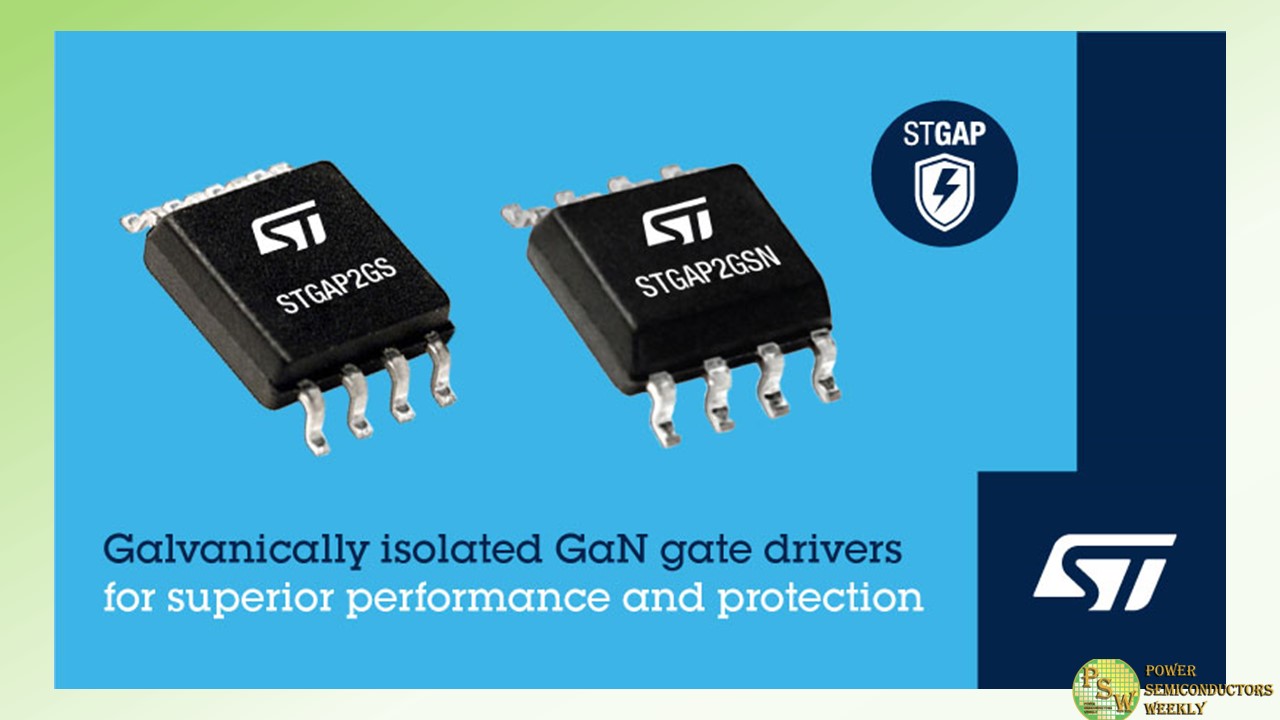
STMicroelectronics’ first galvanically isolated gate driver for gallium-nitride (GaN) transistors, the STGAP2GS, trims dimensions and bill-of-materials costs in applications that demand superior wide-bandgap efficiency with robust safety and electrical protection.
The single-channel driver can be connected to a high-voltage rail up to 1200V, or 1700V with the STGAP2GSN narrow-body version, and provides gate-driving voltage up to 15V. Capable of sinking and sourcing up to 3A gate current to the connected GaN transistor, the driver ensures tightly controlled switching transitions up to high operating frequencies.
With minimal propagation delay across the isolation barrier, at just 45ns, the STGAP2GS ensures fast dynamic response. In addition, dV/dt transient immunity of ±100V/ns over the full temperature range guards against unwanted transistor gate change. The STGAP2GS is available with separate sink and source pins for easy tuning of the gate-driving operation and performance.
Saving the need for discrete components to provide optical isolation, the STGAP2GS driver eases the adoption of efficient and robust GaN technology in various consumer and industrial applications. These include power supplies in computer servers, factory-automation equipment, motor drivers, solar and wind power systems, home appliances, domestic fans, and wireless chargers.
In addition to integrating galvanic isolation, the driver also features built-in system protection including thermal shutdown and under-voltage lockout (UVLO) optimized for GaN technology, to ensure reliability and ruggedness.
Two demonstration boards, the EVSTGAP2GS and EVSTGAP2GSN, combine the standard STGAP2GS and narrow STGAP2GSN with ST’s SGT120R65AL 75mΩ, 650V enhancement-Mode GaN transistors to help users evaluate the drivers’ capabilities.
The STGAP2GS in SO-8 widebody package, and the STGAP2GSN SO-8 narrow version, are available now, priced from $1.42 for orders of 1000 pieces.
Please visit www.st.com/stgap2gs for more information.
Original – STMicroelectronics
-
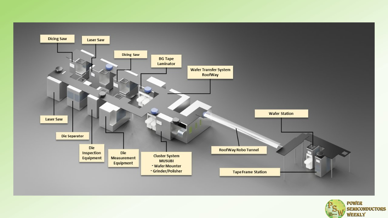
DISCO Corporation opened a new mid-process research center on July 1, 2023.
As the wafers on which circuits are built in the front-end process of semiconductor manufacturing have extremely high added-value, high yield is required in the processes that follow. Among these processes, in the grinding (wafer thinning) and dicing (wafer singulation through cutting) processes handled by DISCO, there is a risk that one processing failure may cause the entire wafer’s quality to deteriorate.
Therefore, caution and accuracy are required for operations such as processing and transfer in particular. In addition, if a large number of defects occur in the back-end process, most of the time, alternative wafers cannot immediately be supplied from the front-end process. As a result, this may have a significant impact on the entire supply chain and become a large issue in the lean manufacturing of the automotive industry.
Recognizing these issues, DISCO has newly positioned these processes that are conventionally in the back-end process of semiconductor manufacturing as part of the “mid-process,” and has been proceeding with R&D in this area.
DISCO has officially established the mid-process research center as a site to conduct R&D for the mid-process and perform demonstrations for customers. This center has permanent installations of the wafer transfer system RoofWay as well as the cluster system MUSUBI, and research is underway to reduce the equipment operator’s responsibilities and improve semiconductor wafer processing and transfer quality through automation of the production system.
As semiconductor use in automotive applications is increasing, stricter quality management is being required for semiconductors as well, as they are responsible for the user’s life. Therefore, through this center, DISCO will aim at realizing a production system that eliminates operator intervention as much as possible in order to reduce quality variation that arises from human involvement.
The mid-process research center is a facility that makes verification of unmmaned processes possible by connecting a series of processes with a fully automatic transfer robot. The processes include thinning using a grinder, singulation using dicing saws and laser saws, and pickup, inspection, and measurement of die.
The mid-process research center has been partially open since December 2021, and during the time until the official opening, DISCO has been improving the level of the system by incorporating the valuable opinions of some of the invited customers. Now, as some time has passed from when the category of COVID-19 was downgraded and reclassified as a level 5 infectious disease, DISCO felt that it was finally possible to proactively welcome visitors to the center, and thus decided to make an official announcement for the opening of the center.
Original – DISCO
-
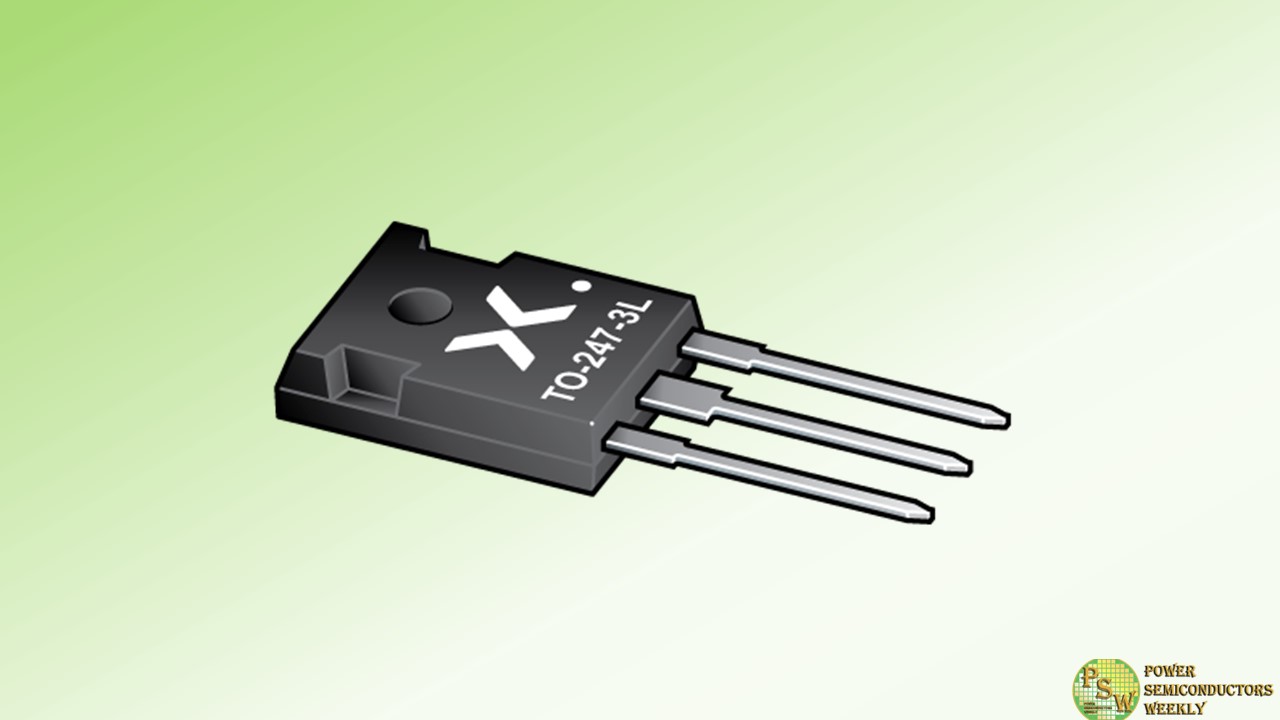
Nexperia launched its entry to the insulated gate bipolar transistor (IGBT) market with a range of 600 V devices, starting with the 30A NGW30T60M3DF. By adding IGBTs to its extensive portfolio, Nexperia is addressing the growing demand for efficient, high-voltage switching devices with a range of performance and cost requirements.
These enable higher power density in power conversion and motor drive applications, including industrial motor drives like servo motors ranging from 5 to 20 kW (20 kHz), robotics, elevators, operating grippers, in-line manufacturing, power inverters, uninterruptible power supply (UPS), photovoltaic (PV) strings, EV-charging, and induction heating and welding.
IGBT is a relatively mature technology. Nonetheless, the market for these devices is expected to grow in line with the increased adoption of solar panels and electric vehicle (EV) chargers. Nexperia’s 600 V IGBTs feature a robust, cost-effective carrier-stored trench-gate advanced field-stop (FS) construction, providing exceptionally low conduction and switching loss performance with high levels of ruggedness in operating temperatures up to 175°C. This improves the efficiency and reliability of power inverters, induction heaters, welding equipment and industrial applications like motor drives and servos, robotics, elevators, operating grippers, and in-line manufacturing.
Designers can choose between the medium speed (M3) and high speed (H3) series IGBTs. These IGBTs have been designed with very tight parameter distributions, allowing multiple devices to connect safely in parallel. In addition, lower thermal resistance than competing devices enables them to provide higher output power. These IGBTs are also fully rated as soft fast reverse-recovery diodes. This means they are suitable for rectifier and bi-directional circuit applications or to protect against overcurrent conditions.
“With the release of these IGBTs, Nexperia provides designers with a greater choice of power-switching devices for a broad range of power applications”, according to Dr. Ke Jiang, General Manager Business Group Insulated-Gate Bipolar Transistors & Modules at Nexperia. “IGBTs are the ideal complement to Nexperia’s existing range of CMOS and wide-bandgap switching devices, making Nexperia a one-stop-shop for power electronics designers.”
These IGBTs are available in a standard, lead-free, TO247-3L package and are HV-H3TRB qualified for outdoor applications. Nexperia plans to follow this release with a series of 1200 V IGBTs. To learn more about Nexperia’s IGBTs, visit: https://www.nexperia.com/igbts
Original – Nexperia
