-
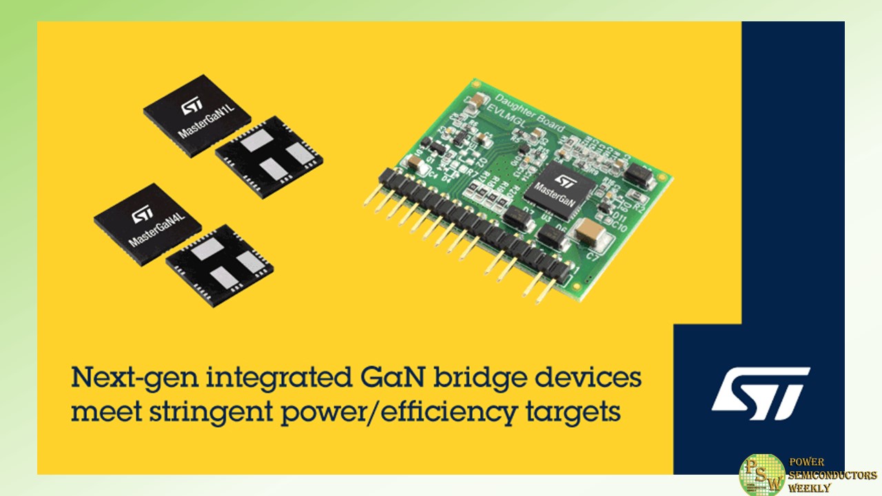
STMicroelectronics’ MasterGaN1L and MasterGaN4L introduce the next generation of integrated gallium-nitride (GaN) bridge devices that simplify power-supply design leveraging wide-bandgap technology to achieve the latest ecodesign targets.
ST’s MasterGaN family combines 650V GaN high electron-mobility transistors (HEMT) with optimized gate drivers, system protection, and an integrated bootstrap diode that helps power the device at startup. Integrating these features saves designers tackling the complex gate-drive requirements of GaN transistors. Housed in a compact power package, the devices also enhance reliability, cut the bill of materials, and ease circuit layout.
The latest devices contain two GaN HEMTs connected in half-bridge configuration. The arrangement is suitable for building switched-mode power supplies, adapters, and chargers with active-clamp flyback, active-clamp forward, and resonant converter topologies.
The MasterGaN1L and MasterGaN4L are pin compatible with MasterGaN1 and MasterGaN4 respectively. Compared to the earlier devices, they have a newly optimized turn-on delay that allows working at higher frequency and higher efficiency with low load, especially in resonant topologies.
The inputs accept signal voltages from 3.3V to 15V, with hysteresis and pull-down that facilitate connecting directly to a controlling device such as a microcontroller, DSP, or Hall-effect sensors. A dedicated shutdown pin helps designers save system power and the two GaN HEMTs have accurately matched timing with an interlocking circuit to prevent cross-conduction conditions.
The MasterGaN1L HEMTs have 150mΩ RDS(on) and 10A rated current, for use in applications up to 500W. Consuming just 20mW no-load power, and enabling high conversion efficiency, they enable designers to meet stringent industry targets for standby power and average efficiency. The MasterGaN4L HEMTs target applications up to 200W, with 225mΩ RDS(on) and rated current of 6.5A.
The EVLMG1LPBRDR1 and EVLMG4LPWRBR1 demonstration boards are available to help evaluate the features of each device. These boards contain a GaN-based half-bridge power module fine-tuned to work in an LLC application. They help quickly create new topologies leveraging the MasterGaN1L and MasterGaN4L devices without needing a complete PCB design.
Original – STMicroelectronics
-
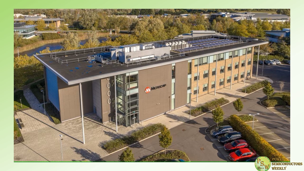
With UK and European companies seeking advanced technology to solve challenges in communications, IoT and automotive applications, many are looking for local support from major solution vendors. Microchip Technology Inc. announced the inauguration of a major new facility at Cambridge Research Park, Cambridge, UK.
At the heart of Microchip’s plans to develop more of its smart, connected and secure solutions in the UK area, the new center will add significant R&D space, which will allow Microchip’s business units to further develop their already broad offering. The new site will help Microchip improve its focus on the needs of several of its highest priority markets, such as IoT, automotive, industrial and consumer.
To gain immediate benefit from the facility, many of Microchip’s highly skilled development engineers and other staff will transfer from the company’s Ely site, with plans in hand to boost the number of employees at the Cambridge site over time.
“The Cambridge site is ideally situated in one the world’s top technology areas and will enable us to attract top talent to build state of the art products and serve our customer base,” said Sumit Mitra, senior corporate vice president of Microchip’s 32-bit microcontroller, microprocessor, wireless, aerospace and development tools business units.
“We have already onboarded a large number of talented and experienced engineers for the new center and expect that the new opportunities we will offer—to develop exciting solutions for the most significant and dynamic technology markets—will further attract the highly talented staff we need.”
“The facility is intended to become a premier Microchip engineering center, employing 200 highly skilled silicon engineering staff and advanced laboratories,” said Neel Das, senior director of Microchip’s 32-bit microcontroller business unit. “Establishing the new facility in Cambridge means we can meet this target by tapping into the wealth of engineering talent that exists in the area. The Cambridge Research Park is a hub of innovation and an excellent venue to develop the high-tech solutions on which we have built our reputation.”
The three-story building will offer approximately 10,000 square feet per floor, providing space to support multiple product lines including 16- and 32-bit microcontrollers, 32-bit microprocessors and wireless connectivity products plus technology development, physical design and human resource support.
Original – Microchip Technology
-

MACOM Technology Solutions Holdings, Inc. announced the completion of its acquisition of the radio frequency business of Wolfspeed, Inc. on December 2, 2023. The RF Business is highly complementary to MACOM’s portfolio and creates a compelling combined technology solution.
“We are excited to welcome the RF Business team to MACOM,” said Stephen G. Daly, President, Chief Executive Officer and Chair. “Going forward, we are committed to supporting all product and foundry customers and building upon the RF Business’ established technology to strengthen our leadership position.”
Original – MACOM Technology Solutions
-

DENSO Corporation announced changes to its organizational structure, executives’ responsibilities and personnel, effective January 1, 2024.
DENSO has stated at “DENSO DIALOG DAY 2023” that it will evolve from being “a Tier 1 supplier that supports the auto industry” to “a Tier 1 supplier that supports a mobility-centered society”, aiming to maximize the value of the entire mobility society, in addition to vehicles.
To achieve this, DENSO has announced its commitment to three challenges: “evolution of mobility,” “strengthening of foundational technology,” and “creating new value.” To materialize these goals, the following organizational and executive changes will be implemented.
In terms of the executive structure, two executive vice presidents will assume responsibility for the company’s major management resources in the following two areas, accelerating the formulation and execution of growth strategies. Additionally, to strengthen and expand technological development areas that will spur new growth, a Chief Innovation Officer (CIO) position will be established.
Original – DENSO
-

Axcelis Technologies, Inc. announced the grand opening of the Company’s new Axcelis Logistics Center, located at 105 Sam Fonzo Drive, Beverly, MA. The Company celebrated this milestone event with a ribbon-cutting ceremony led by President and CEO Russell Low.
The new Axcelis Logistics Center is a state-of-the-art facility designed to optimize Axcelis’ logistics and warehouse operations and provide flex capacity for the Company’s manufacturing operations to support the Company’s growth. The facility, which measures 101,800 square feet, was designed from the ground up to incorporate the latest technologies such as AI-driven autonomous mobile robots (AMRs) and other innovative enterprise-level warehouse automation to provide significant efficiency and improve material handling and flow to the Company’s operations.
The new center is designed to be energy efficient and employee friendly. It features EV charging stations, utilizes US EPA Energy Star rated heating, ventilation and air conditioning equipment and has all LED lighting with advanced motion sensors.
President and CEO Russell Low, commented, “The ribbon cutting represents the culmination of a vision ready to be set in full motion. Our investment in this new facility will allow us to support the Company’s expanding global customer base. We will continue to invest in our employees and infrastructure to ensure we have the necessary skills and capacity required to achieve our $1.3B financial model. We are also excited to provide significant employment opportunities across a wide variety of functions here in Beverly and across the globe. We look forward to continuing to play a vibrant role in our local communities and supply chain.”
The Company plans to seek a 25% tax credit under the U.S. Chips and Science Act relating to its capital investment in the new facility. The CHIPS and Science Act aims to bolster U.S. chip manufacturing to make American semiconductor supply chains more resilient and support national security and access to key technologies.
Original – Axcelis Technologies
-

Texas Instruments announced the expansion of its low-power gallium nitride (GaN) portfolio, designed to help improve power density, maximize system efficiency, and shrink the size of AC/DC consumer power electronics and industrial systems. TI’s overall portfolio of GaN field-effect transistors (FETs) with integrated gate drivers addresses common thermal design challenges, keeping adapters cooler while pushing more power in a smaller footprint.
“Today’s consumers want smaller, lighter and more portable power adapters that also provide fast, energy-efficient charging,” said Kannan Soundarapandian, general manager of High Voltage Power at TI.
“With the expansion of our portfolio, designers can bring the power-density benefits of low-power GaN technology to more applications that consumers use every day, such as mobile phone and laptop adapters, TV power-supply units, and USB wall outlets. Additionally, TI’s portfolio also addresses the growing demand for high efficiency and compact designs in industrial systems such as power tools and server auxiliary power supplies.”
The new portfolio of GaN FETs with integrated gate drivers, which includes the LMG3622, LMG3624 and LMG3626, offers the industry’s most accurate integrated current sensing. This functionality helps designers achieve maximum efficiency by eliminating the need for an external shunt resistor and reducing associated power losses by as much as 94% when compared to traditional current-sensing circuits used with discrete GaN and silicon FETs.
TI’s GaN FETs with integrated gate drivers enable faster switching speeds, which helps keep adapters from overheating. Designers can reach up to 94% system efficiency for <75-W AC/DC applications or above 95% system efficiency for >75-W AC/DC applications. The new devices help designers reduce the solution size of a typical 67-W power adapter by as much as 50% compared to silicon-based solutions.
The portfolio is also optimized for the most common topologies in AC/DC power conversion, such as quasi-resonant flyback, asymmetrical half bridge flyback, inductor-inductor-converter, totem-pole power factor correction and active clamp flyback.
To learn more about the benefits of TI GaN for the most common AC/DC topologies, read the technical article, “The benefits of low-power GaN in common AC/DC power topologies.”
TI has a long history of globally owned, regionally diverse internal manufacturing operations, including wafer fabs, assembly and test factories, and bump and probe facilities across 15 worldwide sites. TI has been investing in manufacturing GaN technology for more than 10 years.
With plans to manufacture more than 90% of its products internally by 2030, TI has the ability to provide customers with dependable capacity for decades to come.
Original – Texas Instruments
-

Nexperia announced its first silicon carbide (SiC) MOSFETs with the release of two 1200 V discrete devices in 3-pin TO-247 packaging with RDS(on) values of 40 mΩ and 80 mΩ. NSF040120L3A0 and NSF080120L3A0 are the first in a series of planned releases which will see Nexperia’s SiC MOSFET portfolio quickly expand to include devices with a variety of RDS(on) values in a choice of through-hole and surface mounted packages.
This release addresses the market demand for the increased availability of high performance SiC MOSFETs in industrial applications including electric vehicle (EV) charging piles, uninterruptible power supplies (UPS) and inverters for solar and energy storage systems (ESS).
“With these inaugural products, Nexperia and Mitsubishi Electric wanted to bring true innovation to a market that has been crying out for more wide-bandgap device suppliers”, according to Katrin Feurle, Senior Director & Head of Product Group SiC at Nexperia. “Nexperia can now offer SiC MOSFET devices which offer best-in-class performance across several parameters, including high RDS(on) temperature stability, low body diode voltage drop, tight threshold voltage specification as well as a very well-balanced gate charge ratio making the device safe against parasitic turn on. This is the opening chapter in our commitment to producing the highest quality SiC MOSFETs in our partnership with Mitsubishi Electric. Together we will undoubtedly push the boundaries of SiC device performance over the coming years”.
“Together with Nexperia, we’re thrilled to introduce these new SiC MOSFETs as the first product of our partnership”, says Toru Iwagami, Senior General Manger, Power Device Works, Semiconductor & Device Group in Mitsubishi Electric. “Mitsubishi Electric has accumulated superior expertise of SiC power semiconductors, and our devices deliver a unique balance of characteristics.”RDS(on) is a critical performance parameter for SiC MOSFETs as it impacts conduction power losses. Nexperia identified this as a limiting factor in the performance of many currently available SiC devices and used its innovative process technology to ensure its new SiC MOSFETs offer industry-leading temperature stability, with the nominal value of RDS(on) increasing by only 38% over an operating temperature range from 25°C to 175°C. Unlike other many currently available SiC devices in the market.
Nexperia’s SiC MOSFETs also exhibit the very low total gate charge (QG), which brings the advantage of lower gate drive losses. Furthermore, Nexperia balanced gate charge to have an exceptionally low ratio of QGD to QGS, a characteristic which increases device immunity against parasitic turn-on.
Together with the positive temperature coefficient of SiC MOSFETs, Nexperia’s SiC MOSFETs offers also ultra-low spread in device-to device threshold voltage, VGS(th), which allows very well-balanced current-carrying performance under static and dynamic conditions when devices are operated in parallel. Furthermore, low body diode forward voltage (VSD) is a parameter which increases device robustness and efficiency, while also relaxing the dead-time requirement for asynchronous rectification and free wheel operation.
Nexperia is also planning the future release of automotive grade MOSFETs. The NSF040120L3A0 and NSF080120L3A0 are available in production quantities now. Please contact Nexperia sales representatives for samples of the full SiC MOSFET offering.
Original – Nexperia
-
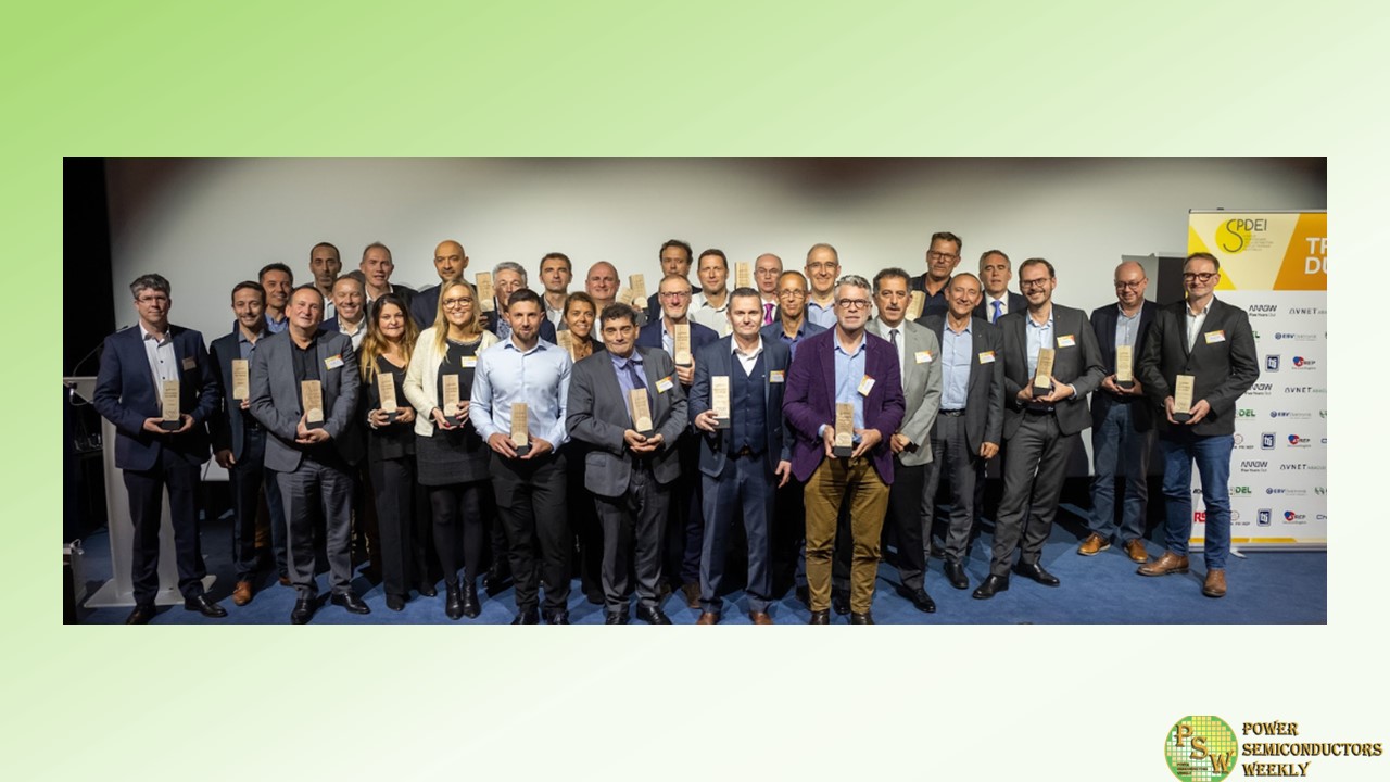
Micro Commercial Components received a supplier award in the Semiconductors/Analog category from Syndicat Professionnel de la Distribution en Electronique Industrielle (SPDEI), the French trade union for electronics distributors. Members of this powerful organization include Arrow, Silica, EBV, TTI, RS, Farnell, and others in the region.
MCC values its relationships with SPDEI distributor partners and is honored to accept this award for providing outstanding support and industry collaboration.
The 27th annual SPDEI Awards were given to a total of 27 electronics companies in the following categories:
- Semiconductors/Digital
- Semiconductors/Analog
- Wireless and Sensors
- Display and Embedded
- Passive Components
- Connectivity
- Electromechanical Components, Cables, and Accessories
- Energy
The awards ceremony was held on November 21, 2023, at the Automobile Club de France in Paris. Gilda Goltais, MCC Country Manager for France, Belgium, and North Africa, was in attendance to accept this award. MCC was one of only three companies to win in the Semiconductors/Analog category.
Prior to the awards ceremony, SPDEI held its annual conference, where key challenges, trends, and opportunities — such as French and European regulatory issues and the push for greener solutions and products — were discussed with over 100 industry professionals in attendance.
MCC would like to thank SPDEI for acknowledging the ongoing efforts to provide superior service. And MCC looks forward to supporting SPDEI members for many years to come as the power electronics industry continues to evolve.
Original – Micro Commercial Components
-

The Executive Board of Siltronic AG expects a significant improvement in sales and EBITDA by 2028. Thus, the Group sales are expected to exceed EUR 2.2 billion by 2028 and the EBITDA margin to reach the high 30’s per-centage area. Based on the Group sales forecast for 2023, this corresponds to an increase in sales of more than 40 percent. The EBITDA margin will also improve significantly compared to the 28 to 30 percent forecast for 2023. The targets are based on stable overall price and exchange rate developments (EUR/USD: 1.10).
For the upcoming year 2024, Siltronic expects that at least the first half of the year will still be bur-dened by high inventories at chip manufacturers and their customers. On the earnings side, the start-up costs of the new production site in Singapore will have a negative impact on the company’s margin in 2024.
The confidence until 2028 is supported by the increasing relevance of global megatrends such as artificial intelligence, digitalization and electromobility. This will lead to a strong increase in demand for semiconductors and therefore also for wafers. For example, the wafer area required to manu-facture an AI-compatible server is up to eight times larger than that required for a conventional server. The wafer area required for electric vehicles is also 60 to 100 percent higher than for con-ventional combustion vehicles.
The increase in Group profitability will mainly be driven by the expected volume growth and higher cost efficiency, which will be significantly higher than the expected inflation-related cost increases.
Above-average growth in Siltronic’s focus activities
The company expects wafer demand to grow by an average of four to five percent per year until at least 2028 and a positive trend in all segments: Memory, Logic and Power. Growth is expected to be particularly strong for 300 mm wafers, especially in the leading edge area, as well as for wafers for Power applications. Siltronic should be able to benefit from these trends in particular thanks to its good market positions.
The company has made systematic preparations for the expected growth phase with high investments, especially for the construction of a new production fab for 300 mm wafers in Singapore (FabNext) and the improvement of the product mix in Freiberg, Saxony. At the beginning of November 2023, the first wafers were produced in Singapore – slightly earlier than planned. Production will be gradually ramped from the beginning of 2024. In view of the high level of automation and efficient cost structure, Siltronic is aiming for EBITDA margins of more than 50 percent for FabNext in the mid-term.
Siltronic is already characterized by a high level of resilience, which is reflected in its consistently solid margins even in difficult economic times. In addition to its high cost sensitivity, this is primarily due to its close customer relationships. The company has entered into long-term agreements with many of its customers, securing around two thirds of its sales.
“In view of the expected next growth phase driven by megatrends, we have defined medium-term targets for Siltronic up to 2028 against which we will be measured. Group sales are expected to increase to more than EUR 2.2 billion and the EBITDA margin to the high 30’s. Among other things, we will benefit from our new, highly efficient fab in Singapore, our technological leading position and our strength in the Power segment,” commented Dr. Michael Heckmeier, CEO of Siltronic AG, on the development.
Future use of capital focused on securing further growth opportunities, strengthening tech-nology leadership and reducing debt
Siltronic will make investments of around EUR 1.3 billion for the above-mentioned projects in 2023. However, as of September 30, 2023, the company maintains a robust financial position with an eq-uity ratio of 49 percent and holds in excess of EUR 500 million in cash and cash equivalents, along with financial assets.
This reflects a sound and secure financial and balance sheet structure. After reaching the peak of investment activity in 2023, expenditures are expected to noticeably decrease again by more than 50 percent in 2024 alone compared to the previous year. Siltronic will consist-ently invest the cash flows generated in the course of the planned targets in securing organic growth opportunities, expanding automation and digitalization, strengthening its leading technology position and further improving the quality of its balance sheet, including reducing debt.
This also includes a continued strong focus on research and development (R&D) in order to continue to utilize technology-driven competitive advantages in the future. In the medium term, between four and five percent of Group sales are to be invested in R&D activities.
“Despite the peak of our investments in 2023, we are in a very solid position with an equity ratio of almost 50 percent and a high liquidity reserve. From 2024, our capex will fall noticeably, but organic growth with the expansion of FabNext remains our top priority. In addition, we will use the expected cash flows from our growth plan until 2028 to strengthen our leading technology position and im-prove the quality of our balance sheet. This will create sustainable value for all our stakeholders,” adds Claudia Schmitt, CFO of Siltronic AG.
Original – Siltronic
-
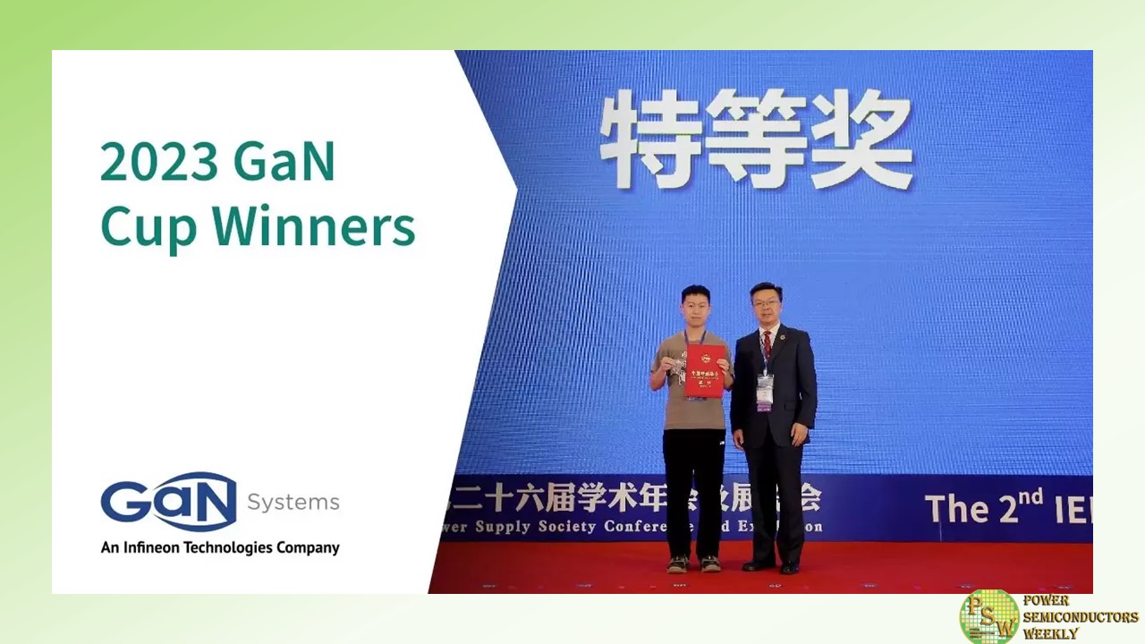
GaN Systems™, an Infineon Technologies Company, announced the winners for the 9th “GaN Systems Cup” Power Electronics Application Design Competition at the 2023 China Power Electronics and Energy Conversion Congress and the 26th China Power Supply Society Annual Conference & Exhibition (CPEEC & CPSSC 2023), taking place on November 10-13, 2023, in Guangzhou, China. The Xi’an Jiaotong University team’s three-phase inverter prototype design was recognized as the Grand Prize for achieving outstanding efficiency and power density with GaN Systems’ high-performance power transistors.
Since 2015, the Power Electronics Application Design Competition has encouraged over a thousand college students to sharpen their knowledge with practical design experience and explore possibilities in power electronics.
Participation was again unprecedented this year, with 68 teams from 48 top universities submitting project proposals. Out of the 24 teams that entered finals, 10 eventually received recognition. The Xi’an Jiaotong University team earned the Grand Prizes for their outstanding high-efficiency, high-power density three-phase inverter design. With an output power of 500W, an input voltage of 350VDC, and an output voltage of 220VAC with frequency increased from 50Hz to 400Hz and eventually 2000Hz, the team’s design delivered an impressive 15W/in3 power density and average 98% efficiency.
“The power industry is constantly looking for novel approaches to create more powerful, smaller, and faster components that increase overall system power density and efficiency,” said Yunsheng Qu, Senior Manager of Infineon’s Power and Sensor Systems Division, at the award ceremony. “GaN adoption is now at the tipping point in many applications, and developing a pipeline of skilled, talented engineers has become ever-crucial to support such massive market growth potential. I am pleased to see many of the winning entries not only meet the design requirements but go well beyond them.”
Co-located with the GaN Systems Cup, CPEEC & CPSSC 2023 drew a record-breaking 2,600 visitors and nearly 100 exhibitors, making it China’s largest academic event in power electronics. Infineon’s GaN Systems business line showcased an array of groundbreaking power system reference designs for automotive, industrial, and consumer applications. The impressively compact and economical 11kW 800V GaN-based onboard charger reference design was the main attraction in the booth. Visitors also showed a high level of interest in the implementation benefits enabled by the new Gen4 platform and responded positively to the closing of the Infineon acquisition.
Original – GaN Systems
