-

Wolfspeed, Inc. announced the expansion of an existing long-term silicon carbide wafer supply agreement with a leading global semiconductor company. The expanded agreement, which is now worth approximately $275 million in total, calls for Wolfspeed to supply the company with 150mm silicon carbide bare and epitaxial wafers, reinforcing both companies’ visions for an industry-wide transition from silicon to silicon carbide semiconductor power devices.
“As the global leader in silicon carbide wafer production, Wolfspeed is uniquely positioned to be a critical supplier of high-quality and advanced silicon carbide materials at scale. We will continue to be an important partner to power device manufacturers who need the highest-quality silicon carbide wafers to service their customers,” said Dr. Cengiz Balkas, SVP and GM of Materials for Wolfspeed.
“This agreement further strengthens our long-time partnership with a best-in-class power semiconductor manufacturer. Our collective efforts are helping to address the rapidly expanding opportunity for silicon carbide and better address the unfulfilled demand that exists in the marketplace today.”
The adoption of silicon carbide-based power solutions is rapidly growing across multiple markets, including industrial and EVs. Silicon carbide solutions enable smaller, lighter and more cost-effective designs, converting energy more efficiently to unlock new applications in electrification. This supply agreement will enable silicon carbide applications in a broad range of industries, such as: renewable energy and storage, electric vehicles, charging infrastructure, industrial power supplies, traction and variable speed drives.
Wolfspeed is the global leader in the manufacturing of silicon carbide wafers and epitaxial wafers. The company is currently expanding its manufacturing capacity in the United States and has plans to open a new, automated materials factory in Siler City, North Carolina later this year that will produce 200mm silicon carbide wafers. The new materials factory will increase Wolfspeed’s current materials production capacity by ten times.
Original – Wolfspeed
-

JEDEC Solid State Technology Association announced the publication of JEP198: Guideline for Reverse Bias Reliability Evaluation Procedures for Gallium Nitride Power Conversion Devices. Developed by JEDEC’s JC-70.1 Gallium Nitride Subcommittee, JEP198 is available for free download from the JEDEC website.
JEP198 presents guidelines for evaluating the Time Dependent Breakdown (TDB) reliability of GaN power transistors. It is applicable to planar enhancement-mode, depletion-mode, GaN integrated power solutions, and cascode GaN power transistors.
This publication covers suggested stress conditions and related test parameters for evaluating the TDB reliability of GaN power transistors using the off-state bias. The stress conditions and test parameters for both High Temperature Reverse Bias Stress and Application Specific Stress-Testing are designed to evaluate the reliability of GaN transistors over their useful lifetime under accelerated stress conditions.
“We are becoming more dependent on power electronics in all facets of our daily lives. As such, the technologies behind those systems are advancing and so too must the device-specific qualification processes. The new GaN-focused Guideline for Reverse Bias Reliability Evaluation is a critical step toward achieving that goal,” said Ron Barr, VP of Quality and Reliability, Transphorm and Co-Chair of the Task Group 701_1.
“This was a collaborative effort conducted by both GaN semiconductor and end product manufacturers. I’m proud of the work the task group delivered. It is an important framework to ensure cross-industry uniformity that will, in the end, provide power system manufacturers the necessary confidence when designing with GaN devices.”
“With the rise of renewable energy and electrification of our lives, the efficiency of power semiconductors is becoming more critical. This is where GaN power semiconductors have proven to be a valuable technology. The Guideline for Reverse Bias Reliability Evaluation is another step in improving confidence in GaN Technology and the products that are on and being brought to market,” said Dr. Kurt Smith, VP of Reliability and Qualification at VisIC Technologies and Chair of JC-70.1.
“This document was developed through collaboration of the multi-corporation team of industry experts to represent the best practices for evaluating GaN devices. It was a long multi-year process to reach consensus and the team is to be commended for the quality document and all of the hard work that went into it.”
Original – JEDEC
-

MIT and Applied Materials, Inc. announced an agreement today that, together with a grant to MIT from the Northeast Microelectronics Coalition (NEMC) Hub, commits more than $40 million of estimated private and public investment to add advanced nano-fabrication equipment and capabilities to MIT.nano, the Institute’s center for nanoscale science and engineering.
The collaboration will create a unique open-access site in the United States that supports research and development at industry-compatible scale using the same equipment found in high-volume production fabs to accelerate advances in silicon and compound semiconductors, power electronics, optical computing, analog devices and other critical technologies.
The equipment and related funding and in-kind support provided by Applied Materials will significantly enhance MIT.nano’s existing capabilities to fabricate up to 200mm (8-inch) wafers, a size essential to industry prototyping and production of semiconductors used in a broad range of markets including consumer electronics, automotive, industrial automation, clean energy and more. Positioned to fill the gap between academic experimentation and commercialization, the equipment will help establish a bridge connecting early-stage innovation to industry pathways to the marketplace.
“A brilliant new concept for a chip won’t have impact in the world unless companies can make millions of copies of it. MIT.nano’s collaboration with Applied Materials will create a critical open-access capacity to help innovations travel from lab bench to industry foundries for manufacturing,” said Maria Zuber, MIT’s Vice President for Research and E. A. Griswold Professor of Geophysics. “I am grateful to Applied Materials for its investment in this vision. The impact of the new toolset will ripple across MIT and throughout Massachusetts, the region, and the nation.”
Applied Materials is the world’s largest supplier of equipment for manufacturing semiconductors, displays and other advanced electronics. The company will provide at MIT.nano several state-of-the-art process tools capable of supporting 150 and 200mm wafers and will enhance and upgrade an existing tool owned by MIT. In addition to assisting MIT.nano in the day-to-day operation and maintenance of the equipment, Applied engineers will develop new process capabilities which will benefit researchers and students from MIT and beyond.
“Chips are becoming increasingly complex, and there is tremendous need for continued advancements in 200mm devices, particularly compound semiconductors like silicon carbide and gallium nitride,” said Aninda Moitra, Corporate Vice President and General Manager of Applied Materials’ ICAPS Business. “Applied is excited to team with MIT.nano to create a unique, open-access site in the U.S. where the chip ecosystem can collaborate to accelerate innovation. Our engagement with MIT expands Applied’s university innovation network and furthers our efforts to reduce the time and cost of commercializing new technologies while strengthening the pipeline of future semiconductor industry talent.”
The Northeast Microelectronics Coalition (NEMC) Hub, managed by the Massachusetts Technology Collaborative (MassTech), will allocate $7.7 million to enable the installation of the tools. The NEMC is the regional “hub” that connects and amplifies the capabilities of diverse organizations from across New England plus New Jersey and New York. The U.S. Department of Defense (DoD) selected the NEMC Hub as one of eight Microelectronics Commons Hubs and awarded funding from the CHIPS and Science Act to accelerate the transition of critical microelectronics technologies from lab-to-fab, spur new jobs, expand workforce training opportunities and invest in the region’s advanced manufacturing and technology sectors.
The Microelectronics Commons program is managed at the federal level by the Office of the Under Secretary of Defense for Research and Engineering (OUSD(R&E)) and the Naval Surface Warfare Center, Crane Division, and facilitated through the National Security Technology Accelerator (NSTXL), which organizes the execution of the eight regional hubs located across the country. The announcement of the public sector support for the project was made at an event attended by leaders from the DoD and NSTXL during a site visit to meet with NEMC Hub members.
“The installation and operation of these tools at MIT.nano will have a direct impact on the members of the NEMC Hub, the Massachusetts and Northeast regional economy, and national security. This is what the CHIPS and Science Act is all about,” said Ben Linville-Engler, Deputy Director at the MassTech Collaborative and the interim director of the NEMC Hub. “This is an essential investment by the NEMC Hub to meet the mission of the Microelectronics Commons.”
MIT.nano is a 200,000 square-foot facility located in the heart of the MIT campus with pristine, class-100 cleanrooms capable of accepting these advanced tools. Its open-access model means that MIT.nano’s toolsets and laboratories are available not only to the campus but also to early-stage R&D by researchers from other academic institutions, non-profit organizations, government and companies ranging from Fortune 500 multinationals to local startups. Vladimir Bulović, faculty director of MIT.nano, said he expects the new equipment to come online in early 2025.
“With vital funding for installation from NEMC and after a thorough and productive planning process with Applied Materials, MIT.nano is ready to install this toolset and integrate it into our expansive capabilities that serve over 1,100 researchers from academia, startups, and established companies,” said Bulović, who is also the Fariborz Maseeh Professor of Emerging Technologies in MIT’s Department of Electrical Engineering and Computer Science (EECS). “We’re eager to add these powerful new capabilities and excited for the new ideas, collaborations, and innovations that will follow.”
As part of its arrangement with MIT.nano, Applied Materials will join the MIT.nano Consortium, an industry program comprising 12 companies from different industries around the world. With the contributions of the company’s technical staff, Applied Materials will also have the opportunity to engage with MIT’s intellectual centers, including continued membership with the Microsystems Technology Laboratories (MTL).
Original – Applied Materials
-

Power Integrations announced the release of the InnoSwitch™5-Pro family of high-efficiency, programmable flyback switcher ICs. The single-chip switcher achieves over 95 percent efficiency with a novel secondary-side control scheme which achieves zero-voltage switching (ZVS) without a dedicated and costly additional high voltage switch.
The new IC, which features a 750 V or a 900 V PowiGaN™ primary switch, primary-side controller, FluxLink™ isolated feedback and secondary controller with an I2C interface, optimizes the design and manufacture of compact, highly efficient single- or multi-port USB PD adapters. Applications are notebooks, high-end cellphones and other portable consumer products, including designs that require the new USB PD EPR (Extended Power Range) protocol.
Adnaan Lokhandwala, senior product marketing manager at Power Integrations said: “The combination of ZVS and GaN is power supply magic. Switching losses vanish, and we can leverage the low conduction losses of GaN to implement super dense adapter layouts with far fewer components than asymmetric half-bridge (AHB) circuits or active clamp alternatives. For example, we have demonstrated 140 W / 28 V USB PD adapters in 4.2 cubic inches using only 106 components. The flyback topology used by InnoSwitch5-Pro ICs is much easier to implement than AHB and can also operate from universal mains with or without a PFC stage.”
InnoSwitch5-Pro flyback switcher ICs feature lossless input line voltage sensing on the secondary side for adaptive DCM/CCM and ZVS control to maximize efficiency and simplify design across line and load. The ICs also feature a post-production tolerance offset to facilitate accurate output constant-current (CC) control of better than two percent to support the UFCS protocol.
Excellent efficiency – better than 95 percent – allows designers to eliminate heat sinks, spreaders and potting materials for thermal management, further reducing size, weight, component cost and manufacturing complexity. Key markets for the InnoSwitch5-Pro family of flyback switcher ICs include high-density USB PD 3.1 Extended Power Range (EPR), UFCS and multi-protocol adapters, notebook adapters and after-market single- and multi-port chargers and adapters.
Original – Power Integrations
-

TTI, Inc. announced that the company is now an authorized distributor of PANJIT semiconductors. TTI is excited to now stock PANJIT’s high performance semiconductor products, giving electronics designers access to a wider range of components to suit their needs.
“We are excited to embark on a global partnership agreement with PANJIT which will further strengthen our portfolio of discrete components, bringing a leading range of diodes, MOSFETs, protection devices, Bipolar Junction Transistors, SiC devices, and ICs to our customers across many industrial and transportation applications,” said John Drabik, President TTI Americas.
“PANJIT’s vision is to power the world with our reliable and energy-efficient products, bringing people a greener and smarter future,” says Edgar Chen, COO at PANJIT. “It is a great honor to partner with TTI globally as we unite to expand the reach of our innovative discrete and IC products to a wider audience.”
TTI is committed to delivering the right part at the right time to its customers. The introduction of PANJIT products to TTI’s portfolio means designers now have access to a wider selection of semiconductor products, all available from one source, so they can find the perfect parts for their application.
PANJIT has built an enviable reputation for manufacturing reliable semiconductor components, including MOSFET, Schottky, ESD , Diodes, TVS, SiC devices, bipolar junction transistors, bridges, , Fast Recovery Diodes, and ICs, which are ideal for markets such as industrial, automotive, power management and communication & networking.
Original – PANJIT International
-
Abstract
A novel 4H-SiC trench metal-oxide-semiconductor field-effect transistor (TMOS) with depletion-mode pMOS (D-pMOS) is proposed and investigated via TCAD simulation. It has an auxiliary gate electrode that controls the electrical connections of P-shield layers under the trench bottom through the D-pMOS. In linear operation, the D-pMOS is turned off and then the potential of the P-shield layers is raised with the auxiliary gate, which shrinks the width of the depletion region of the P-shield/N-drift junction to reduce the resistance of the JFET region. In the saturation operation, the saturation current density of the proposed TMOS is reduced, benefiting from its relatively large cell pitch.
The design concept eases the tension between specific on-resistance and short circuit capabilities. Numerical simulation results show that the proposed TMOS exhibits a short circuit withstand time that is 1.92 times longer than that of the conventional TMOS. In addition, a drive tactic is introduced and optimized for the proposed TMOS, which requires only one set of gate drivers. Compared with the conventional TMOS, the switching performance is improved and the switching loss is reduced by 40%.
1. Introduction
Silicon carbide (SiC) metal-oxide-semiconductor field-effect transistors (MOSFETs) with higher critical breakdown fields, lower switching loss, and better thermal conductivity are of interest to replace silicon-insulated gate bipolar transistors (Si IGBTs) in power electronic applications. This is particularly true for the electric vehicle (EV) industry today, where the range anxiety of driving an EV is the primary motivation for developing high-power-density and high-efficiency power systems. Starting with the milestone of the first SiC UMOSFET introduced by Cree Research, significant improvements in on-state resistance and power density have been achieved with the transition from the planar gate to trench gate.
The fatal weakness of SiC trench-gate MOSFETs (TMOS) is a crowded electric field at the trench corner, which causes premature breakdown. The oxide electric field at the trench corner (ECorner) is recommended to be less than 4 MV/cm. To date, designs to suppress the ECorner have been extensively studied. In addition, some structures have been developed and commercialized, such as Rohm’s double-trench MOSFET and Infineon’s asymmetric-trench MOSFET. The introduction of the grounded P-shield regions under the trench bottom is an effective approach to suppress the electric field at the trench corners, but the specific on-resistance (RON, sp) is sacrificed due to the increase in the resistance of the junction field-effect transistor (RJFET).
Y. Wang proposed an optimized UMOSFET with low RON, sp, by introducing an additional N-type layer under the grounded P-shield regions to attenuate RJFET. J. Wei proposed a novel MOSFET structure featuring both trench and planar channels, which increased the channel density and thus improved the trade-off relationship between RON, sp, and ECorner. M. Zhang proposed a new SiC trench MOSFET structure with self-biased p-shield, using an external self-biasing network, which reduces RJFET and keeps a low off-state oxide field. Based on that, Y. Xing introduced a depletion P-channel MOS (D-pMOS) to the conventional TMOS. The new structure adjusts the potential of the P-shield via the D-pMOS for low on-state resistance.
Nevertheless, the saturation current density of TMOS also increases with increasing channel density and decreasing on-state resistance, which means that the short-circuit (SC) capability of TMOS is even weaker and the SC withstanding time (tSC) is shorter. T. Yang proposed an embedded JFET structure inside TMOS to reduce the peak SC current. W. Ni reported the optimization of the overlap region of the grounded P-shield layers to improve the trade-off relationship between RON, sp, and tSC. The major challenge, however, is to improve the trade-off relationship between RON, sp and SC capabilities in the development of SiC TMOS.
In this article, a new design of 4H-SiC TMOS with depletion-mode pMOS (D-pMOS) is proposed and studied via Silvaco TCAD simulation. A D-pMOS is embedded into SiC MOSFET and an auxiliary gate electrode is introduced to control the electrical connections of P-shield layers under the trench bottom. The design concept significantly improves the trade-off relationship between RON, sp and SC capability. In addition, a drive method for the proposed TMOS is introduced to achieve lower switching loss.
The subsequent sections of the paper are organized as follows. Section 2 introduces the device structure and design concept of the proposed TMOS. Section 3 presents the numerical simulation results and discussion, while Section 4 provides the conclusion.
2. Device Structure and Design Concept
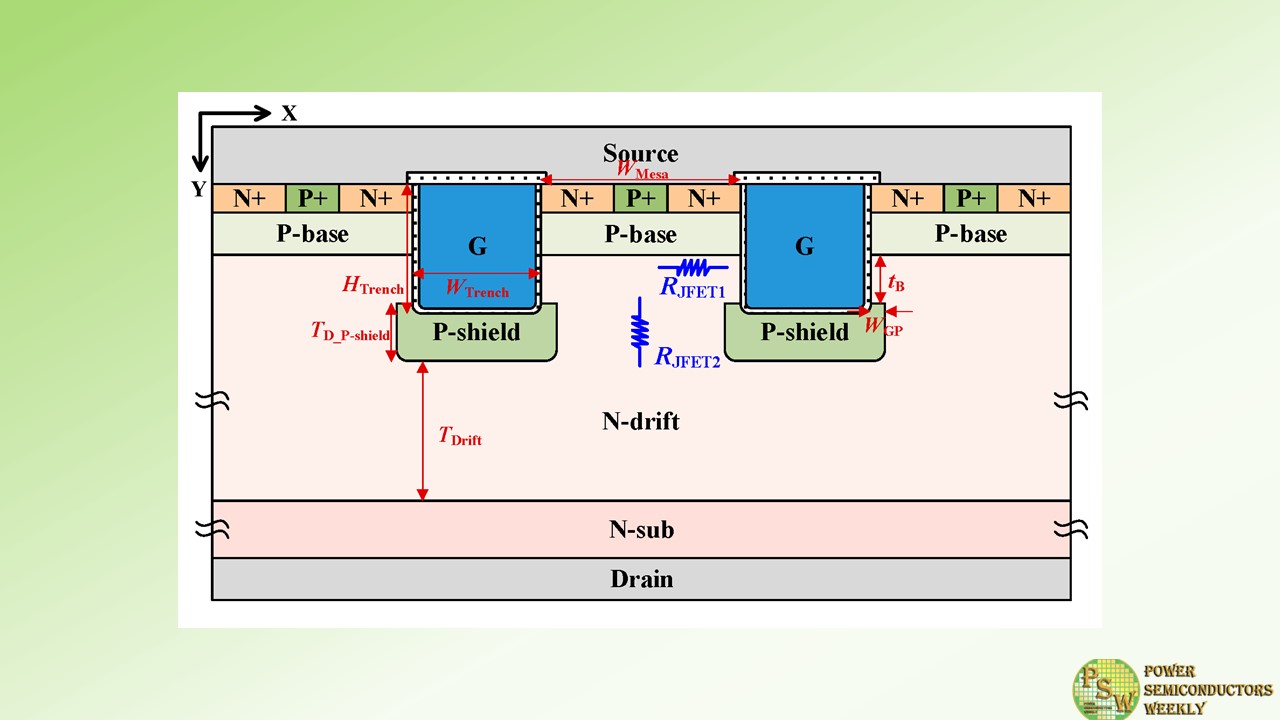
Figure 1 shows the cross-sectional views of the conventional trench MOSFET with grounded P-shield layers (GP-TMOS) and the proposed TMOS with D-pMOS. The proposed TMOS is derived from the GP-TMOS, but it has two unique structural features.
To create a depletion-mode pMOS, a lightly doped P-type layer is positioned between the P+ layer and the P-shield layer. In addition, the poly-Si gate is split into two parts, called the main gate (MG) and the auxiliary gate (AG). The MG controls the n-MOS, while the AG controls the D-pMOS. The two device structures share the device parameters as those listed in Table 1.
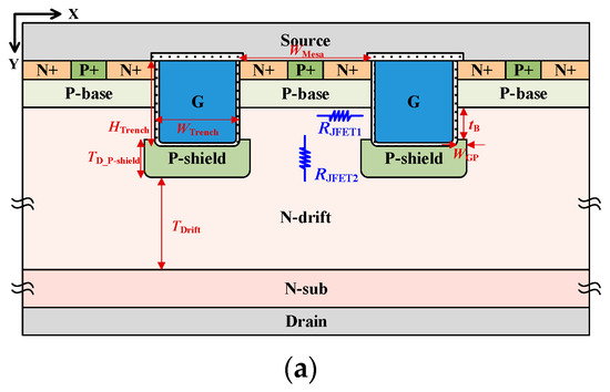
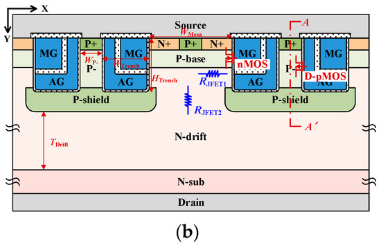
Figure 1. Cross-sectional views of (a) the conventional GP-TMOS, and (b) the proposed TMOS.
Table 1. Device parameters for TCAD simulations.
The RJFET of the GP-TMOS consists of two parts, as shown in Figure 1a. RJFET1 is formed between the P-base and P-shield, and RJFET2 is formed between adjacent P-shield layers. They can be expressed as

Here, WGP is the horizontal distance of the P-shield layer beyond the gate trench. WD_P-shield is the depletion region width of the P-shield/N-drift junction. WD_P-base is the depletion region width of the P-base/N-drift junction. tB is the vertical distance between P-base and P-shield. TP-shield is the thickness of the P-shield layer. VD is the potential of the P-shield/N-drift junction. According to Equation (3), the P-shield layer potential VD determines the extent of the depletion region in the JFET region of TMOS.
In the forward on-state, the P-shield layer of the proposed TMOS is disconnected from the source electrode by turning off the D-pMOS, and its potential is affected and increased by the voltage of the AG. Figure 2 shows the current density distributions for the GP-TMOS and the proposed TMOS at VMG = 18 V and VAG = 18 V. In the linear operation (Vds = 1 V), the depletion region width (WD) of the P-shield/N-drift junction for the proposed TMOS is smaller than that of the GP-TMOS, as illustrated in Figure 2a,b.
The current path width of the proposed TMOS is widened to decrease RJFET. In the saturation operation (Vds = 800 V), WD for the proposed TMOS is the same as that of the GP-TMOS, as well as the current path width in a single-cell pitch, as shown in Figure 2c,d. This indicates that RJFET1 and RJFET2 of the proposed TMOS are equal to those of the GP-TMOS in a single-cell pitch. Due to a relatively large cell pitch, the saturation current (Jsat) of the proposed TMOS can be remarkably reduced for the same active area. Thus, the proposed TMOS achieves a superior tradeoff relationship between RON, sp and SC capability.
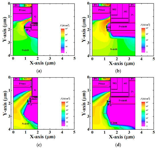
Figure 2. Current density distributions of two devices. (a) GP-TMOS at Vds = 1 V; (b) the proposed TMOS at Vds = 1 V; (c) GP-TMOS at Vds = 800 V and (d) the proposed TMOS at Vds = 800 V.
Figure 3a depicts the energy band diagram of the sandwiched P-type layers along the cutline A-A’ (shown in Figure 1b). When VAG = 0 V, the hole barrier between the P+ layer and the P-shield layer is small. The lightly doped P- layer can transport holes from the P-shield to P+, as shown in Figure 3b, indicating that the P-shield layer is grounded.
When VAG = 18 V, the EV from the P-shield layer to the P- layer decreases, resulting in a hole barrier. This is because the lightly doped P-layer is completely depleted, preventing holes’ transportation from the P-shield layer to the P+ layer, as shown in Figure 3c. This means that the P-shield layer is disconnected from the source electrode and is floating.
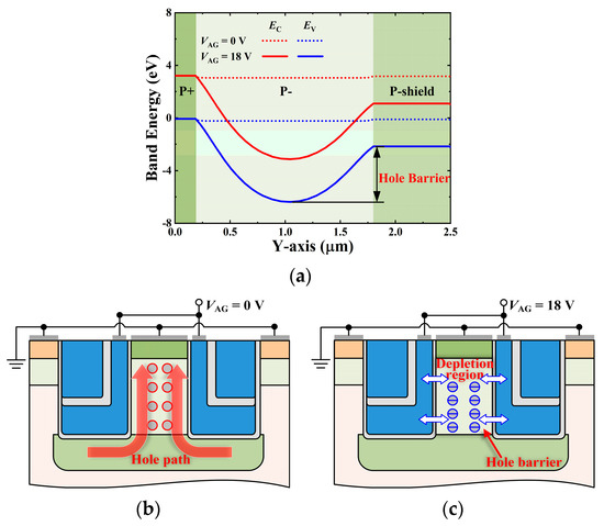
Figure 3. (a) Energy band diagram of the sandwiched P-type layers along the cutline A-A’, and operation mechanisms at (b) VAG = 0 V and (c) VAG =18 V.
In the blocking voltage state, the P-shield layer of the proposed TMOS is connected to the source electrode by turning on the D-pMOS, similar to that of the GP-TMOS. The grounded P-shield layer protects the gate oxide from the high electric field, and then maintains a reliable blocking high voltage capability.
During the switching transient, the P-shield layer of the proposed TMOS is also connected to the source electrode for safe operation. This is because the TMOS with floating P-shield layers has a notorious drawback, which is called dynamic on-resistance degradation. The proposed TMOS has an additional gate electrode, but only one set of gate drivers is required, as shown in Figure 4a.
Using two gate drive resistances, RAG-g and RMG-g, nMOS and D-pMOS can operate asynchronously. Figure 4b shows the waveforms of the MG voltage and AG voltage. The D-pMOS is set to turn off after the nMOS has turned on, keeping the P-shield layer grounded during the switching transient for reliable dynamic operation.
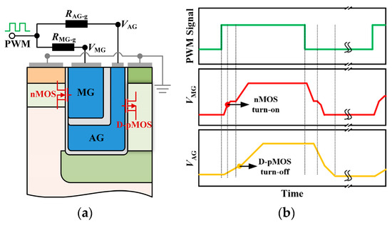
Figure 4. (a) Simplified diagram of the gate driver principle; (b) waveforms of two gate voltages.
3. Simulation Results and Discussion
The physical models include recombination models, incomplete ionization models, mobility models, bandgap narrowing models, and impact ionization models. It is noted that the Giga module is employed to capture self-heating effects and thermoelectric powers. The channel mobility of the TMOS is fixed to 50 cm2/V·s. In this comparison, the numerical simulation parameters are identical.
Figure 5 shows the impact of the width, WP-, and the doping concentration of the lightly doped P- layer, NP-, on the RON, sp (VMG = 18 V, VAG = 18 V and Jds = 200 A/cm2) and Jsat (VMG = 18 V, VAG = 18 V and Vds = 800 V) values of the proposed TMOS. As WP- and NP- decrease, RON, sp decreases and then remains at a fixed value. This is because the electrical connection state of the P-shield layer changes from grounded to floating. A small WP- and a low NP- facilitate the depletion of the P- layer. In contrast, Jsat increases as WP- and NP- decrease. The maximum Jsat is still below 6.5 kV/cm2 due to the relatively large cell pitch for the proposed TMOS.
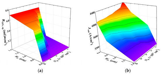
Figure 5. Impact of WP- and NP- on (a) RON, sp and (b) Jsat for the proposed TMOS.
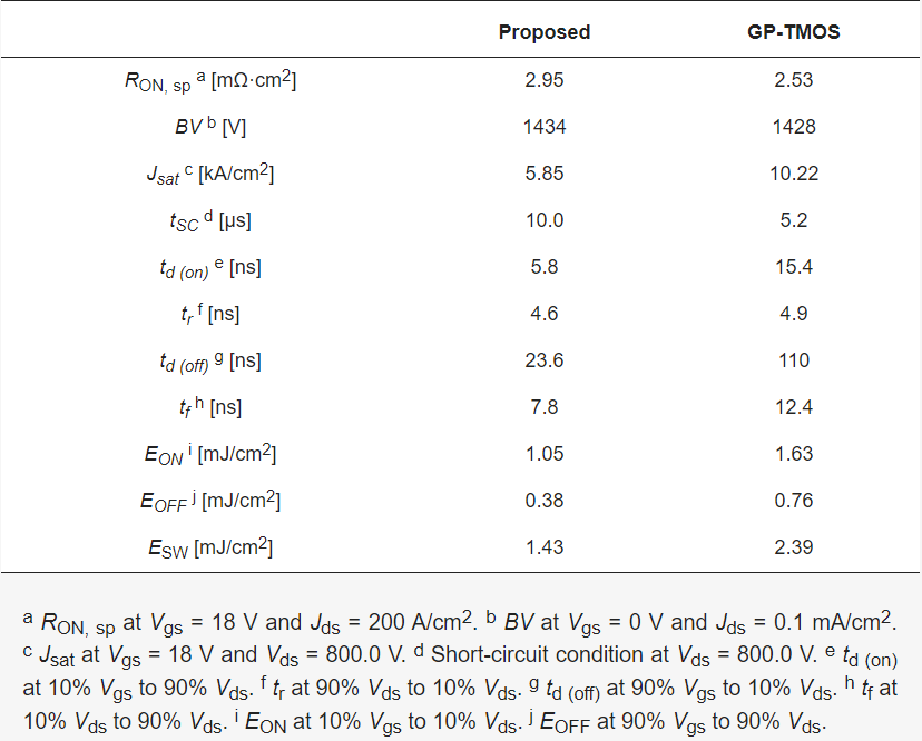
Figure 6 shows the forward output characteristics for the proposed TMOS and the GP-TMOS. The WP- and NP- of the proposed TMOS are 1.0 μm and 4.0 × 1016 cm−3. The RON, sp of the proposed TMOS and the GP-TMOS is 2.95 mΩ·cm2 and 2.53 mΩ·cm2 with Vgs = 18 V and Jds = 200 A/cm2, respectively. The RON, sp of the proposed TMOS is approximately 10% higher than that of the GP-TMOS, whereas the Jsat of the proposed TMOS is substantially reduced from 10.22 kA/cm2 to 5.85 kA/cm2, a reduction of nearly 43%.
Figure 7 shows the blocking voltage characteristics. The P-shield layer of the proposed TMOS is grounded (VMG = 0 V and VAG = 0 V). The blocking behavior of the proposed TMOS is similar to that of the GP-TMOS. The maximum electric field of both is located at the P-shield/N-drift junction.
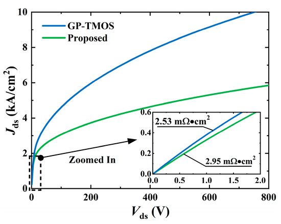
Figure 6. The output characteristics of the proposed TMOS and the GP-TMOS.
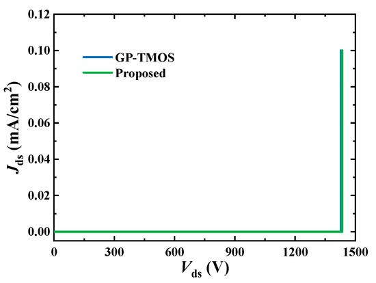
Figure 7. The blocking characteristics of the proposed TMOS and the GP-TMOS.
Figure 8 displays the SC-simulated waveforms of the current density, Jds, and the temperature profile for both the proposed TMOS and the GP-TMOS with Vgs = 18 V and Vds = 800.0 V. The peak current density of the proposed TMOS is decreased by 30%. Therefore, the junction temperature of the proposed TMOS is also lower, which could postpone the triggering of thermal runaway. Compared to the GP-TMOS, the SC withstanding time (tSC) of the proposed TMOS increases from 5.2 μs to 10.0 μs, which is approximately 1.92 times longer. The new design concept significantly eases the tension between RON, sp and tSC.
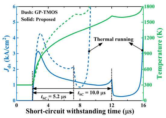
Figure 8. Short-circuit waveforms of the proposed TMOS and the GP-TMOS.
Figure 9 shows the schematic diagram of the dynamic switching simulation. The switching voltage and current are set to 800.0 V and 20.0 A, respectively. The stray inductance in the power loop is 5 nH. Figure 10 shows the influences of the AG resistance, RAG-g, and the doping concentration of the P-layer, NP-, on the power loss of the proposed TMOS. The power loss includes turn on loss and turn off loss. The RMG-g is set to 5, 10, and 20 Ω, and the dependence relationships are shown in Figure 10a–c. As NP- and RAG-g increase, the power loss decreases for various RMG-g.
This is caused by the change in the P-shield layer’s connection state during the switching transient, from a floating state to a grounded state. The TMOS with floating P-shield layers has poor dynamic performance and exhibits relatively higher switching loss. As NP- increases, a relatively high AG voltage is required to fully deplete the P-layer, which affects the threshold voltage of the D-pMOS. On the other hand, increasing RAG-g delays the triggering of the D-pMOS’s turn off during the turn on stage of the proposed TMOS. Both of the above methods can achieve grounded P-shield layers during the switching on transient of the proposed TMOS.
Figure 11 shows the switching waveforms of the proposed TMOS under two conditions. Condition I is NP- = 1 × 1016 cm−3 and RAG-g = 1 Ω, while condition II is NP- = 4 × 1016 cm−3 and RAG-g = 20 Ω. Under condition I, the D-pMOS turns off before the nMOS turns on. The turn on behavior of the proposed TMOS is the same as that of the TMOS with floating P-shield layers, where the expanding depletion region of the P-shield/N-drift junction cannot shrink back immediately, resulting in a slower switching speed and dynamic RON degradation. Under condition II, the D-pMOS turns off after the nMOS turns on. The switching performance is obviously improved by grounding the P-shield.
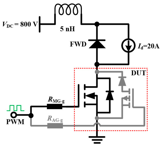
Figure 9. The schematic diagram of the dynamic switching simulation.
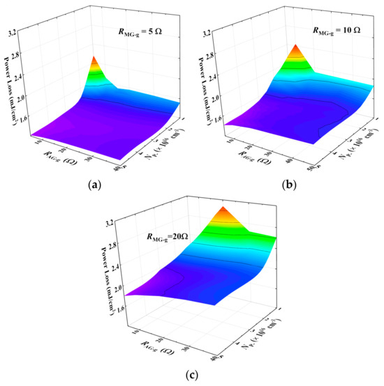
Figure 10. Influences of RAG-g and NP- on the power loss, when (a) RMG-g = 5 Ω, (b) RMG-g = 10 Ω, and (c) RMG-g = 20 Ω.
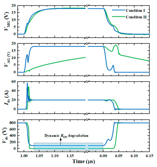
Figure 11. Switching waveforms of the proposed TMOS for condition I (NP- = 1 × 1016 cm−3, RAG-g = 1 Ω) and condition II (NP- = 4 × 1016 cm−3, RAG-g = 20 Ω).
Figure 12 compares the switching waveforms for the proposed TMOS and the GP-TMOS. Both the gate resistance of the GP-TMOS and the MG resistance of the proposed TMOS are set to 10 Ω. The NP- and RAG-g of the proposed TMOS are 4.0 × 1016 cm−3 and 5 Ω, respectively. The optimized AG resistance ensures a reliable switching operation without dynamic RON degradation. Moreover, the switching speed of the proposed TMOS is improved, due to the split-gate structure.
The proposed TMOS exhibits a shorter switching time as a result of its lower gate drain capacitance. The tON and tOFF of the SFP-SG-MOSFET are both smaller than those of the GP-TMOS and decrease by 48.7% and 74%, respectively. The switching power losses are calculated as shown in Figure 13. The turn on loss (EON) for the proposed TMOS is 1.05 mJ/cm2, which is reduced by about 35.5% compared to the GP-TMOS. The turn off loss (EOFF) for the proposed TMOS is 0.38 mJ/cm2, which is reduced by about 50% compared to that of the GP-TMOS.
The total switching loss (ESW) for the proposed TMOS is as low as 1.43 mJ/cm2, showing a 40% reduction compared to that of the GP-TMOS. The performance comparison of the two devices is offered in Table 2.
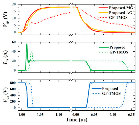
Figure 12. Switching waveforms of the proposed TMOS and the GP-TMOS.
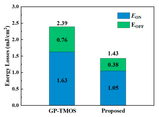
Figure 13. Switching losses of the proposed TMOS and the GP-TMOS.
Table 2. Comparison of two structure device characteristics.
4. Conclusions
A novel 4H-SiC-trench MOSFET with a depletion-mode pMOS (D-pMOS) is proposed and investigated numerically. Using the D-pMOS, the potential of the P-shield layer of the proposed TMOS can be controlled using an auxiliary gate. The width of the depletion region of the P-shield/N-drift junction is adaptively modulated in the linear and saturation operating regions.
Consequently, the proposed TMOS acquires a superior RON, sp—tSC tradeoff, achieving a 92% longer short-circuit withstanding time than that of the GP-TMOS. Moreover, the proposed TMOS flexibly utilizes two different gate resistances, while using only one set of gate drivers, which suppresses the dynamic RON degradation and further reduces switching loss. It achieves a 40% lower switching loss than that of the GP-TMOS. The superior SC capability and lower switching dissipation of the proposed TMOS hold the promise of enhancing the efficiency and reliability of power electronic systems.
Authors
Hengyu Yu, Limeng Shi, Monikuntala Bhattacharya, Michael Jin, Jiashu Qian, Anant K. Agarwal
Original – MDPI
-

PANJIT introduced new P-channel and N-channel MOSFETs designed to boost automotive electronic systems. The P-channel MOSFETs, with AEC-Q101 qualification and a high 175°C junction temperature, offer optimal choices for design engineers seeking reliability and simplified circuitry. These MOSFETs, minimizing RDS(ON) and maximizing avalanche ruggedness, are available in flexible packages (DFN3333-8L, DFN5060-8L, DFN5060B-8L, TO-252AA, TO-263, and TO-263-7L).
PANJIT’s N-channel power MOSFETs employ advanced trench technology, delivering excellent figure of merit (FOM), lower RDS(ON), and capacitance. Available in low-profile packages (DFN3333-8L, DFN5060-8L, DFN5060B-8L, TO-252AA), these MOSFETs contribute to efficient and reliable PCB layouts.
By combining innovation with reliability, PANJIT’s low voltage MOSFETs simplify power design circuitry, addressing the evolving needs of automotive design engineers.These components are a testament to PANJIT’s commitment to shaping the future of automotive electronics, offering optimal solutions for high-performance automotive applications.
Key Features of 30V & 40V Automotive-Grade P-Channel MOSFET:
• P-channel enhancement mode logic level MOSFETs
• Low RDS(ON) to minimize conduction losses
• Package with low thermal resistance
• 100% unclamped inductive switching (UIS) tested
• Electrostatic sensitive device (ESD) capable
• AEC-Q101 qualified and PPAP capable
• 175°C operating junction temperature
• Available in TO-263-7L PackageKey Features of 30V & 40V Automotive-Grade N-Channel MOSFET:
• 30V & 40V N-channel advanced trench
• Low RDS(ON) to minimize conduction losses
• Low FOM to minimize driver losses
• Standard and logic level available
• AEC-Q101 qualified and PPAP capable
• 175°C operating junction temperatureOriginal – PANJIT International
-

Navitas Semiconductor invites visitors to experience “Planet Navitas” and collaborate to “Electrify Our World” at APEC 2024 (Long Beach, CA, February 26th-29th, 2024).
Since its inception in 1985, the Applied Power Electronics Conference (APEC) has become the world’s premier event in power electronics, with high-caliber, peer-reviewed technical content from industry and academia. The APEC 2016 keynote by Dan Kinzer, COO / CTO and co-founder, was the public debut for start-up Navitas and GaNFast power ICs.
Following the mission to “Electrify our World™”, the “Planet Navitas” exhibition booth invites visitors to discover how next-gen GaN and SiC technology enable the latest solutions for fully-electrified housing, transportation and industry. Examples range from TV power to home-appliance motors and compressors, EV charging, solar/micro-grid installations, and on to data center power systems. Each example highlights end-user benefits, such as increased portability, longer range, faster charging, and grid-independence, plus a focus on how low-carbon-footprint GaN and SiC technology can save over 6 Gtons/yr CO2 by 2050.
“APEC is a significant event in the power industry calendar, with an intense schedule of customer discussions on new technologies and systems,” said Mr. Kinzer. “Complementary GaNFast™ and GeneSiC™ portfolios, with comprehensive, application-specific system design support accelerates customer time-to-market with sustainable performance advantages. ‘Planet Navitas’ represents the very real, inspiring implementation of GaN & SiC across the vast $22B/year market opportunity.”
Major technology updates and releases include GaNSafe – the world’s most-protected, most-reliable and highest-performance GaN power, Gen-4 GaNSense Half-Bridge ICs – the most integrated GaN devices, Gen-3 Fast SiC power FETs – for high-power performance, and breakthrough bi-directional GaN for game-changing motor drive and energy-storage applications.
APEC 2024 will take place at the Long Beach Convention & Entertainment Center, 300 East Ocean Boulevard, Long Beach, CA 90802, with exhibition running from February 26th – 28th. “Planet Navitas” is featured at booth #1353.
Technical presentations:
- Tuesday 27th February
- “Reducing System Cost with GaN HEMTs in Motor Drive Applications”
- 8:55am, IS05.2, Alfred Hesener, Sr. Dir. Industrial & Consumer
- 10:40am, PSTT02.6, Bin Li, Dir. Applications
- 11:40am, PSTT01.9, Xiucheng Huang, Sr. Director
- 3:45pm, exhibitor presentation, location: 101B
- “Reducing System Cost with GaN HEMTs in Motor Drive Applications”
- Thursday 29th February
- “SiC & Package Innovations in Power Modules”
- 8:30am-11:20am, IS19, Stephen Oliver, Session Chair.
- 8:55am, PSTIS21.2, Tom Ribarich, Sr Dir. Strategic Marketing
- 1:30pm-3:10pm, IS27, Llew-Vaughan-Edmunds, Session Chair
- 2:20pm, IS27-3, Stephen Oliver, VP Corp Mktg & IR, and Llew Vaughan-Edmunds, Sr Dir. GeneSiC
- “SiC & Package Innovations in Power Modules”
Student Job Fair:
- From Los Angeles to Shanghai, careers at Navitas span cutting-edge IC design and innovative applications engineering to pioneering research and ensuring customer success and revenue growth. Meet the experts and join the team!
- Tuesday, February 27, 1:30pm-5pm, Regency Ballroom ABC of the Hyatt Regency hotel, right next to the Long Beach Convention Center, with Shaun Sandera, Sr. Human Resources Manager
To schedule a meeting with the Navitas team, email info@navitassemi.com, or select from the bookings calendars below:
Customer (Private Room): https://bit.ly/navitas-apec-24-customer-private-room
Customer Meeting (On-Booth): https://bit.ly/navitas-apec-24-customer-on-boothOriginal – Navitas Semiconductor
- Tuesday 27th February
-

Moov, the largest and fastest-growing global marketplace for used semiconductor equipment, announced the release of its new Equipment Management Software (EMS) for semiconductor manufacturers. Moov’s Equipment Management Software helps manufacturers track and understand what equipment assets they own across fabrication centers (fabs), the condition of these tools, and the resale value of these assets based on data from Moov’s global marketplace.
Today, semiconductor manufacturers have limited insight into the equipment they own across fabs, its condition, and how to maximize its value once it is considered depreciated and/or has outlived its initial production line.
In building EMS, Moov will continue to help manufacturers operationalize a more data-driven approach to deciding how to leverage idle or underutilized capital equipment – whether that means transferring equipment between fabs, scrapping equipment, selling parts, or selling whole systems to maximize the lifetime value of these assets.
“Semiconductor manufacturers have neither the tools nor the data to make informed decisions on what to do with capital equipment assets that may be depreciated on their books but still have real market value,” said Moov cofounder and CEO, Steven Zhou.
“Moov’s Equipment Management Software helps manufacturers gain a unified view of their equipment across fabs and augments equipment data with marketplace data pulling from millions of data points on pricing, supply, demand, geography, installed base, and more to help chipmakers make strategic decisions on how to maximize the value of these financial assets based on true market conditions.”
To help manufacturers simplify the process of deploying EMS across fabs, Moov is offering free equipment audits and data onboarding. Moov will audit and inspect tools across a manufacturer’s fabs, and document tool make, model, location, condition, and specifications in the EMS. Once a manufacturer’s assets are tracked in the EMS, the system will automatically pull in data on pricing and demand from Moov’s global marketplace for used semiconductor manufacturing equipment.
Manufacturers can then leverage this holistic view of their assets, which are indexed and easily searchable across locations, to decide what to do with underutilized equipment and parts. If manufacturers decide to sell assets, they can easily do so in 2-clicks through a direct integration with Moov’s global resale marketplace.
“We’re taking all of the legwork out of implementing a holistic system for tracking semiconductor manufacturing equipment across fabs, in order to empower manufacturers to reduce waste and redundancies, more quickly respond to shifting needs from fab to fab, and maximize the value of assets that may have hitherto been considered a write-off but have substantial market value,” said Zhou.
Historically, what to do with depreciated equipment has been considered an afterthought by chipmakers as the process of reselling equipment was onerous and fragmented, and the resale value of equipment low. However, equipment delays and shortages of the pandemic era, the rising demand for 200mm capacity, and changing procurement habits of manufacturers to diversify their capital equipment supply chains, have led to a surge in the resale value of semiconductor manufacturing equipment.
At the same time, increased market pressures to improve both the financial and environmental sustainability of fabs has created the need for a better approach to maximizing the value of these 6-figure+ assets throughout their lifecycle.
“With access to the world’s largest data set for the resale value of semiconductor manufacturing equipment, we felt it was our responsibility to build technology to help manufacturers better incorporate this data into their day-to-day decision-making process,” said Zhou.
Original – Moov
-

Infineon Technologies AG announced a partnership with Shenzhen based Sinexcel Electric Co., Ltd., a global leader in core power equipment and solutions for the Energy Internet. Infineon will provide Sinexcel with its industry-leading 1200 V CoolSiC™ MOSFET power semiconductor devices in combination with EiceDRIVER™ compact 1200 V single-channel isolated gate drive ICs to further improve the efficiency of energy storage systems.
Driven by the carbon peaking and carbon neutrality strategy and the new energy wave, the domestic energy storage market has maintained sustained and rapid development in recent years. According to the Chinese Ministry of Industry and Information Technology, in the first half of 2023, the newly installed capacity of energy storage reached 8.63 GWh, equivalent to the total installed capacity of previous years.
The efficiency and power density of energy storage systems are important factors of product competitiveness, while the size, weight and cost of energy storage systems are closely related to the energy conversion efficiency and directly affect the product cost. Therefore, power semiconductor components play a crucial role.
“The SiC power solution is an important component for future green energy production and storage applications. Infineon’s cooperation with Sinexcel in the field of energy storage inverters enables energy storage systems to achieve advantages such as high efficiency, small size, and light weight, providing a solid guarantee for high-reliability and high-performance energy storage systems,” said Mr. Yu Daihui, Senior Vice President of Infineon Technologies and Head of Green Industrial Power Division in Greater China.
“By using Infineon’s SiC devices, Sinexcel’s energy storage products are obviously more compact and flexible, with significantly higher efficiency and lower losses, which reduces the heat dissipation cost of systems, is conducive to the long-term efficient and stable operation of products, and helps end users improve their operational stability and shorten their return on investment cycle.
This greatly improves the system competitiveness of our products and enhances the trust of clients in our energy storage products and the brand awareness of Sinexcel. We hope that in the future, Infineon will further provide high-performance and high-stability components to help enhance the competitiveness of Sinexcel’s products on the client side,” said Mr.Wei Xiaoliang, Deputy General Manager of Sinexcel.
With more than 20 years of product development and application experience in the SiC field, Infineon has been working nonstop to develop more sophisticated SiC products. Due to their high power density, Infineon’s 1200 V CoolSiC MOSFETs can reduce losses by 50 percent and provide ~2 percent additional energy without increasing the battery size, which is especially beneficial for high-performance, lightweight and compact energy storage solutions.
By using Infineon’s 1200 V CoolSiC MOSFETs and EiceDRIVER compact 1200 V single-channel isolated gate drive ICs, Sinexcel’s energy storage converters achieve high power density, minimum electromagnetic radiation and interference, high protection performance and high reliability. This allows a system efficiency of up to 98 percent, which is 1 percent higher than that of traditional solutions, reaching the industry-leading level and better meeting the needs of on-grid and off-grid energy storage applications in both domestic and overseas markets.
Original – Infineon Technologies
