
Abstract
A novel 4H-SiC trench metal-oxide-semiconductor field-effect transistor (TMOS) with depletion-mode pMOS (D-pMOS) is proposed and investigated via TCAD simulation. It has an auxiliary gate electrode that controls the electrical connections of P-shield layers under the trench bottom through the D-pMOS. In linear operation, the D-pMOS is turned off and then the potential of the P-shield layers is raised with the auxiliary gate, which shrinks the width of the depletion region of the P-shield/N-drift junction to reduce the resistance of the JFET region. In the saturation operation, the saturation current density of the proposed TMOS is reduced, benefiting from its relatively large cell pitch.
The design concept eases the tension between specific on-resistance and short circuit capabilities. Numerical simulation results show that the proposed TMOS exhibits a short circuit withstand time that is 1.92 times longer than that of the conventional TMOS. In addition, a drive tactic is introduced and optimized for the proposed TMOS, which requires only one set of gate drivers. Compared with the conventional TMOS, the switching performance is improved and the switching loss is reduced by 40%.
1. Introduction
Silicon carbide (SiC) metal-oxide-semiconductor field-effect transistors (MOSFETs) with higher critical breakdown fields, lower switching loss, and better thermal conductivity are of interest to replace silicon-insulated gate bipolar transistors (Si IGBTs) in power electronic applications. This is particularly true for the electric vehicle (EV) industry today, where the range anxiety of driving an EV is the primary motivation for developing high-power-density and high-efficiency power systems. Starting with the milestone of the first SiC UMOSFET introduced by Cree Research, significant improvements in on-state resistance and power density have been achieved with the transition from the planar gate to trench gate.
The fatal weakness of SiC trench-gate MOSFETs (TMOS) is a crowded electric field at the trench corner, which causes premature breakdown. The oxide electric field at the trench corner (ECorner) is recommended to be less than 4 MV/cm. To date, designs to suppress the ECorner have been extensively studied. In addition, some structures have been developed and commercialized, such as Rohm’s double-trench MOSFET and Infineon’s asymmetric-trench MOSFET. The introduction of the grounded P-shield regions under the trench bottom is an effective approach to suppress the electric field at the trench corners, but the specific on-resistance (RON, sp) is sacrificed due to the increase in the resistance of the junction field-effect transistor (RJFET).
Y. Wang proposed an optimized UMOSFET with low RON, sp, by introducing an additional N-type layer under the grounded P-shield regions to attenuate RJFET. J. Wei proposed a novel MOSFET structure featuring both trench and planar channels, which increased the channel density and thus improved the trade-off relationship between RON, sp, and ECorner. M. Zhang proposed a new SiC trench MOSFET structure with self-biased p-shield, using an external self-biasing network, which reduces RJFET and keeps a low off-state oxide field. Based on that, Y. Xing introduced a depletion P-channel MOS (D-pMOS) to the conventional TMOS. The new structure adjusts the potential of the P-shield via the D-pMOS for low on-state resistance.
Nevertheless, the saturation current density of TMOS also increases with increasing channel density and decreasing on-state resistance, which means that the short-circuit (SC) capability of TMOS is even weaker and the SC withstanding time (tSC) is shorter. T. Yang proposed an embedded JFET structure inside TMOS to reduce the peak SC current. W. Ni reported the optimization of the overlap region of the grounded P-shield layers to improve the trade-off relationship between RON, sp, and tSC. The major challenge, however, is to improve the trade-off relationship between RON, sp and SC capabilities in the development of SiC TMOS.
In this article, a new design of 4H-SiC TMOS with depletion-mode pMOS (D-pMOS) is proposed and studied via Silvaco TCAD simulation. A D-pMOS is embedded into SiC MOSFET and an auxiliary gate electrode is introduced to control the electrical connections of P-shield layers under the trench bottom. The design concept significantly improves the trade-off relationship between RON, sp and SC capability. In addition, a drive method for the proposed TMOS is introduced to achieve lower switching loss.
The subsequent sections of the paper are organized as follows. Section 2 introduces the device structure and design concept of the proposed TMOS. Section 3 presents the numerical simulation results and discussion, while Section 4 provides the conclusion.
2. Device Structure and Design Concept
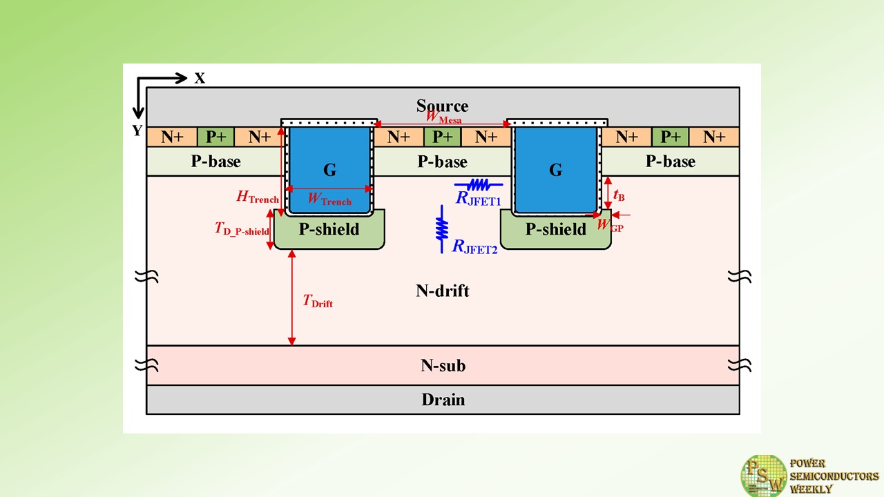
Figure 1 shows the cross-sectional views of the conventional trench MOSFET with grounded P-shield layers (GP-TMOS) and the proposed TMOS with D-pMOS. The proposed TMOS is derived from the GP-TMOS, but it has two unique structural features.
To create a depletion-mode pMOS, a lightly doped P-type layer is positioned between the P+ layer and the P-shield layer. In addition, the poly-Si gate is split into two parts, called the main gate (MG) and the auxiliary gate (AG). The MG controls the n-MOS, while the AG controls the D-pMOS. The two device structures share the device parameters as those listed in Table 1.
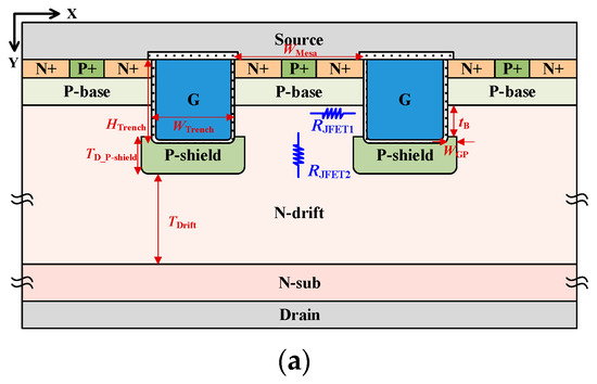
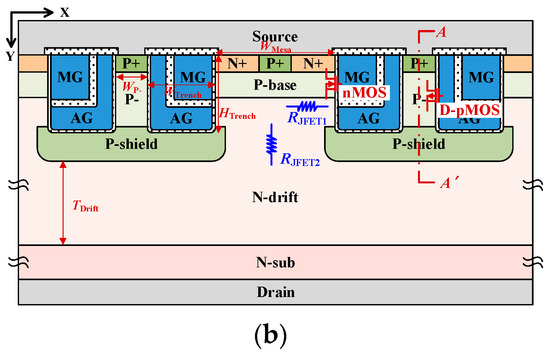
Figure 1. Cross-sectional views of (a) the conventional GP-TMOS, and (b) the proposed TMOS.
Table 1. Device parameters for TCAD simulations.
The RJFET of the GP-TMOS consists of two parts, as shown in Figure 1a. RJFET1 is formed between the P-base and P-shield, and RJFET2 is formed between adjacent P-shield layers. They can be expressed as
Here, WGP is the horizontal distance of the P-shield layer beyond the gate trench. WD_P-shield is the depletion region width of the P-shield/N-drift junction. WD_P-base is the depletion region width of the P-base/N-drift junction. tB is the vertical distance between P-base and P-shield. TP-shield is the thickness of the P-shield layer. VD is the potential of the P-shield/N-drift junction. According to Equation (3), the P-shield layer potential VD determines the extent of the depletion region in the JFET region of TMOS.
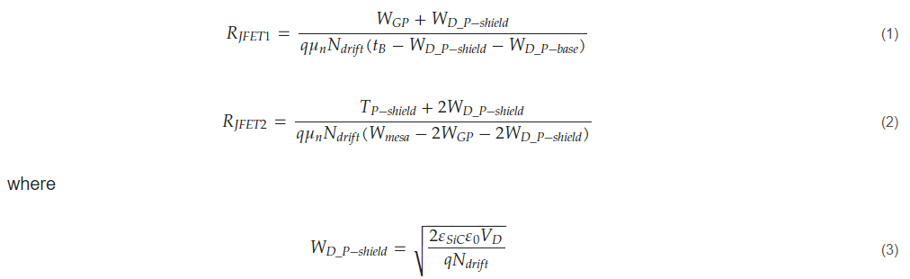
In the forward on-state, the P-shield layer of the proposed TMOS is disconnected from the source electrode by turning off the D-pMOS, and its potential is affected and increased by the voltage of the AG. Figure 2 shows the current density distributions for the GP-TMOS and the proposed TMOS at VMG = 18 V and VAG = 18 V. In the linear operation (Vds = 1 V), the depletion region width (WD) of the P-shield/N-drift junction for the proposed TMOS is smaller than that of the GP-TMOS, as illustrated in Figure 2a,b.
The current path width of the proposed TMOS is widened to decrease RJFET. In the saturation operation (Vds = 800 V), WD for the proposed TMOS is the same as that of the GP-TMOS, as well as the current path width in a single-cell pitch, as shown in Figure 2c,d. This indicates that RJFET1 and RJFET2 of the proposed TMOS are equal to those of the GP-TMOS in a single-cell pitch. Due to a relatively large cell pitch, the saturation current (Jsat) of the proposed TMOS can be remarkably reduced for the same active area. Thus, the proposed TMOS achieves a superior tradeoff relationship between RON, sp and SC capability.
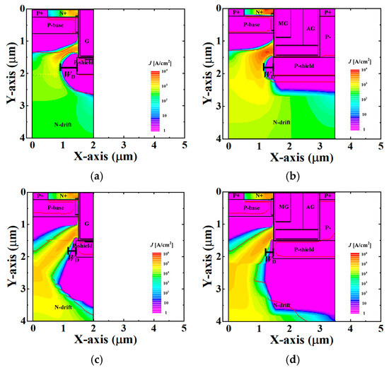
Figure 2. Current density distributions of two devices. (a) GP-TMOS at Vds = 1 V; (b) the proposed TMOS at Vds = 1 V; (c) GP-TMOS at Vds = 800 V and (d) the proposed TMOS at Vds = 800 V.
Figure 3a depicts the energy band diagram of the sandwiched P-type layers along the cutline A-A’ (shown in Figure 1b). When VAG = 0 V, the hole barrier between the P+ layer and the P-shield layer is small. The lightly doped P- layer can transport holes from the P-shield to P+, as shown in Figure 3b, indicating that the P-shield layer is grounded.
When VAG = 18 V, the EV from the P-shield layer to the P- layer decreases, resulting in a hole barrier. This is because the lightly doped P-layer is completely depleted, preventing holes’ transportation from the P-shield layer to the P+ layer, as shown in Figure 3c. This means that the P-shield layer is disconnected from the source electrode and is floating.
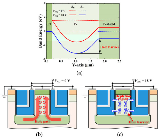
Figure 3. (a) Energy band diagram of the sandwiched P-type layers along the cutline A-A’, and operation mechanisms at (b) VAG = 0 V and (c) VAG =18 V.
In the blocking voltage state, the P-shield layer of the proposed TMOS is connected to the source electrode by turning on the D-pMOS, similar to that of the GP-TMOS. The grounded P-shield layer protects the gate oxide from the high electric field, and then maintains a reliable blocking high voltage capability.
During the switching transient, the P-shield layer of the proposed TMOS is also connected to the source electrode for safe operation. This is because the TMOS with floating P-shield layers has a notorious drawback, which is called dynamic on-resistance degradation. The proposed TMOS has an additional gate electrode, but only one set of gate drivers is required, as shown in Figure 4a.
Using two gate drive resistances, RAG-g and RMG-g, nMOS and D-pMOS can operate asynchronously. Figure 4b shows the waveforms of the MG voltage and AG voltage. The D-pMOS is set to turn off after the nMOS has turned on, keeping the P-shield layer grounded during the switching transient for reliable dynamic operation.
Figure 4. (a) Simplified diagram of the gate driver principle; (b) waveforms of two gate voltages.
3. Simulation Results and Discussion
The physical models include recombination models, incomplete ionization models, mobility models, bandgap narrowing models, and impact ionization models. It is noted that the Giga module is employed to capture self-heating effects and thermoelectric powers. The channel mobility of the TMOS is fixed to 50 cm2/V·s. In this comparison, the numerical simulation parameters are identical.
Figure 5 shows the impact of the width, WP-, and the doping concentration of the lightly doped P- layer, NP-, on the RON, sp (VMG = 18 V, VAG = 18 V and Jds = 200 A/cm2) and Jsat (VMG = 18 V, VAG = 18 V and Vds = 800 V) values of the proposed TMOS. As WP- and NP- decrease, RON, sp decreases and then remains at a fixed value. This is because the electrical connection state of the P-shield layer changes from grounded to floating. A small WP- and a low NP- facilitate the depletion of the P- layer. In contrast, Jsat increases as WP- and NP- decrease. The maximum Jsat is still below 6.5 kV/cm2 due to the relatively large cell pitch for the proposed TMOS.
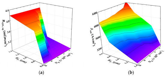
Figure 5. Impact of WP- and NP- on (a) RON, sp and (b) Jsat for the proposed TMOS.
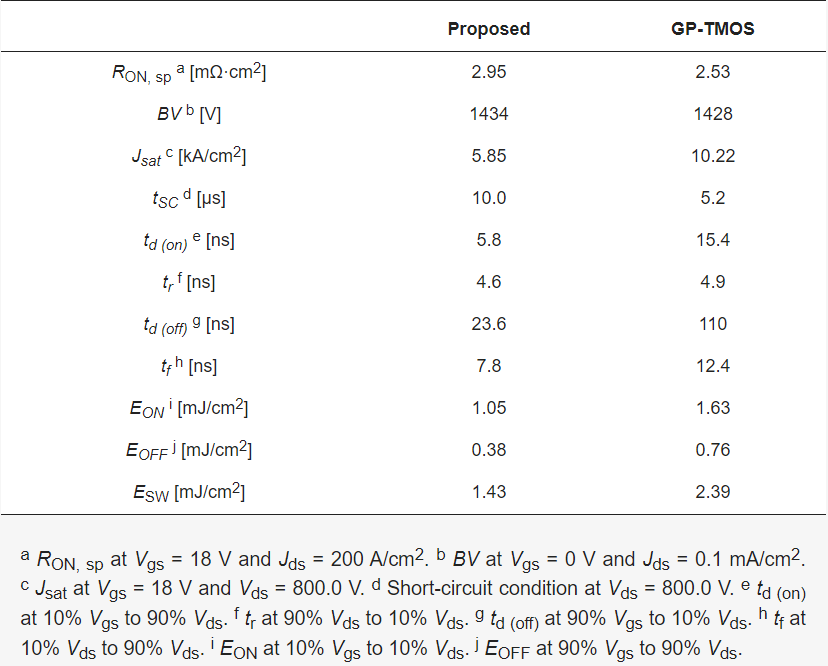
Figure 6 shows the forward output characteristics for the proposed TMOS and the GP-TMOS. The WP- and NP- of the proposed TMOS are 1.0 μm and 4.0 × 1016 cm−3. The RON, sp of the proposed TMOS and the GP-TMOS is 2.95 mΩ·cm2 and 2.53 mΩ·cm2 with Vgs = 18 V and Jds = 200 A/cm2, respectively. The RON, sp of the proposed TMOS is approximately 10% higher than that of the GP-TMOS, whereas the Jsat of the proposed TMOS is substantially reduced from 10.22 kA/cm2 to 5.85 kA/cm2, a reduction of nearly 43%.
Figure 7 shows the blocking voltage characteristics. The P-shield layer of the proposed TMOS is grounded (VMG = 0 V and VAG = 0 V). The blocking behavior of the proposed TMOS is similar to that of the GP-TMOS. The maximum electric field of both is located at the P-shield/N-drift junction.
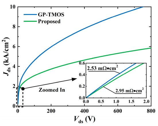
Figure 6. The output characteristics of the proposed TMOS and the GP-TMOS.
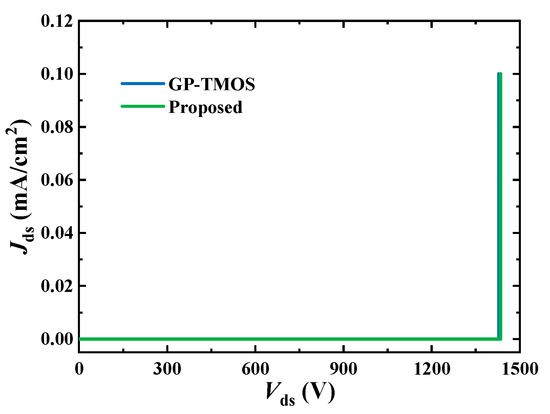
Figure 7. The blocking characteristics of the proposed TMOS and the GP-TMOS.
Figure 8 displays the SC-simulated waveforms of the current density, Jds, and the temperature profile for both the proposed TMOS and the GP-TMOS with Vgs = 18 V and Vds = 800.0 V. The peak current density of the proposed TMOS is decreased by 30%. Therefore, the junction temperature of the proposed TMOS is also lower, which could postpone the triggering of thermal runaway. Compared to the GP-TMOS, the SC withstanding time (tSC) of the proposed TMOS increases from 5.2 μs to 10.0 μs, which is approximately 1.92 times longer. The new design concept significantly eases the tension between RON, sp and tSC.
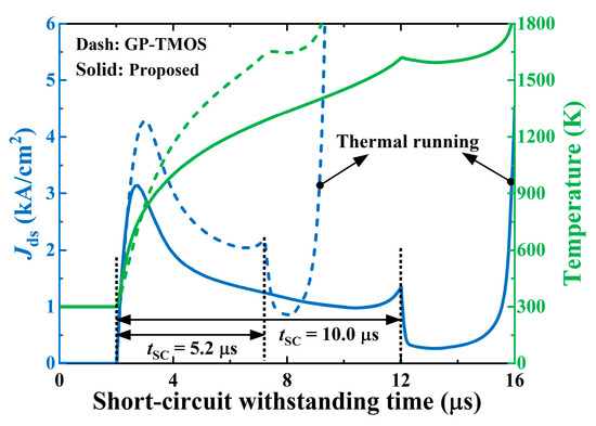
Figure 8. Short-circuit waveforms of the proposed TMOS and the GP-TMOS.
Figure 9 shows the schematic diagram of the dynamic switching simulation. The switching voltage and current are set to 800.0 V and 20.0 A, respectively. The stray inductance in the power loop is 5 nH. Figure 10 shows the influences of the AG resistance, RAG-g, and the doping concentration of the P-layer, NP-, on the power loss of the proposed TMOS. The power loss includes turn on loss and turn off loss. The RMG-g is set to 5, 10, and 20 Ω, and the dependence relationships are shown in Figure 10a–c. As NP- and RAG-g increase, the power loss decreases for various RMG-g.
This is caused by the change in the P-shield layer’s connection state during the switching transient, from a floating state to a grounded state. The TMOS with floating P-shield layers has poor dynamic performance and exhibits relatively higher switching loss. As NP- increases, a relatively high AG voltage is required to fully deplete the P-layer, which affects the threshold voltage of the D-pMOS. On the other hand, increasing RAG-g delays the triggering of the D-pMOS’s turn off during the turn on stage of the proposed TMOS. Both of the above methods can achieve grounded P-shield layers during the switching on transient of the proposed TMOS.
Figure 11 shows the switching waveforms of the proposed TMOS under two conditions. Condition I is NP- = 1 × 1016 cm−3 and RAG-g = 1 Ω, while condition II is NP- = 4 × 1016 cm−3 and RAG-g = 20 Ω. Under condition I, the D-pMOS turns off before the nMOS turns on. The turn on behavior of the proposed TMOS is the same as that of the TMOS with floating P-shield layers, where the expanding depletion region of the P-shield/N-drift junction cannot shrink back immediately, resulting in a slower switching speed and dynamic RON degradation. Under condition II, the D-pMOS turns off after the nMOS turns on. The switching performance is obviously improved by grounding the P-shield.
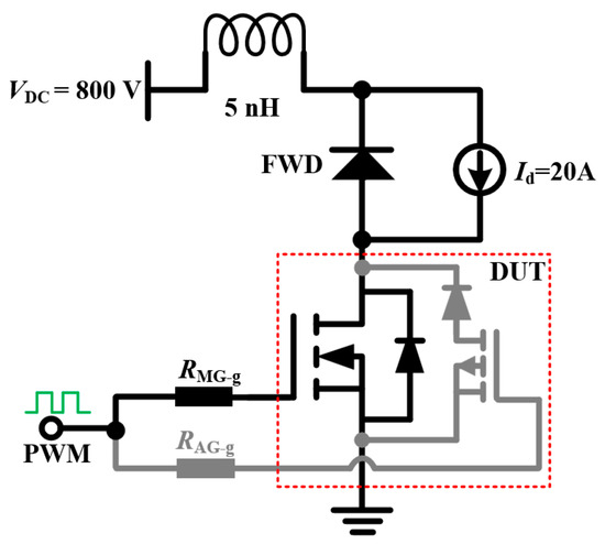
Figure 9. The schematic diagram of the dynamic switching simulation.
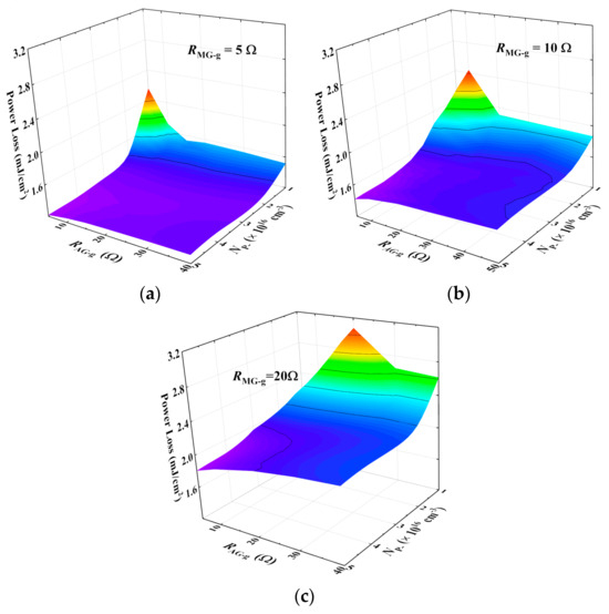
Figure 10. Influences of RAG-g and NP- on the power loss, when (a) RMG-g = 5 Ω, (b) RMG-g = 10 Ω, and (c) RMG-g = 20 Ω.
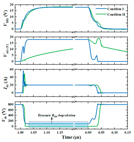
Figure 11. Switching waveforms of the proposed TMOS for condition I (NP- = 1 × 1016 cm−3, RAG-g = 1 Ω) and condition II (NP- = 4 × 1016 cm−3, RAG-g = 20 Ω).
Figure 12 compares the switching waveforms for the proposed TMOS and the GP-TMOS. Both the gate resistance of the GP-TMOS and the MG resistance of the proposed TMOS are set to 10 Ω. The NP- and RAG-g of the proposed TMOS are 4.0 × 1016 cm−3 and 5 Ω, respectively. The optimized AG resistance ensures a reliable switching operation without dynamic RON degradation. Moreover, the switching speed of the proposed TMOS is improved, due to the split-gate structure.
The proposed TMOS exhibits a shorter switching time as a result of its lower gate drain capacitance. The tON and tOFF of the SFP-SG-MOSFET are both smaller than those of the GP-TMOS and decrease by 48.7% and 74%, respectively. The switching power losses are calculated as shown in Figure 13. The turn on loss (EON) for the proposed TMOS is 1.05 mJ/cm2, which is reduced by about 35.5% compared to the GP-TMOS. The turn off loss (EOFF) for the proposed TMOS is 0.38 mJ/cm2, which is reduced by about 50% compared to that of the GP-TMOS.
The total switching loss (ESW) for the proposed TMOS is as low as 1.43 mJ/cm2, showing a 40% reduction compared to that of the GP-TMOS. The performance comparison of the two devices is offered in Table 2.
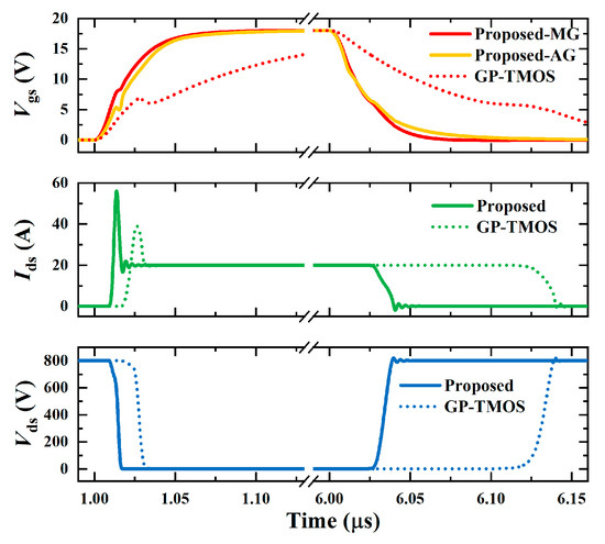
Figure 12. Switching waveforms of the proposed TMOS and the GP-TMOS.
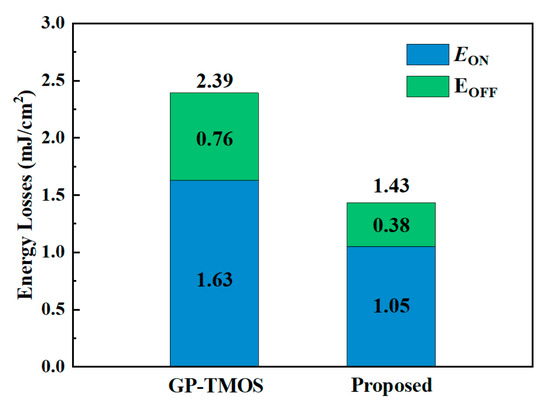
Figure 13. Switching losses of the proposed TMOS and the GP-TMOS.
Table 2. Comparison of two structure device characteristics.
4. Conclusions
A novel 4H-SiC-trench MOSFET with a depletion-mode pMOS (D-pMOS) is proposed and investigated numerically. Using the D-pMOS, the potential of the P-shield layer of the proposed TMOS can be controlled using an auxiliary gate. The width of the depletion region of the P-shield/N-drift junction is adaptively modulated in the linear and saturation operating regions.
Consequently, the proposed TMOS acquires a superior RON, sp—tSC tradeoff, achieving a 92% longer short-circuit withstanding time than that of the GP-TMOS. Moreover, the proposed TMOS flexibly utilizes two different gate resistances, while using only one set of gate drivers, which suppresses the dynamic RON degradation and further reduces switching loss. It achieves a 40% lower switching loss than that of the GP-TMOS. The superior SC capability and lower switching dissipation of the proposed TMOS hold the promise of enhancing the efficiency and reliability of power electronic systems.
Authors
Hengyu Yu, Limeng Shi, Monikuntala Bhattacharya, Michael Jin, Jiashu Qian, Anant K. Agarwal
Original – MDPI