
-

Navitas Semiconductor and SHINRY, global industry leader of on-board power supply and strategic supplier to Honda, Hyundai, BYD, Geely, XPENG, BAIC and many more leading automobile manufacturers, announced the opening of an advanced, joint R&D power laboratory to accelerate the development of New-Energy Vehicle (NEV) power systems enabled by Navitas’ GaNFast™ technology.
Next-gen gallium nitride (GaN) is replacing legacy silicon power chips due to superior high-frequency and high-efficiency characteristics. GaN delivers faster charging, faster acceleration and longer-range, accelerating market adoption of NEVs and the transition from fossil fuels to clean, renewable energy.
On January 16th, 2024, Peter (Jingjun) Chen, COO of SHINRY, along with Navitas’ Gene Sheridan, CEO and Navitas’ Charles (Yingjie) Zha, VP and GM plus other senior executives attended the joint lab’s opening ceremony at SHINRY headquarters in Shenzhen.
The joint lab accelerates development projects, with leading-edge GaN technology combining with innovative system-design skills and engineering talent to enable unprecedented high power density, lightweight, efficient designs that translate to faster charging and extended range, with faster time-to-market.
The joint lab brings together experienced, highly-professional engineers from Navitas and SHINRY to build efficient, collaborative R&D platforms. Navitas’ own dedicated EV system Design Center, located in Shanghai will provide comprehensive technical support for the joint lab.
Navitas will not only supply SHINRY with leading-edge, trusted power devices, but will also engage in system-level R&D from the initial stages of product specification and design, through to test platforms and customized packaging solutions. The result will be more efficient, higher power density, more reliable, and cost-effective power systems for NEVs.
“SHINRY always pursues technological innovation. As early as 2012, SHINRY began applying Silicon Carbide (SiC) MOS, and in 2019, SHINRY initiated research on the application of GaN and has been actively seeking strategic partners.” said Peter (Jingjun) Chen, COO of SHINRY.
“As an advanced supplier in the field, Navitas will assist in creating more advanced, energy-efficient, and higher-efficiency power system products. I believe the establishment of this joint lab will comprehensively accelerate the design and market launch of SHINRY’s products and further enhance the market competitiveness of SHINRY products.”
“We are excited to join with SHINRY to establish a new lab for next-gen power semiconductors, assisting SHINRY in creating advanced power systems.” said Gene Sheridan, Navitas’ co-founder & CEO. “SHINRY’s mission to change the way of travel aligns closely with Navitas’ Electrify Our World™ mission. We believe that through our joint efforts, leading GaN technologies will enter the power systems of NEVs for more end-users, contributing to the vigorous growth of the new energy industry.
Original – Navitas Semiconductor
-

STMicroelectronics N.V. reported U.S. GAAP financial results for the fourth quarter ended December 31, 2023. STMicroelectronics reported fourth quarter net revenues of $4.28 billion, gross margin of 45.5%, operating margin of 23.9%, and net income of $1.08 billion or $1.14 diluted earnings per share.
Jean-Marc Chery, STMicroelectronics President & CEO, commented:
- “FY23 revenues increased 7.2% to $17.29 billion. Operating margin was 26.7% compared to 27.5% in FY22 and net income increased 6.3% to $4.21 billion. We invested $4.11 billion in net CAPEX while delivering free cash flow of $1.77 billion.”
- “In Q4, ST delivered revenues and gross margin slightly below the mid-point of the guidance, with higher revenues in Personal Electronics offset by a softer growth rate in Automotive.”
- “In Q4, our customer order bookings decreased compared to Q3. We continued to see stable end-demand in Automotive, no significant increase in Personal Electronics, and further deterioration in Industrial.”
- “Our first quarter business outlook, at the mid-point, is for net revenues of $3.6 billion, decreasing year-overyear by 15.2% and decreasing sequentially by 15.9%; gross margin is expected to be about 42.3%.”
- “For 2024, we plan to invest about $2.5 billion in net CAPEX.”
- “We will drive the Company based on a plan for FY24 revenues in the range of $15.9 billion to $16.9 billion. Within this plan, we expect a gross margin in the low to mid-40’s.”
Original – STMicroelectronics
-

Acquired by Infineon Technologies in October 2023, GaN Systems has been recognized as the “Graduate Of The Year” by The Global Cleantech 100. The announcement was made at Cleantech Forum North America in San Francisco.
The award recognizes the exceptional contribution legacy GaN Systems has made to sustainable innovation and their successful management team as rated by the financial investors on the 80-member Cleantech Group Expert Panel. This 2024 award rounds out several years of recognition in GaN Systems’ sustainability journey which includes entry in to the Global Cleantech 100 Hall of Fame (1 of only 14 companies ever) and the 2023 Global Cleantech 100 winner (1 of only 100 companies globally in 2023).
The acquisition of GaN Systems has significantly accelerated Infineon’s gallium nitride (GaN) roadmap and further strengthens its leadership in power systems by offering a broad product portfolio combined with leading edge application know-how in the development of GaN-based solutions. Infineon’s expertise and in-depth knowledge in GaN paves the way for more energy-efficient and CO 2-saving technology solutions that support decarbonization.
“My congratulations go out to all legacy GaN Systems employees for this recognition and winning multiple Cleantech awards. We are glad to have these smart and curious minds on board at Infineon,” said Adam White, Division President at Power & Sensor Systems at Infineon. “Thanks to unrivalled R&D resources, a comprehensive understanding of applications and a large number of customer projects, Infineon now leverages the full potential of GaN Systems to become a leading GaN Powerhouse fostering the transformation towards green energy.”
Cleantech® Group is a leading global authority on global cleantech innovation. The Global Cleantech 100 program has been running since 2009. This highly anticipated annual report publishes a list of companies with the most promising ideas in cleantech.
Original – Infineon Technologies
-
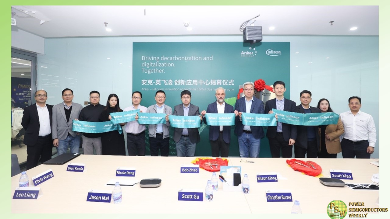
Infineon Technologies AG announced its joint Innovation Application Center in Shenzhen with Anker Innovations, a global leader in charging technology. With the center already fully operating, it is paving the way for more energy-efficient and CO2-saving charging solutions that support decarbonization.
Driven by the growing consumer demand for faster charging solutions due to an increasing usage of mobile devices, laptops and other battery-powered devices, the idea of establishing an Anker-Infineon Innovation Application Center dated back to 2021. After two years of preparation, the joint lab now serves as R&D hub for industry experts to develop power-delivery (PD) fast charging solutions with higher power density, mainly based on Infineon’s next-generation Hybrid Flyback (HFB) controller product family and the CoolGaN™ IPS for fast chargers above 100W.
Anker has already brought several successful products to the market, such as the industry-leading 100W+ fast charger device powered by Infineon’s CoolGaN in 2022. With the Innovation Application Center Anker and Infineon will even shorten the application cycle and accelerate the time to market for future products.
“Anker is an important customer for Infineon,” said Christian Burrer, Vice President of Systems & Application Marketing of Power & Sensor Systems Division at Infineon Technologies. “We have already started a strong cooperation in the charging field, with product and system solutions covering several Infineon product lines. In the field of PD charging, we provide our customers a comprehensive product portfolio, including state-of-the-art power controllers, first-class switching power supplies, leading silicon MOSFET and GaN transistor performance, and more.”
Beyond charging solutions, the joint lab is focusing on a more diversified range of consumer applications, driven by Infineon’s expertise in wide-bandgap materials such as gallium nitride (GaN). The acquisition of GaN Systems in 2023 has significantly accelerated Infineon’s GaN roadmap and further strengthens its leadership in power systems through mastery of all relevant power semiconductor technologies.
“In 2023, Anker achieved success in many markets such as China and Europe. This would not have been possible without Infineon’s GaN technology solutions and the strong collaboration between our companies. We look forward to even intensifying our partnership with Infineon”, said by Kang Xiong, General Manager of the charging business unit at Anker Technologies.
Original – Infineon Technologies
-
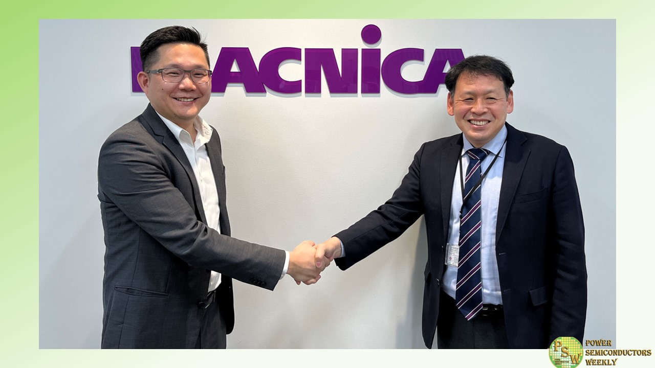
Bourns, Inc. announced it is further expanding its sales presence in Japan by signing Macnica Altima Company as a new distributor partner. Macnica Altima Company was selected for their excellent Japanese Tier 1 customer relationships, especially those in the automotive market, and will be representing Bourns’ full line of standard component products.
“Adding Macnica is part of Bourns’ strategic sales channel growth initiative in Asia. Bourns continues to realize increasing demand for our products from across the Asia-Pacific region. We were looking for a strong, knowledgeable business partner in Japan and found it with Macnica’s excellent sales team,” said James Harrington and Senior Vice President of Worldwide Sales at Bourns.
“We are honored to be selected to represent Bourns’ innovative components in Japan. Macnica is known for our trusted sales and support teams that have particular knowledge of next generation vehicle applications. We offer the full strength of our organization’s market and technical expertise to Bourns in helping them realize continued growth and success in Japan,” said Kazuyuki Sawada, Vice President at Macnica Altima Company.
Original – Bourns
-
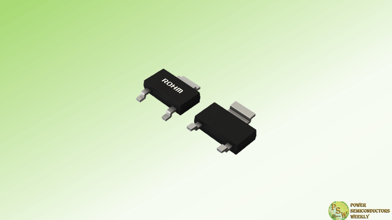
ROHM has added a lineup of compact 600V Super Junction MOSFETs R6004END4 / R6003KND4 / R6006KND4 / R6002JND4 / R6003JND4. These devices are ideal for small lighting power supplies, pumps, and motors.
In recent years, power supplies for lighting and motors for pumps are required to be smaller as devices become more sophisticated – spurring the demand for compact MOSFETs that are essential for switching operation.
Generally, however, it has been difficult to reduce the size of Super Junction MOSFETs while maintaining an optimal balance between high breakdown voltage and low ON resistance. In response, after reviewing the shape of the mounted chip, ROHM was able to develop 5 models in the SOT-223-3 package (6.50mm × 7.00mm × 1.66mm) – providing a smaller, lower profile form factor without compromising the performance of conventional products.
Compared to the conventional TO-252 package (6.60mm × 10.00mm × 2.30mm), ROHM’s new products reduce area and thickness by 31% and 27% – contributing to smaller, lower profile applications. At the same time, the same land pattern (footprint) as the TO-252 package can be used, enabling mounting on existing circuit boards without modification.
Offering distinctive features, three of the models optimized for compact power supplies. The R6004END4, characterized by low noise, is suitable for applications where noise is a concern, while the R6003KND4 and R6006KND4, capable of high-speed switching, are ideal for sets requiring low loss, high efficiency operation.
The R6002JND4 and R6003JND4 utilize proprietary PrestoMOS technology to achieve significantly lower switching losses by speeding up reverse recovery time (trr), making them well-suited for motors-equipped devices.
Supporting materials such as application notes, technical documents, and SPICE simulation models for each product are available on ROHM’s website free of charge to enable quick market introduction.
Going forward, ROHM will continue to expand its Super Junction MOSFET lineup in different packages and even lower ON resistances that contribute to solving social issues such as environmental protection by reducing power consumption in variety devices.
Product Lineup
For compact power supplies
Part No. Data
SheetPolarity
[ch]VDSS
[V]ID
[A]RDS(on) [Ω]
*VGS=10VQg [nC]
*VGS=10VPackage
[mm]Typ. Max. Typ. R6004END4 N 600 2.4 0.90 0.98 15 
SOT-223-3
(6.50×7.00×1.66)R6003KND4 1.3 1.30 1.50 8 R6006KND4 2.8 0.72 0.87 12 For motors
Part No. Data
SheetPolarity
[ch]VDSS
[V]ID
[A]RDS(on) [Ω]
*VGS=15VQg [nC]
*VGS=15Vtrr
[ns]Package
[mm]Typ. Max. Typ. Typ. R6002JND4 N 600 1.0 2.50 3.25 7 40
SOT-223-3
(6.50×7.00×1.66)R6003JND4 1.3 1.65 2.15 8 42 Application Examples
• R6004END4 / R6003KND4 / R6006KND4: Lighting, Air conditioners, Refrigerators, etc.
• R6002JND4 / R6003JND4: Motors for pumps, fans, copiers, etc.Original – ROHM
-
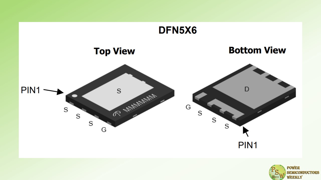
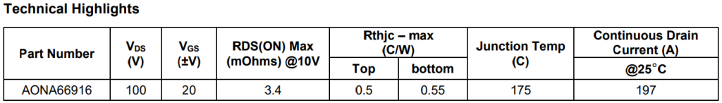
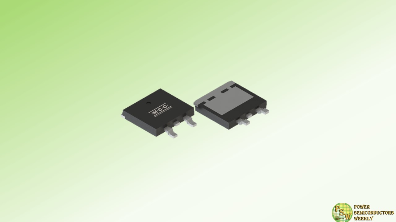
Alpha and Omega Semiconductor Limited (AOS) announced the AONA66916, a 100V MOSFET packaged in the company’s innovatively designed top and bottom side cooling DFN 5 x 6 package. Designers have long trusted AOS power semiconductors as essential components that help them meet a wide variety of high performance application requirements.
Now, in delivering a state-of-the-art package that keeps its semiconductor products cooler, AOS is taking a huge step in enabling engineers to develop more efficient designs in telecommunications and industrial applications that must frequently operate in harsh conditions.
Typically, when using the standard DFN 5×6 package, the bottom contact is the main contributor for cooling, and most of the heat generated by the Power MOSFETs will be transferred to the PCB. This increases the PCB thermal management design considerations to meet system requirements. AOS’ new top and bottom cooling DFN 5×6 package is designed to achieve the highest heat transfer between the exposed top contact and heat sink due to its large surface contact area construction.
This allows the device to achieve a low thermal resistance (Rthc-top max) of 0.5°C / W with results being transferred to the PCB board, enabling significant thermal performance improvements. The top exposed DFN 5×6 package of the AONA66916 shares the same 5mm x 6mm footprint as AOS’ standard DFN 5×6 package, eliminating the need to modify existing PCB layouts.
Another benefit of the AONA66916 is that it utilizes AOS’ 100V AlphaSGT™ technology, providing excellent FOM for balanced performance in hard switching applications. AONA66916 has a maximum RDS(on) rating of 3.4mOhms and has a 175°C junction temperature rating.
“Cooling the power MOSFET in high power design can be challenging, and AOS has successfully addressed this essential issue with our advanced top exposed package design. It not only enables better thermal transfer from its top side exposed contact to heat sink due to large exposed surface area, our new package delivers a much cooler device that contributes to a more efficient and robust final design,” said Peter H. Wilson, Marketing Sr. Director of the MOSFET product line at AOS.
Original – Alpha and Omega Semiconductor
-

Texas Instruments Incorporated reported fourth quarter revenue of $4.08 billion, net income of $1.37 billion and earnings per share of $1.49. Earnings per share included a 3-cent benefit that was not in the company’s original guidance.
Regarding the company’s performance and returns to shareholders, Haviv Ilan, TI’s president and CEO, made the following comments:
- “Revenue decreased 10% sequentially and 13% from the same quarter a year ago. During the quarter we experienced increasing weakness across industrial and a sequential decline in automotive.
- “Our cash flow from operations of $6.4 billion for the trailing 12 months again underscored the strength of our business model, the quality of our product portfolio and the benefit of 300mm production. Free cash flow for the same period was $1.3 billion.
- “Over the past 12 months we invested $3.7 billion in R&D and SG&A, invested $5.1 billion in capital expenditures and returned $4.9 billion to owners.
- “TI’s first quarter outlook is for revenue in the range of $3.45 billion to $3.75 billion and earnings per share between $0.96 and $1.16. We now expect our 2024 effective tax rate to be about 13%.”
Original – Texas Instruments
-

Qorvo® unveiled an automotive-qualified silicon carbide (SiC) field effect transistor (FET) offering an industry-best 9mΩ RDS(on) in a compact D2PAK-7L package. This 750V SiC FET is the first in a new family of pin-compatible SiC FETs from Qorvo with RDS(on) options up to 60mΩ, making them well suited for electric vehicle (EV) applications, including on-board chargers, DC/DC converters and positive temperature coefficient (PTC) heater modules.
The UJ4SC075009B7S features a 9mΩ typical RDS(on) at 25°C needed for reducing conduction losses and maximizing efficiency in high voltage, multi-kilowatt automotive applications. Its small, surface-mount package enables automated assembly flows and reduces customer manufacturing costs. This new 750V family complements Qorvo’s existing 1200V and 1700V automotive SiC FETs in D2PAK packaging to form a complete portfolio addressing EV applications that span 400V and 800V battery architectures.
Ramanan Natarajan, director of Product Line Marketing for Qorvo’s Power Products, said, “The launch of this new family of SiC FETs demonstrates our commitment to providing EV powertrain designers the most advanced and efficient solutions for their unique automotive power challenges.”
These fourth generation SiC FETs leverage Qorvo’s unique cascode circuit configuration, in which a SiC JFET is co-packaged with a Si MOSFET to produce a device with the efficiency advantages of wide bandgap switch technology and the simpler gate drive of silicon MOSFETs. Efficiency in SiC FETs is dependent on conduction losses, and Qorvo’s cascode/JFET approach enables reduced conduction losses through industry-best RDS(on) and body diode reverse voltage drop.
The key features of the UJ4SC075009B7S include:
- Threshold voltage VG(th): 4.5V (typical) allowing 0 to 15V drive
- Low body diode VFSD: 1.1V
- Maximum operating temperature: 175°C
- Excellent reverse recovery: Qrr = 338 nC
- Low gate charge: QG = 75 nC
- Automotive Electronics Council (AEC) Q101-qualified
Original – Qorvo
-
MCC Semi launched the components engineered to satisfy the diverse requirements of demanding applications: eight low-profile Schottky barrier rectifiers with a common cathode configuration, low forward voltage, and countless possibilities.
A sleek and compact TO-263AC package delivers a typical height of only 1.7mm, translating to compatibility with the popular D2PAK footprint and seamless integration into existing designs.
Engineered to reduce power losses and optimize performance you can count on, these components are available in working voltage ranges from 45V to 200V and a forward current of 20A to 30A per device.
Ideal for freewheeling diodes, switch-mode power supplies, motor controls, and many other rugged applications, MCC’s selection of Schottky barrier rectifiers is a go-to solution when space is limited, but expectations are not.
Features & Benefits:
- Low forward voltage design minimizes power losses
- Low-profile TO-263AC package with a typical height of 1.7mm for space-saving performance
- Compatible with the popular D2PAK footprint for added versatility
- Wide working voltage range from 45V to 200V
- Forward current options of 20A and 30A per device
Original – Micro Commercial Components