-

Wise-integration, a French pioneer in digital control of gallium nitride (GaN) and GaN ICs for power supplies, announced financing of €15 million. The Series B round wasled by imec.xpand, with participation from Supernova Invest, BNP Paribas Developpement, Région Sud Investissement (RSI), Creazur, CASRA Capital and Angels for Greentech.
The round will fuel mass production and commercial deployment of the company’s flagship products, WiseGan® and WiseWare®, its disruptive digital-control technology, and its support for clients globally as they adopt these solutions. It included the five investors from the previous funding and three new investors.
CEO Thierry Bouchet said, “The €15 million of new funding will accelerate the company’sinternational expansion, ongoing R&D programs and the introduction of new products and solutions. “This funding will enable Wise-integration to accelerate our commercial development and product development and the launch of a new generation of high-performance GaN technology, which is designed to seamlessly integrate with digital controls and boost the efficiency and performance of power systems across various sectors,” Bouchet continued. “A third roadmap focus will be to broaden our WiseWare® product development, targeting high-value markets, such as industrial, telecom and automotive sectors.”
Since its launch in 2020, the fabless company has established itself as an award-winning innovator in the power electronics industry, building a portfolio of more than 10 patent families. WiseGan® encompasses GaN power integrated circuits designed to maximize the benefits of GaN technology, including higher power density, efficiency and reduced heat generation. WiseWare® is a 32-bit, MCUbased, AC-DC digital controller optimized for GaN-based power supply architectures, offering simplified system design, a lower bill of materials and improved power density and efficiency.
The company’s target markets include consumer electronics, from laptops to e-bikes, scooters and motorcycles, to industrial applications like robotics, as well as data centers and electric vehicles. All its solutions address the increasing demands for miniaturization, electrification and efficient power management.
Wise-integration has established a first-class semiconductor GaN supply chain to support its mass production and commercialization strategy, while ensuring the most competitive costs in the market.
“Wise-integration’s GaN technology can play a significant role in the global shift to electrification by enhancing the efficiency and performance of power systems across various sectors,” said Cyril Vančura, imec.xpand partner. “In the four years since its founding, this start-up has demonstrated the vision, drive, execution and technological knowhow to deliver game-changing power-electronics solutions, and we look forward to witnessing the next phase of its growth journey.”
“With this new funding, Supernova Invest reaffirms its support for Wise-integration, a CEA-Leti spinoff that we have trusted since its creation,” said Damien Bretegnier, investment director, Supernova Invest. “We strongly believe in the huge potential of its WiseWare® digital control technology and associated WiseGan® components, anticipating a profound revolution in the power conversion market that propels GaN technology to replace legacy solutions even more rapidly.”
“Wise-integration is one of the finest up and-coming companies in the hardware sector, a key sector in our beautiful region,” said Pierre Joubert, general director of RSI. “A high-potential company with a top management team, it fits in perfectly with the investment thesis of our Transition fund and its 100 percent Paris Agreement strategy. It has all the assets to become one of the strong links in the regional economic development strategy.”
Original – Wise-integration
-

Okmetic is celebrating the 25th anniversary of its North American sales office. Okmetic Inc. was established in Allen, Texas in 1999 to strengthen Okmetic sales and technical support to the North American customer base. The Okmetic, Inc. office continues to be based in Allen, Texas with local commercial support across North America.
Initially, the business was focused on selected silicon products but has since expanded to support not only traditional semiconductor materials but also engineered products used for the Communication, RF filter, MEMS, Power, and AI just to highlight a few. The NA customer region, along with the European and Asian regions, work together using a balanced approach to serve the Okmetic worldwide market.
The team at Okmetic Inc. continues to be recognized for support efforts in the industry. Some of these include supplier award recognition, numerous conference speaking and exhibiting engagements, as well as a lifetime achievement recognition for company’s participation with organizations such as SEMI.
“We want to thank our customers for entrusting us to be a key component of their business growth strategy, inspiring us to continuously raise the bar and cooperatively develop silicon products that enable our lives each day. As we continue to expand our capacity to build for our future, we are excited to partner more closely with our customers to develop the needed products and support to enable their ongoing business needs “, says Jim Reed, President of Okmetic Inc.
Original – Okmetic
-

Ideal Power Inc. reported the results for its fourth quarter and full year ended December 31, 2023.
“We made great progress delivering against our B-TRAN™ commercial roadmap in 2023 and that progress has continued into 2024,” said Dan Brdar, President and Chief Executive Officer of Ideal Power. “Strong momentum continues with participants in our test and evaluation program, particularly for solid-state circuit breaker and hybrid and electric vehicle applications. We expect to convert large OEMs into design wins and/or additional custom development agreements this year.”
Brdar continued, “We recently completed Phase II of our development agreement with Stellantis and commenced shipment of SymCool™ power modules to fulfill customer orders. We expect industrial markets, particularly the solid-state circuit breaker market served by our SymCool™ power module, to be the earliest source of our product sales ramp.”
Key Fourth Quarter and Recent Operational Highlights
- Commenced commercial shipment of SymCool™ power modules to fulfill customer orders. The SymCool™ power module targets several applications including solid-state switchgear and circuit protection, renewable energy inverters for solar and wind, industrial inverters, hybrid and electric vehicles (“EVs”) and EV charging.
- Successfully completed Phase II of a product development program with Stellantis, a top 10 global automaker. All Phase II deliverables were completed ahead of schedule including a wafer run and deliveries of tested B-TRAN™ devices, drivers and a Stellantis approved comprehensive reliability test plan for automotive qualification. Ideal Power is partnering with Stellantis’ advanced technology development team to develop a custom B-TRAN™ power module for use in EV drivetrain inverters in Stellantis’ next generation EV platform.
- Stellantis recognized Ideal Power and its program with Stellantis as a finalist in the 2023 Stellantis Venture Awards, which was the result of the excellent performance of the commercial B-TRAN™ devices provided to the Stellantis team for testing and evaluation.
- Released B-TRAN™ and SymCool™ videos and application notes for the technical audience at prospective customers, resulting in the addition of new opportunities to our sales funnel. The videos demonstrate the testing of discrete B-TRAN™ devices and SymCool™ power modules and the compelling advantages B-TRAN™ offers to solid-state circuit breaker applications.
- Nearing completion of a qualification run with our second high-volume wafer fabrication partner. This wafer fab in Europe will support future revenue growth and add dual sourcing for wafer fabrication.
- B-TRAN™ Patent Estate: Currently at 82 issued B-TRAN™ patents with 36 of those issued outside of the United States and 39 pending B-TRAN™ patents. Current geographic coverage includes North America, China, Japan, South Korea, India, and Europe, with pending coverage in Taiwan.
Fourth Quarter and Full Year 2023 Financial Results
- Commercial revenue increased to $61,483 in the fourth quarter of 2023 from $0 in the fourth quarter of 2022. Commercial revenue increased to $161,483 for the full year 2023 from $0 for the full year 2022.
- Grant revenue was $0 in the fourth quarter of 2023 and $37,388 for the full year 2023 compared to $16,608 in the fourth quarter of 2022 and $203,269 for the full year 2022.
- Operating expenses in the fourth quarter of 2023 were $2.5 million compared to $2.0 million in the fourth quarter of 2022 driven primarily by higher research and development spending.
- Operating expenses in the full year 2023 were $10.4 million compared to $7.3 million in the full year 2022 driven primarily by higher research and development spending and stock-based compensation expense.
- Net loss in the fourth quarter of 2023 was $2.4 million compared to $1.9 million in the fourth quarter of 2022. Net loss in the full year 2023 was $10.0 million compared to $7.2 million in the full year 2022.
- Cash used in operating, investing and financing activities in the fourth quarter of 2023 was $2.3 million compared to $2.1 million in the fourth quarter of 2022. Cash used in operating, investing and financing activities in the full year 2023 was $7.9 million compared to $6.8 million in the full year 2022.
- Cash and cash equivalents totaled $8.5 million at December 31, 2023.
- No long-term debt was outstanding at December 31, 2023.
2024 Milestones
For 2024, the Company has set or achieved the following milestones:
- Successfully completed Phase II of development program with Stellantis
- Secure Phase III of development program with Stellantis
- Complete qualification of second high-volume production fab
- Convert large OEMs in our test and evaluation program to design wins/custom development agreements
- Add distributors for SymCool™ products
- Initial sales of SymCool™ IQ intelligent power module
- Begin third-party automotive qualification testing
Original – Ideal Power
-
Abstract
A SiC double-trench MOSFET embedded with a lower-barrier diode and an L-shaped gate-source in the gate trench, showing improved reverse conduction and an improved switching performance, was proposed and studied with 2-D simulations. Compared with a double-trench MOSFET (DT-MOS) and a DT-MOS with a channel-MOS diode (DTC-MOS), the proposed MOS showed a lower voltage drop (VF) at IS = 100 A/cm2, which can prevent bipolar degradation at the same blocking voltage (BV) and decrease the maximum oxide electric field (Emox).
Additionally, the gate–drain capacitance (Cgd) and gate–drain charge (Qgd) of the proposed MOSFET decreased significantly because the source extended to the bottom of the gate, and the overlap between the gate electrode and drain electrode decreased. Although the proposed MOS had a greater Ron,sp than the DT-MOS and DTC-MOS, it had a lower switching loss and greater advantages for high-frequency applications.
1. Introduction
Nowadays, silicon carbide (SiC) is widely used in many applications because of its high critical electric field and superior thermal conductivity. The SiC MOSFET has a lower on-resistance and a faster switch speed compared with the Si-insulated Gate Bipolar Translator (IGBT). However, the body diode of the SiC MOSFET has a high on-state voltage drop of about 2–3 V because of its wide bandgap.
Additionally, when the body diode operates in bipolar mode, basal plane dislocations (BPDs) and stacking faults (SFs) are generated because of the recombination energy of the electrons and holes, and these faults cover most of the junction area and cause conduction losses to increase. Thus, the SiC MOSFET usually reverse-parallels a freewheeling diode to suppress the body diode; this extra diode not only increases the package size but also increases the parasitic inductance, which limits the switching frequency of the MOSFET.
One possible way of solving this problem is to integrate a unipolar diode into the MOSFET cell—in particular, a Schottky Barrier Diode (SBD)/Junction Barrier Controlled Schottky Diode (JBS). A disadvantage of these integrated unipolar diodes is the increased leakage current in the blocking state for the MOSFET. The use of a built-in channel diode is another option that can improve the reverse-recovery characteristics of the MOSFET, showing better switching characteristics, but the reliability problem caused by thin gate oxide still needs further research.
In recent research, low-barrier diodes (LBDs) have been adopted for their enhanced third-quadrant and switching performance in planar MOSFETs, but the planar structure limits the MOSFET’s usage in high-power applications because of its wide cell pitch and its high specificity of resistance (Ron,sp).
This paper proposes a 1200 V L-shaped split-gate trench SiC MOSFET integrated with a low-barrier diode. This structure can inhibit the reverse conduction of the body diode to avoid the effects of bipolar degradation and to extend the source to the bottom of the gate, forming a split gate to reduce the Crss and to achieve a fast switching speed.
This study was carried out with numerical TCAD, and some essential models were included such as the Fermi–Dirac, incomplete-ionization, Shockley–Reed–Hall and Auger combination, Lombardi (CVT), impact-ionization, and band-narrowing models. A channel mobility of 50 cm2/(Vs) was used. The structure achieved a lower VF, Cgd, and Qgd and lower switching losses compared with a DT-MOS and a DT-MOS with an MOS-channel diode (DTC-MOS), and it also reduced the maximum oxide electric field (Emox).
2. Device Structure and Mechanism
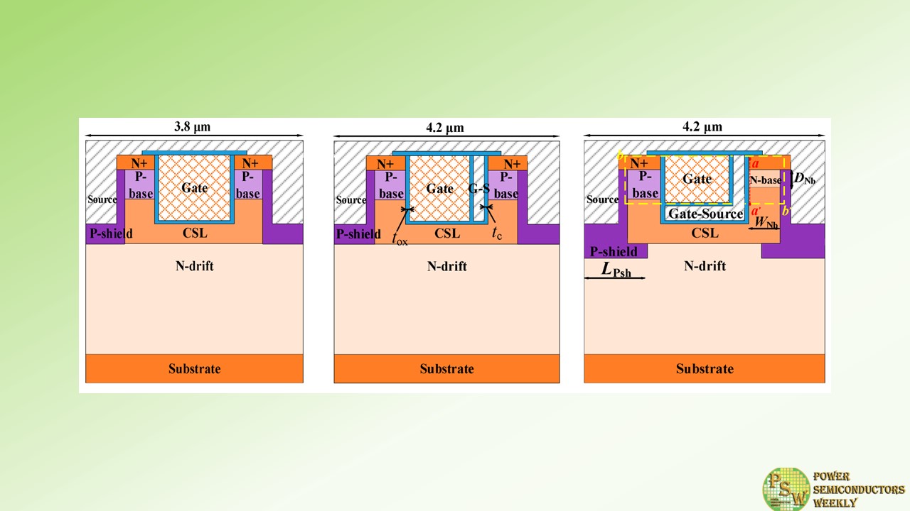
Figure 1 shows the schematic structures of the (a) DT-MOS, (b) DTC-MOS, and (c) proposed MOS. Based on the DTC-MOS, the proposed MOS turns part of the polysilicon gate to the source and extends to the bottom of the gate, forming an “L-shape” split gate. The gate-source connects to the source, so the overlap between the gate and drain decreases, which leads to a decrease in the Cgd. Meanwhile, at the right half-cell, the p-base turns into an n-base, so a low-barrier diode is integrated into this structure to improve its reverse conduction. The P-shield extends to the current spreading layer (CSL), and it decreases the Emox in the blocking state and increases the BV, improving the device’s reliability.
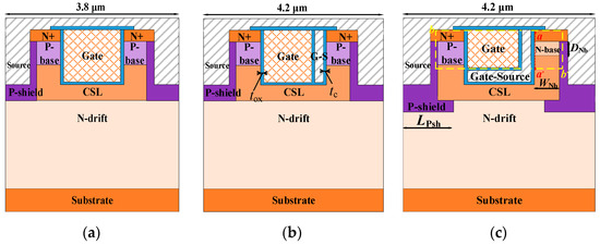
Figure 1. Schematic cross-sectional structures of the (a) DT-MOS, (b) DTC-MOS, and (c) proposed MOSFET.
This device is based on a 4H-SiC, with the doping concentration and thickness of the N-drift set at 8 × 1015 cm−3 and 9 μm, respectively. The P-base region in all the devices had a doping concentration of 2 × 1017 cm−3 and a thickness of 0.5 μm. The N-base had a doping concentration of 3 × 1016 cm−3 and a thickness of 0.3 μm. The P-shield had a doping concentration of 2 × 1018 cm−3 and a thickness of 0.3 μm. The CSL had a doping concentration of 8 × 1016 cm−3 and a depth of 1.7 μm. The depth of the source trench and gate trench was 1.4 μm for both devices. The thickness of the gate oxide was 50 nm for both the N-base and P-base to improve the device reliability in the DT-MOS and proposed MOS. Considering the sufficient volume of the gate and the electric field, the distance of the oxide between the gate and gate-source and the thickness of the gate-source was 0.1 μm for the DTC-MOS and the proposed MOS. The cell pitch was 3.8 μm for the DT-MOS, and that of the other two devices was 4.2 μm. The main structure parameters of the DT-MOS, DTC-MOS, and proposed MOS are shown in Table 1.
Table 1. Structural parameters of the three devices.
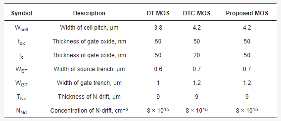
Figure 2a shows the three-dimensional conduction band energy (EC) distribution of the 4H-SiC in the proposed MOS structure at zero bias. The EC decreased from the P-shield to the N-base at the right half-cell. The high doping of the P-shield and the low doping of the N-base led to a rapid depletion of the N-base region at zero bias, preventing the formation of a conducting channel. Therefore, there was no impact on the BV at low doping concentrations.
At zero bias, the EC of the N-base was lower than the P-base, allowing electrons to overcome the potential barrier at a low Vds. Figure 2b shows the EC distribution along the a–a’ line (shown in Figure 1) at different Vds. As Vds decreased, the EC increased in both the N-base and CSL. However, the EC of the CSL increased faster than the N-base region. At Vds = −1 V, the potential barrier became very low, allowing electrons to overcome the potential barrier, turning on the low barrier diode.
Figure 2. (a) Three-dimensional EC distribution of the proposed MOSFET at zero bias (b–b’—the yellow dashed line in Figure 1). (b) EC distribution of the SiO2/SiC interface (a–a’—the red dashed line in Figure 1) at different Vds.
The potential barrier model for LBD in a planar MOSFET is given by:

where ϕSi_SiCand χSi_SiCare the work function and electron affinity difference between the Si and SiC. ɛOX and ɛSiC are the permittivity of the SiO2 and SiC. NNb is the doping concentration of the N-base. The WNb is the width of the N-base. The structure of the low barrier diode in a planar structure and trench structure is the same, being formed by the N+ polysilicon, oxide, the low doping concentration N region, and the high doping concentration P region. Although the formula was obtained for planar structures, it is also applicable to trench structures.
The tc is the thickness of the oxide between the gate-source and the N-base, which is fixed at 50 nm in the proposed MOS, as it has a great influence on device reliability. The tc of the DTC-MOS was 20 nm, to easily turn on the built-in diode. From equation (1), NNb and WNb had an impact on the potential barrier of the LBD. Additionally, the thickness of the N-base (TNb) and the length of the P-shield (LPsh) also influenced the resistance of the LBD, which in turn affects the VF. Therefore, these parameters were optimized.
3. Simulation Results and Analysis
Figure 3a illustrates the impact of WNb and DNb on the BV and VF. The solid circles represent BV values and the dashed circles represent VF values. The WNb varied from 0.1 μm to 0.6 μm in steps of 0.1 μm. As WNb increased, the reverse current path expanded, which led to a decrease in VF. However, the breakdown turned into a punch-through breakdown, which made the device unable to withstand high voltages.
With increasing DNb, the length of the potential barrier increased, leading to an increase in VF. In this case, a longer WNb was required to trigger a punch-through breakdown. It is worth noting that when DNb exceeded 0.3 μm, the leakage current of the proposed MOS became comparable to the DT-MOS, which will be further discussed later. To tradeoff the BV, VF, and leakage current, the optimal values of WNb = 0.3 μm and DNb = 0.3 μm were selected.
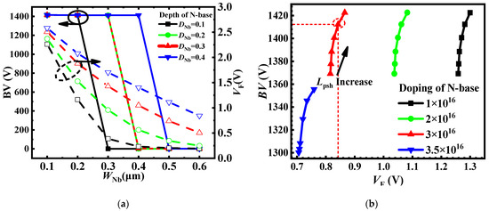
Figure 3. (a) Influence of DNb and WNb on BV and VF; (b) BV, VF at different LPsh and NNb.
Figure 3b shows the tradeoff between the BV and VF for the proposed MOS, considering different values of LPsh and NNb. As the LPsh increased from 1 μm to 1.5 μm in steps of 0.1 μm, the depletion region extended, leading to a decrease in Emox and an increase in BV. However, the current path became narrow, leading to an increase in Ron,sp and VF because of the change in the JFET resistance. With increasing NNb, the potential barrier of the low barrier diode reduced, leading to a decrease in VF.
However, with high doping of NNb, the BV dropped below 1400 V, as shown for NNb = 3.5 × 1016 cm−3. At low NN values, the breakdown point occurred at the P-shield/N-drift junction, so the BV did not change with different NNb values. The change in NNb had no influence on Ron,sp. However, with increasing LPsh, the Ron,sp increased from 1.84 mΩ × cm−2 to 4.58 mΩ × cm−2. In order to tradeoff BV, VF, and Ron,sp, LPsh = 1.3 μm and NNb = 3 × 1016 cm−3 were selected, represented by the red circle in Figure 3b.
The main parameters of the gate trench are shown in Figure 4a. The thickness of the gate trench was fixed at 1.4 μm. Figure 4b shows the influence of the distance between the gate and the gate-source (Dox) on the Cgd and oxide electric field (Eox). The voltage between the gate and the gate-source was set to 15 V. When Dox was 0.1 μm for both the bottom and side wall of the gate, the Eox was 1.5 MV/cm, which corresponds to the simulation results.
The thickness of the gate-source (TGS) was fixed at 0.1 μm, and the thickness of gate poly (TG) changed as Dox increased or decreased. With increasing Dox, the BV and VF had no influence, so they are not included in Figure 4b. The Dox has little influence on Cgd. Therefore, when Dox was greater than 0.1 μm, Eox was already less than 3 MV/cm. In order to facilitate subsequent simulations and ensure a sufficient volume of gate poly for adjusting the gate resistance, Dox = 0.1 μm was selected.
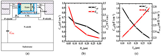
Figure 4. (a) Parasitic capacitance for the Cgd of the proposed MOS. (b) Influence of device characteristics on the distance between the gate and gate-source (c) Influence of Cgd and Ron,sp on the thickness of the gate-source.
The influence of the device characteristics on TGS is shown in Figure 4c; the Dox was fixed at 0.1 μm. With increasing TGS, there was no influence on BV and VF, which is not shown in the figure. Ron,sp increased from 2.23 mΩ∙cm2 to 2.28 mΩ∙cm2, because the CSL, oxide, and gate poly formed an MIS structure, which increased the electron concentration of the CSL during conduction; this effect weakened as TG decreased.
With increasing TGS, Cgd decreases; this is because the gate-source extends to the bottom of the gate poly, resulting in a significant decrease in the overlap between the gate electrode and drain electrode. In this case, the Cgd can be expressed as:

As shown in Figure 4a, Cp is the oxide capacitance between the P-base and gate electrode, which is related to the thickness of the oxide and the overlap between the gate poly and the P-base. CPN is the junction capacitance, which is completely independent of the gate parameters, and the CPN decreases as Vds increases. When increasing TGS or Dox, the TG decreases, resulting in a decreased overlap between the gate poly and the P-base, thus causing a decrease in Cp.
Meanwhile, the TG has no influence on CPN, so the Cgd will decrease. However, it is worth noting that the Cgd is already sufficiently small, and further decreasing Cp cannot significantly change the Cgd. To ensure a suitable gate resistance for device, a sufficient volume of gate poly must be considered, which cannot be reflected in a simulation. Therefore, TGS = 0.1 μm was selected for further simulations.
According to Figure 4b,c, the internal parameters of the gate trench have little influence on the performance of the device when the resistance of the gate poly is not considered; this shows that the proposed MOS has a wide process window for forming the L-shape gate-source.
Figure 5a shows the leakage current and blocking voltage for the three devices. The DT-MOS and proposed MOS blocking voltage exceeded 1400 V. However, the BV of the DTC-MOS was only 1340 V. This indicates that a wide cell pitch results in a decrease in the BV, while the extended P+ shield helps to improve the BV. For the proposed MOS, the leakage current increased faster at DNb = 0.2 μm.
However, when DNb = 0.3 μm, the BV was the same as DNb = 0.2 μm, the leakage current decreased to the level of the DT-MOS. This is because the leakage current is related to the parameters of the N-base before breakdown and the blocking voltage is related to the P-shield/N-drift junction, where the electric field is highest in the SiC region and avalanche breakdown occurs.
The electric field distribution of the three devices at 1200 V is shown in Figure 5b. The Emox was located at the bottom of the oxide for all the devices. Compared with the DT-MOS and DTC-MOS, the proposed MOS had an extended P-shield, which was able to expand the depletion layer and provide better protection effects to the oxide. As a result, the Emox was only 2.52 MV/cm, while the Emox of the other devices was higher than 4 MV/cm.
With a high Emox, a Fowler–Nordheim tunneling current may be generated; this carries electrons through the oxide layer, breaking the Si-O bond over time and generating defects, leading to a full breakdown of the SiO2 layer, which has a great influence on device reliability.
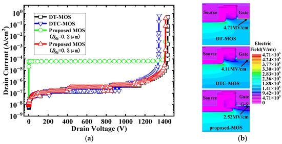
Figure 5. (a) BV characteristics (b) electric field distributions with a drain bias at 1200 V of the DT-MOSF, DTC-MOS, and proposed MOS.
The I–V characteristic is shown in Figure 6a. In forward conduction, the Ron,sp of the DT-MOS and DTC-MOS was smaller than for the proposed MOS; this is because the DT-MOS has two channel paths for conduction, and because both DT-MOS and DTC-MOS do not extend the P-shield, which increases JFET resistance. With a low barrier diode, the VF of the proposed MOS decreased significantly. The VF was 2.85 V, 2.63 V, and 0.85 V at 100 A/cm2 for the DT-MOS, DTC-MOS, and proposed MOS, respectively.
The current vector of the forward and reverse conduction is also shown in Figure 6a. It can be seen that there was only one current path for both conduction conditions. The current flows from the N+ region through the N-base to the drift region in reverse conduction, while the current flows from the drift region through the P-base to the N+ region in forward conduction. Figure 6b shows the hole concentration at Is = 100 A/cm2 of all the devices. In reverse conduction, the drift region of the DT-MOS obtained a high concentration of holes, which causes bipolar degradation.
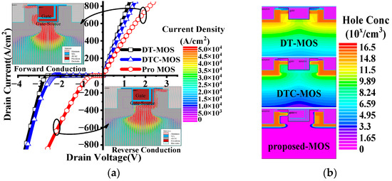
Figure 6. (a) I–V characteristics of the three devices; (b) hole concentration distributions at Is = 100 A/cm2.
The short-circuit (SC) test results for the DT-MOS, DTC-MOS, and proposed MOS are shown in Figure 7. The SC test circuit used in the simulation is shown in Figure 7b. The bus voltage was 800 V. The stray inductance and resistance was 1 nH and 1 mΩ, respectively. The gate resistance was 10 Ω. A single pulse of 0 V/15 V gate bias was applied to the gate contact until the device failed due to thermal runaway caused by excessive temperatures.
The time from device turn-on to failure was 1.6 μs, 1.9 μs, and 2.8 μs for the DT-MOS, DTC-MOS, and proposed MOS, respectively. For the DT-MOS, the highest saturation current caused a faster temperature rise, leading to earlier device failure. Due to the single current channel and depletion layer extension of the P-shield region, the proposed MOS exhibited the lowest saturation current. As a result, the proposed MOS achieved the longest time until failure.
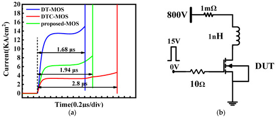
Figure 7. (a) Short circuit characteristics of the three devices; (b) short-circuit test circuit.
In the proposed MOS, the gate-source extended to the bottom of the gate, leading to a decrease in the overlap between the gate and the drain. As a result, the proposed MOS had the lowest Cgd compared to the DT-MOS and DTC-MOS, as shown in Figure 8a. While switching transients, the time constant is determined by the junction capacitance and gate resistors, which impact the switching speed of the devices. With a smaller capacitance, the devices switch at a faster speed.
The Cgd was 141.68 pF/cm2, 136 pF/cm2, and 1.81 pF/cm2 for the DT-MOS, DTC-MOS, and proposed MOS, respectively. Figure 8b shows the gate charge for the three devices; the Qgd of the DT-MOS was 569 nC/cm2 and the Qg (Vgs = 15 V) was 1467 nC/cm2. The Qgd of the DTC-MOS was 406 nC/cm2 and the Qg was 1136 nC/cm2. However, the Qgd of the LST-MOSFET was 6.7 nC/cm2 and the Qg was 333 nC/cm2; this result is consistent with the results for the Cgd, indicating that the proposed MOS can significantly reduce switching losses.
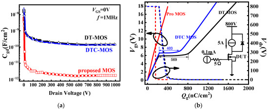
Figure 8. (a) C–V characteristics; (b) Gate Charge of three devices.
The switching waveforms and test circuit of the three devices are shown in Figure 9. Figure 9d shows the resistance switch circuit used in the simulation, with a load current of 10 A (100 A/cm2) at a normal current density. As can be seen in Figure 9a, the proposed MOS exhibited a lower Qgd compared to the other devices. The miller plateau almost disappeared, leading to a faster transition of Vgs, which is consistent with the Cgd results. This characteristic resulted in a significantly faster switching speed for the proposed MOS compared to the other devices, thereby reducing switching losses.
From Figure 9b, the turn-on loss (Eon) and turn-off loss (Eoff) of the DT-MOS was 0.28 mJ/cm2 and 0.47 mJ/cm2 and for the DTC-MOS was 0.26 mJ/cm2 and 0.48 mJ/cm2. However, for the proposed MOS, the Eon and Eoff decreased to 0.09 mJ/cm2 and 0.29 mJ/cm2. The switching losses (ESW) consisted of the Eon and Eoff; the ESW of the proposed MOS was 49.3% and 48.6% lower than that of the DT-MOS and DTC-MOS, respectively.
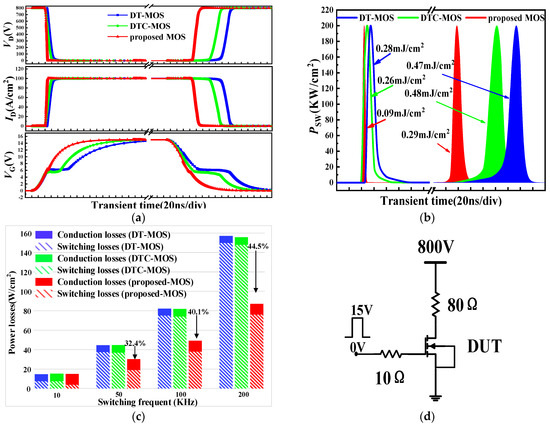
Figure 9. The switching waveforms of the DT-MOS, DTC-MOS, and Proposed MOS, respectively; (a) Turn-on and turn-off waveforms; (b) Turn-on loss and turn-off loss waveforms; (c) total power losses as a function of switching frequency f; (d) resistance switching circuit for simulations.
The total power losses (Pt) consist of conduction power losses and switching losses. When the device is operating under a square wave with a period T and a duty cycle D, the Pt can be expressed as (3):

When the device operated at 100 A/cm2, the Vds was 0.132 V, 0.156 V, and 0.223 V for the DT-MOS, DTC-MOS, and proposed MOS, which is consistent with the Ron,sp. The switching frequency, f, is related to the period, T, by the formula

Although the Ron,sp of the proposed MOS was greater than that of the DT-MOS and DTC-MOS, the switching losses were the main contributor to power loss at high frequencies. Working at high frequencies can effectively reduce the total power losses of the device; it is worth it to increase the on-resistance slightly to achieve smaller switching losses at high frequencies.
Figure 9c shows the total power loss as a function of f for the three devices, when a D of 50% was assumed. When the switching frequency was 50 KHz, the proposed MOS achieved the lowest power loss compared to the other devices due to its lower switching loss. At a switching frequency of 200 KHz, the Pt of the proposed MOS was 44.5% lower than the DT-MOS. With increasing f, the deference in Pt between the DT-MOS and the proposed MOS gradually increased.
The switching condition at a high current density (500 A/cm2) is shown in Figure 10. As the current density increased, both conduction losses and switching losses increased significantly. The ESW of the three devices is shown in Figure 10a. The proposed MOS value was 0.96 mJ/cm2, which was 42.9% and 36.4% lower than the DT-MOS and DTC-MOS.
However, the conduction losses of the proposed MOS increased faster than the other devices at 500 A/cm2. As a result, the Pt of the proposed MOS was the highest before f = 200 KHz, as shown in Figure 10b. At a f of 250 KHz, the Pt of the proposed MOS was only 7.6% lower than that of the DT-MOS. Comparing the work conditions between a normal current density and a high current density, it is more favorable for the proposed MOS to work at a normal current density.
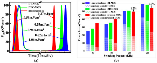
Figure 10. Device works at 500 A/cm2; (a) Turn-on loss and turn-off loss waveforms; (b) total power losses as a function of switching frequency f.
However, high switching speeds and frequencies may present a greater switching oscillation challenge. By adding RC snubbers, reducing the switching speed, or using active gate control techniques, the switching oscillation will be suppressed. However, the mentioned methods for suppressing switching oscillation will lead to an undesirable increase in switching time and switching losses.
There is a tradeoff between power losses and switching oscillation. An electronic structure that has transient part-time symmetry triggered by the switching-on and off of electronic devices can release oscillation energy, while still maintaining the very low loss state. This may be a good choice for suppressing switching oscillation in the future. The comprehensive performance of the three devices is shown in Table 2.
Table 2. Comparison of the three devices’ characteristics.
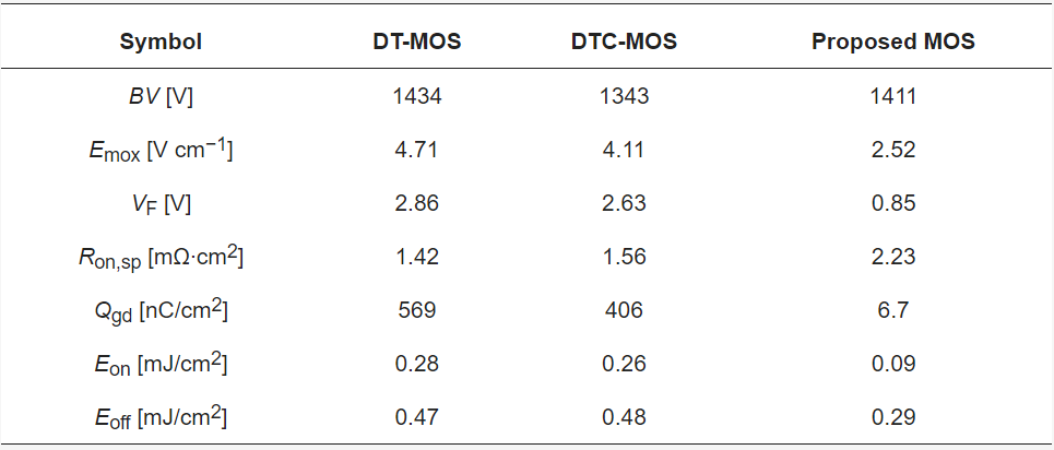
Figure 11 shows a possible process for the proposed MOS. The process starts with the formation of the P-shield region after epitaxy, as shown in Figure 11a. Then, the P-base and N-source are formed by ion implantation followed by high-temperature annealing, as shown in Figure 11b. After this, the gate trench is etched, the gate oxide is formed by chemical vapor deposition (CVD), and the polysilicon is deposited and etched to form the gate-source, which is shown in Figure 11c.
Then, the oxide is deposited and the N+ polysilicon is deposited and etched to form the gate electrode, which is shown in Figure 11d. Figure 11e shows the etching of the source trench and tilted implantation to form the P+ region along the sidewall of the source trench. Finally, Figure 11f shows the deposition of a passivation layer, the etching of the contact window, and the formation of the ohmic contact.
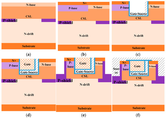
Figure 11. Key fabrication process flows for the proposed MOSFET: (a) Form P-shield layer. (b) Form P-base layer and N-source layer. (c) Etch to form gate trench and form oxide by CVD to form the gate oxide; deposit and etch polysilicon to form gate-source. (d) Deposit oxide and polysilicon to form gate. (e) Etch to form source trench and ion implantation to form the P+. (f) Form source electrode.
4. Conclusions
In this paper, a SiC novel MOSFET is proposed and studied by TCAD simulations. The proposed MOS integrates a low barrier diode and has a gate-source structure located under the bottom of gate. The simulation results demonstrate that the proposed MOSFET has a smaller VF compared to the DT-MOS and DTC-MOS because of the low barrier diode, which suppresses the conduction of the body diode.
This allows the proposed MOS to operate under unipolar operations with reverse conduction, preventing the effects of bipolar degradation. The influence of the main parameters of LBD on device performance has been studied, and the optimal value has been determined. Additionally, the length of the P-shield has been studied to achieve a low Emox and high blocking voltage. The parameters of the gate trench have also been studied, which show a high process tolerance for forming an L-shape without affecting the static performance.
In addition to the static performance, the Cgd and Qgd of the three devices were compared. Due to a reduction in the overlap between the gate electrode and drain electrode, the proposed MOS achieved the lowest Cgd and Qgd. As a result, the proposed MOSFET is able to achieve better switching speeds and lower switching losses.
The proposed MOS achieved the lowest total power losses under 50 KHz and higher switching frequencies with a normal current density. This indicates that the proposed MOSFET has more advantages in high frequency switching applications.
Authors
Yangjie Ou, Zhong Lan, Xiarong Hu, Dong Liu.
Original – MDPI
-

Infineon Technologies AG is setting the course for ambitious growth by further strengthening and streamlining its sales organization. Starting 1 March, Infineon’s sales team will be structured around three customer-centric Sales Segments: “Automotive”, “Industrial & Infrastructure” and “Consumer, Computing & Communication”.
The DEM sales organization will retain responsibility for distributors and Electronics Manufacturing Services (EMS). This new structure will further leverage the potential of Infineon’s comprehensive and diverse product portfolio by putting customers’ application needs at the center of the new organizational model. All of these organizations will be deployed globally with an optimized regional footprint.
“Customers’ expectations are quickly evolving and are driven by speed of innovation and faster time-to-market,” says Andreas Urschitz, Chief Marketing Officer of Infineon. “With a streamlined customer interface which brings the relevant products and application expertise to the customers’ doorstep, Infineon is ideally positioned to enable customers’ success.”
This simpler approach will give customers easier access to Infineon’s full portfolio and match their specific needs by offering complementary products from different divisions. In addition, this reorganization will reduce the number of interfaces for Infineon’s customers and help drive down time-to-market for their R&D projects enabled by Infineon semiconductors and solutions.
Original – Infineon Technologies
-
It’s noteworthy that WeEn had already won the prestigious Haier COSMOPlat Excellent Supplier Award two years ago. Winning the supplier award again demonstrates WeEn’s leadership position in the market as an outstanding semiconductor supplier.
Both parties are excited about each other’s innovative potential as they promote closer collaboration, further signaling that WeEn will deepen and solidify its robust partnership with Haier COSMOPlat to accelerate the future of digital transformation across their industries.
Dating back to the former NXP era, Haier COSMOPlat has been an important ecosystem partner for WeEn. In today’s uncertain environment, while joyful outcomes may be hard to come by, having a strong technical foundation as support provides both companies with more cooperation opportunities.
As Haier COSMOPIat pursues trends of domestic resource localization and diversification, WeEn has stood out with its high quality and stringent quality control standards. Its products not only meet COSMOPIat’s high demands for stability and reliability, but also receive strong endorsement from COSMOPIat’s customers for partnering with high-quality domestic suppliers to drive coordinated development. This positions WeEn well to capitalize on opportunities for business growth.
Since 2020, global semiconductor supply chains have been impacted, but WeEn has remained proactive in addressing challenges of upstream supply shortages. By adjusting strategic deployments ahead of time and continuously supporting Haier COSMOPIat’s supply needs, WeEn has further strengthened the partnership between the two companies.
Last year, both parties signed a strategic cooperation agreement at the Hannover Messe in Germany, establishing a strategic partnership based on mutual assistance and win-win cooperation. These initiatives comprehensively facilitate Haier COSMOPIat’s digital transformation, accelerating the upgrade of end-to-end competitiveness. Simultaneously, they lay a solid foundation for future collaboration between the two companies in new technologies and market domains.
The continued development of Haier COSMOPIat has brought new opportunities and challenges for both parties, especially in the areas of digital transformation and ecosystem empowerment. The business leader of Haier COSMOPIat stated, “WeEn is a leading player among Chinese power semiconductor suppliers, with extensive technological expertise and a global presence. Its products are characterized by high quality, reliability, and cost-effectiveness. Thanks to WeEn’s unique position in the power semiconductor field, the range and diversity of products in the collaboration between the two parties continues to expand. The product line now spans from thyristors to power diodes, and further extends to TVS/ESD and silicon carbide product series. The level of cooperation is deepening continuously, showcasing the strong partnership between the two companies. In the future, we look forward to working hand in hand with WeEn to further explore the potential for cooperation and accelerate the digital transformation of the industry.”
Will Yin, Vice President of Global Sales & Marketing at WeEn, stated, “There is no doubt that digital transformation brings tremendous development potential to the power semiconductor industry.” WeEn looks forward to long-term cooperation with Haier COSMOPIat to embrace new opportunities and challenges brought by digitization, intelligence, and sustainability. Together, we will build diverse new development opportunities and jointly create new chapters of development in various fields. WeEn always stands at the forefront of industry development, leveraging a strong R&D and technical team to continuously strengthen the market sales and service team. This is to achieve steady growth in global business and contribute to industry transformation and innovation.
By the end of 2023, Haier COSMOPIat had established a new structure where the three business sectors of smart home controllers, diversified smart controllers across industries, and an industrial Internet platform in the electronics industry progressed simultaneously. COSMOPIat’s digital transformation has not only enhanced the agility of the supply chain but has also provided robust support for the industry’s digital transformation and upgrade through technological innovation and ecosystem empowerment.
In the future, WeEn will continue to focus on four major application areas: consumer electronics, renewable energy, big data, and automotive electronics. Leveraging its technological research and development strengths, WeEn will continue to expand investments in the power semiconductor field, actively increase production capacity, and grow together with its extensive customer base.
Original – WeEn Semiconductors
-
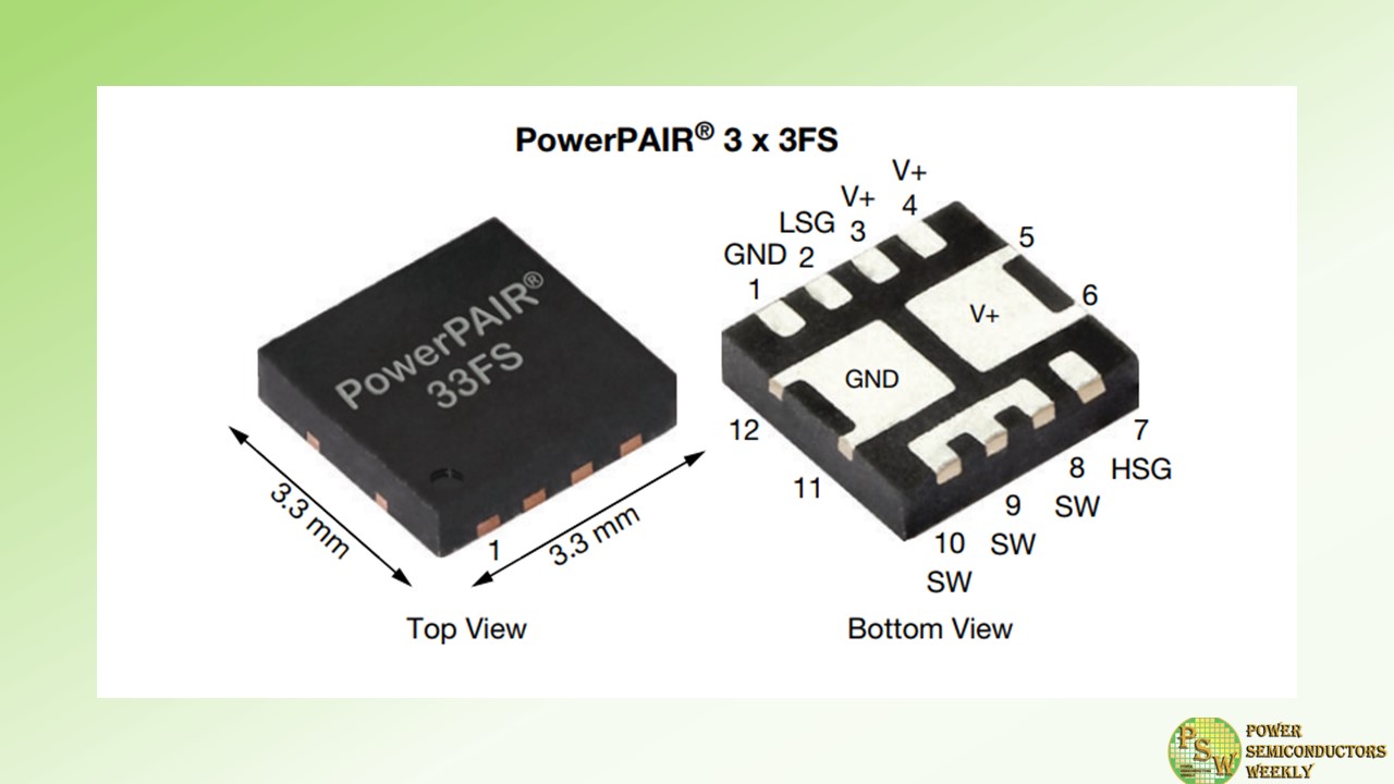
Vishay Intertechnology, Inc. introduced a new 80 V symmetric dual n-channel power MOSFET that combines high and low side TrenchFET® Gen IV MOSFETs in a single 3.3 mm by 3.3 mm PowerPAIR® 3x3FS package. For power conversion in industrial and telecom applications, the Vishay Siliconix SiZF4800LDT increases power density and efficiency, while enhancing thermal performance, reducing component counts, and simplifying designs.
This dual MOSFET can be used in place of two discrete devices typically specified in the PowerPAK 1212 package — saving 50 % board space. The device provides designers with a space-saving solution for synchronous buck converters, point of load (POL) converters, and half- and full-bridge power stages for DC/DC converters in radio base stations, industrial motor drives, welding equipment, and power tools. In these applications, the high and low side MOSFETs of the SiZF4800LDT form an optimized combination for 50 % duty cycles, while its logic level turn-on at 4.5 V simplifies circuit driving.
To increase power density, the MOSFET offers best in class on-resistance down to 18.5 mW typical at 4.5 V. This is 16 % lower than the closest competing device in the same package dimensions. For increased efficiency in high frequency switching applications, the SiZF4800LDT offers a low on-resistance times gate charge — a key figure of merit (FOM) for MOSFETs used in power conversion applications — of 131mW*nC and on-resistance times gain-drain charge
The device’s flip-chip technology enhances thermal dissipation — resulting in 54 % lower thermal resistance compared to competing MOSFETs. The SiZF4800LDT’s combination of low on-resistance and thermal resistance results in a continuous drain current of 36 A, which is 38 % higher than the closest competing device. The MOSFET features a unique pin configuration that enables a simplified PCB layout and supports shortened switching loops to minimize parasitic inductance. The SiZF4800LDT is 100 % Rg- and UIS-tested, RoHS-compliant, and halogen-free.
Competitor Comparison Table:
Part number SiZF4800LDT (New) Competitor SiZF4800LDTPerformance improved Package PowerPAIR 3x3FS PowerPAIR 3x3FS Dimensions (mm) 3.3 x 3.3 x 0.75 3.3 x 3.3 x 0.75 – Configuration Symmetric dual Symmetric dual – VDS (V) 80 80 – VGS (V) ± 20 ± 20 – RDS(on) (mΩ) @ 4.5 VGS Typ. 18.5 22 +16 % Max. 23.8 29 +18 % Qg (nC) @ 4.5 VGS Typ. 7.1 6.0 – FOM – 131 132 +1 % ID (A) Max. 36 26 +38 % RthJC (C/W) Max. 2.2 4.8 +54 % Original – Vishay Intertechnology
-

Vitesco Technologies is preparing the series application of its High Voltage Box. The modular system makes charging, converting and distributing electricity in electric vehicles cheaper by integrating several functions in one unit, depending on the design.
This includes the vehicle On-Board Charger for AC charging on the grid with up to 22 kW of charging power, a DC current converter providing the current for the 12 V vehicle net, and power electronics which distribute high voltage power in the vehicle and facilitate fast DC-charging with up to 800 V.
Owed to the high level of mechatronic integration, the High Voltage Box has smaller space requirements to the vehicle while increasing the total system reliability in comparison to individual devices. State-of-the art silicon carbide (SiC) semiconductors boost charging efficiency to over 95 percent which lowers the vehicle owner’s electricity bill. This efficiency level is particularly beneficial for car owners because electric vehicles are frequently charged on the grid.
Due to the high AC charging rate of up to 22 kW the High Voltage Box charges the car with 200 km of range in under two hours. DC high-power charging with up to 800 V achieves the same range in 12 minutes. The sophisticated power electronics ensure that this system offers electrical safety as well as efficiency.
On a day-to-day level, charging, energy conversion and power distribution are just as relevant for a driver’s satisfaction with a vehicle as driving itself is. With our High Voltage Box, we integrate these core tasks of energy management into one efficient and compact unit. This integration makes electrification on a large scale and at low cost easier.
Thomas Stierle, Member of the Executive Board and head of the Electrification Solutions division of Vitesco Technologies
Today, the so-called On-Board Charger (OBC) for charging with alternating current (AC) on the grid is a separate device in the vehicle. This OBC inverts grid power to direct current (DC) that can be fed to the high voltage battery. Another separate device is the DC/DC converter which provides direct current from the high voltage battery to the 12 V power net – or it boosts 12 V to high voltage DC. A power electronics unit distributes high voltage current within the vehicle (hence: Power Distribution Unit, PDU). In addition, these electronics can be designed to allow DC charging with up to 800 V at high power charging points. All those components need to be connected, they require a housing, installation space, and cooling.
The modular and scalable High Voltage Box makes it easier to cover two or more of these functions with a single device. SiC technology is used to minimize the conversion losses of the unit:
A high level of efficiency brings the car owner’s electricity bill down and contributes to sustainability.
Christian Preis, Head of Base Development Energy Transformation at Vitesco Technologies
Within the modular design Vitesco Technologies covers all relevant European and worldwide grid topologies. The High Voltage Box was developed to support modular vehicle adaptation for the global market. At the same time, Vitesco Technologies is driving new functions ahead. The High Voltage Box for one of the two series applications will already function bidirectionally so that it can supply alternating current with 230 V from the DC battery current when this is required.
This puts vehicle owners in the comfortable position to make versatile use of their large battery. For instance, if they wish to use power tools far away from the grid, or if they want to feed electricity to the grid which they have charged earlier from their own photovoltaic system. “In the future, this option to stabilize the grid will continue to gain importance “, Preis adds. The company’s experts are advancing the necessary standard for this in key committees and are thus part of the decision-making process about development trends.
In the future the High Voltage Box with bidirectional function can also make it possible to power a whole house from the High Voltage Battery during a blackout. This is an option because batteries in vehicles have a much bigger capacity than most of the batteries typically installed in private homes.
Original – Vitesco Technologies
-
Infineon Technologies AG introduced a new product family of Solid-State Isolators to achieve faster and more reliable circuit switching with protection features not available in optical-based solid state relays (SSR). The isolators use coreless transformer technology and support 20 times greater energy transfer with both current and temperature protection contributing to a higher reliability and lower cost of ownership.
The new solid-state isolators allow driving the gates of Infineon’s MOS-controlled power transistors OptiMOS ™ and CoolMOS™ to reduce power dissipation of up to 70 percent of todays’ solid-state relays using SCR (silicon-controlled rectifier) and Triac switches.
Infineon’s solid-state isolators enable custom solid-state relays capable of controlling loads more than 1000 V and 100 A. Improved performance and reliability make coreless transformer technology ideal for applications in advanced battery management, energy storage, renewable energy systems, as well as industrial and building automation system applications. With Infineon’s solid-state isolator drivers, engineers can further improve the efficiency of electronic and electromechanical systems.
“Implementing coreless transformers in solid-state isolators and relays is truly a game-changer for power engineers; it provides 50 times lower RDS (on) than existing optically controlled solutions. This enables their use in higher-voltage and higher power applications,” said Davide Giacomini, Marketing Director for the Green Industrial Power Division at Infineon Technologies.
When matched with Infineon’s CoolMOS S7 switch, the isolator drivers enable switching designs with a much lower resistance compared to optically driven solid-state solutions. This translates to longer lifespans and lower cost of ownership in system designs. As with all solid-state isolators, the devices also offer superior performance compared to electromagnetic relays, including 40 percent lower turn-on power and increased reliability due to elimination of moving parts.
The family of devices is designed to be compatible with Infineon’s broad switching portfolio including Infineon’s CoolMOS S7, OptiMOS TM and linear FET portfolios.
Original – Infineon Technologies
-

Toshiba Electronic Devices & Storage Corporation announced that it has started construction of a back-end production facility for power semiconductors at Himeji Operations – Semiconductor, in Hyogo Prefecture, western Japan. The new facility will start mass production in spring 2025.
Toshiba will promote smart factory initiatives that bring automated transportation systems into manufacturing processes, promote work efficiency through adoption of RFIDNote tags, and improve the accuracy of inventory management. The facility will be 100% powered by renewable energy and equipped with solar power generation systems, underlining Toshiba’s commitment to the SDGs.
Power devices are essential components for managing and reducing power consumption in all kinds of electronic equipment, and for saving energy. With the start of production at the new Himeji facility, Toshiba will more than double its production capacity for automotive power semiconductor production, against fiscal 2022, and reinforce its contributions to advancing carbon neutrality.
Original – Toshiba
