-

Cambridge GaN Devices (CGD) is addressing higher power industrial applications with its ICeGaN™ technology which has already proved itself rugged, reliable and easy-to-use in high volume consumer devices. At the APEC 2024, IEEE Applied Power Electronics Conference and Exposition, the company is introducing new reference designs and showing demos which address the broad and diverse industrial market.
Andrea Bricconi | Chief Commercial Officer, CGD
“We are acutely aware of the increasing power requirements of industrial applications, and the need for high efficiency. For example, as the use of Artificial Intelligence (AI) proliferates, the power demanded by the exponential growth in power demanded by datacentres is growing almost exponentially. Other applications, such as solar inverters, amplifiers, transport and smart mobility, process control and manufacturing are also interested in GaN and the feedback we have received is that they love the simplicity of our ‘Drive it Like a MOSFET’ approach.”
At APEC, visitors to the booth are able to see the progress that CGD is making to support both emerging and existing markets for GaN technology..
With a high power density of 23 W/in3, GGD’s 350 W PFC/LLC reference design has an average efficiency of 93%, and a no-load power consumption of 150 mW. The CrM Totem Pole PFC + Half-Bridge LLC PSU has been realised using CGD’s 650 V, 55 mΩ, H2 series ICeGaN technology, and delivers 20 V / 17.5 A output.
The result of a partnership deal struck last year with Neways Electronics, a 3 kW photo-voltaic inverter is used to boost the DC solar voltage to a stable DC link voltage. With a maximum efficiency of 99.22% due to zero-current switching, it is a perfect example of how CGD’s GaN HEMT structure is simple for engineers to use, since it employs a standard silicon controller from Analog Devices Inc.
ICeGaN has been employed by AGD Productions in its compact AGD DUET amplifier which is rated at 300W 4Ω. This is the first time the company has used a 100% GaN power transistor design for both the power stage and the amplifier.
Finally, the GaNext project, a consortium of 13 partners from three nations has delivered compact 1 kW intelligent power modules featuring integrated drive, voltage control and protection circuits using CGD’s ICeGaN.
Original – Cambridge GaN Devices
-
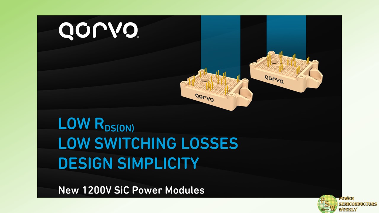
Qorvo® announced four 1200V silicon carbide (SiC) modules – two half-bridge and two full-bridge – in a compact E1B package with RDS(on) starting at 9.4mΩ. These highly efficient SiC modules are excellent solutions for electric vehicle (EV) charging stations, energy storage, industrial power supplies and solar power applications.
“The modules in this new family can replace as many as four discrete SiC FETs, thus simplifying thermomechanical design as well as assembly. Our cascode technology also allows higher switching frequency operation, further reducing solution size by using smaller external components,” said Ramanan Natarajan, director of product line marketing for Qorvo’s SiC Power Products business.
“For our customers, the high efficiency of these modules streamlines the power supply design process, so they can focus on the design, layout, assembly, characterization and qualification of one module as opposed to numerous discrete components.”
Led by the 9.4mΩ UHB100SC12E1BC3N, these four SiC modules leverage Qorvo’s unique cascode configuration, which minimizes RDS(on) and switching losses to maximize efficiency, especially in soft-switching applications. Silver-sinter die attach reduces thermal resistance to as low as 0.23 °C/W; when combined with the stacked die construction found in the “SC” part numbers, power cycling performance is improved by 2X over comparable SiC power modules on the market.
Together, these characteristics contribute to superior thermal performance and reliability with the ease of use and power density of a highly integrated SiC power module.
The table below provides a snapshot of Qorvo’s new 1200V SiC module family:
Part # Description RDS(on) @25C (mΩ) UFB15C12E1BC3N 1200V, 15A SiC full-bridge module 70 UFB25SC12E1BC3N 1200V, 25A SiC full-bridge module 35 UHB50SC12E1BC3N 1200V, 50A SiC half-bridge module 19 UHB100SC12E1BC3N 1200V, 100A SiC half-bridge module 9.4 Qorvo’s suite of powerful design tools like its FET-Jet Calculator and QSPICE™ software aid in product selection and performance simulation. For more information about Qorvo’s advanced SiC solutions for industrial applications, please visit www.qorvo.com/go/sic.
Original – Qorvo
-

Power Integrations announced the InnoMux™-2 family of single-stage, independently regulated multi-output offline power-supply ICs. InnoMux-2 ICs consolidate AC-DC and downstream DC-DC conversion stages into a single chip, providing up to three independently regulated outputs for use in white goods, industrial systems, displays and other applications requiring multiple voltages.
Elimination of separate DC-DC stages slashes component count, reduces PCB footprint and increases efficiency by as much as 10 percentage points compared to traditional two-stage architectures. Efficiency is aided by the ICs’ 750 V PowiGaN™ gallium-nitride transistors, zero-voltage switching (without an active clamp) and synchronous rectification.
Roland Saint-Pierre, vice president of product development at Power Integrations said: “Most modern electronic systems rely on multiple internal voltages to operate various functions such as computing, communication and actuation function – typically heat, light, sound or motion of some kind. But losses in each conversion stage are compounded, degrading system performance and generating heat.
The InnoMux-2 IC overcomes this challenge by providing up to three independently regulated voltage outputs or two voltage output and a constant current output from a single stage, achieving a compact and efficient power sub-system with low component count.”
InnoMux-2 ICs deliver up to 90 watts of output power with accurate regulation of better than ±3 percent across the full input line, load, temperature and differential current step conditions. Total power system efficiency (AC to regulated low-voltage DC segment) is above 90 percent; the advanced InnoMux-2 controller also manages light-load power delivery, avoiding the need for pre-load resistors and reducing no-load consumption to less than 30 mW. This conserves power for necessary functionality in applications subject to the 300 mW allowance for standby usage under the European energy-using product (EuP) regulations.
InnoMux-2 devices leverage Power Integrations’ thermally efficient InSOP™24 and InSOP™28 packages with PCB cooling, so no heatsink is required. Device options include dual- and three-output constant voltage (CV); optionally, one output may be dedicated to constant current (CC) drive, suitable for powering LEDs in displays or for high-speed charging of an internal battery. Typical applications include TVs, monitors, appliances, networking, home and building automation, LED emergency lighting and industrial power supplies.
Original – Power Integrations
-
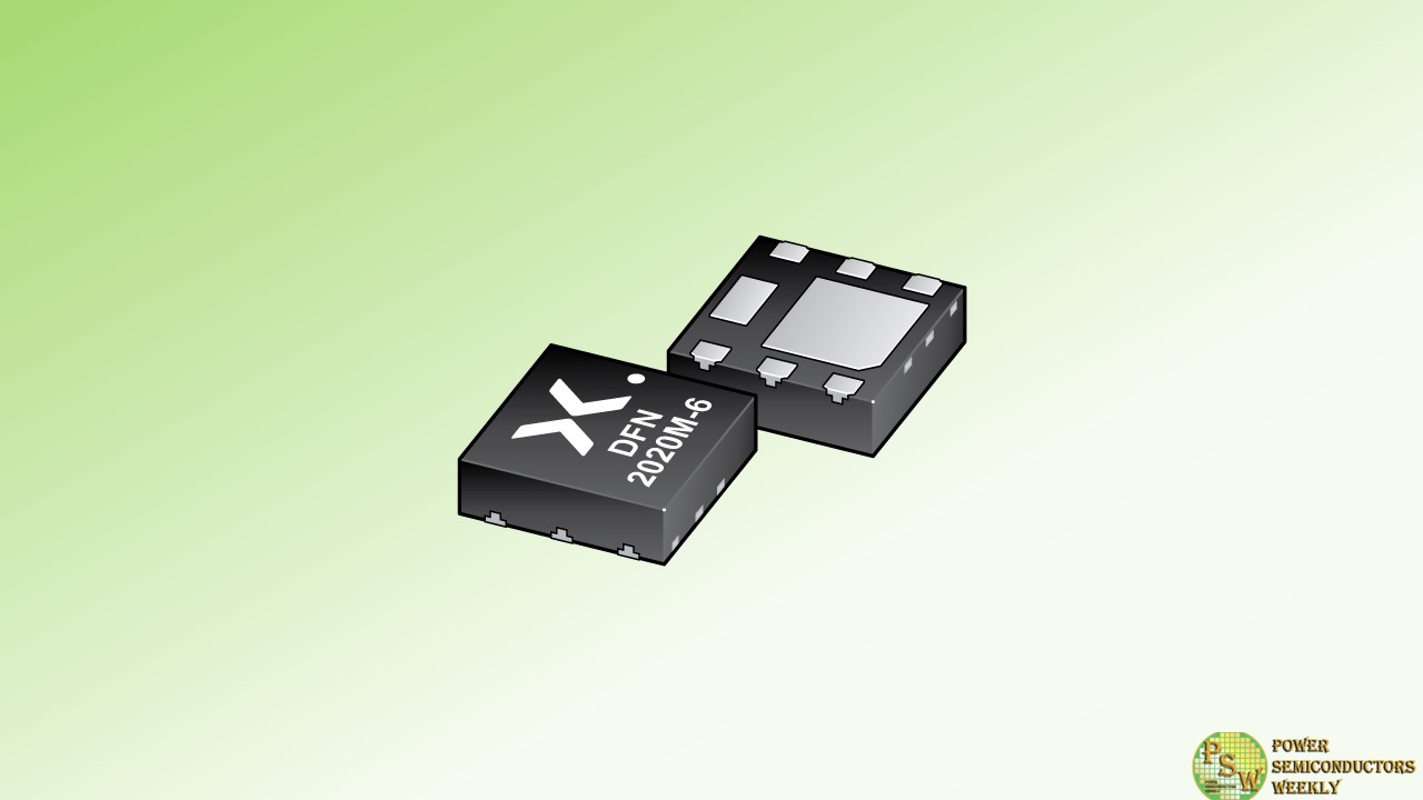
Nexperia is once again bringing its product innovations to APEC and today announced the release of several new MOSFETs to further broaden its range of discrete switching solutions for use in various applications across multiple end markets.
This release includes 100 V application specific MOSFETs (ASFETs) for PoE, eFuse and relay replacement in 60% smaller DFN2020 packaging, and 40 V NextPowerS3 MOSFETs with improved electromagnetic compatibility (EMC) performance.
PoE switches typically have up to 48 ports, each requiring 2 MOSFETs for protection. With up to 96 MOSFETs on a single PCB, any reduction in device footprint is attractive. For this reason, Nexperia has released 100 V PoE ASFETs in 2 mm x 2 mm DFN2020 packaging which occupies 60% less space than previous versions in LFPAK33 packaging.
A critical function of these devices is to protect PoE ports by limiting inrush currents while safely managing fault conditions. To manage this scenario, Nexperia has enhanced the safe operating area (SOA) of these devices by up to 3x with only a minimal increase in RDS(on). These ASFETs are also suitable for battery management, Wi-Fi hotspot, 5G picocell and CCTV applications and can serve as replacements for mechanical relays in smart thermostats, for example.
EMC-related issues caused by MOSFET switching usually only emerge late in the product development life cycle and resolving them can incur additional R&D costs and delay market release. Typical solutions include using significantly more expensive MOSFETs with lower RDS(on) (to slow down switching and absorb excessive voltage ringing) or to fit an external capacitive snubber circuit but this approach has the disadvantage of increasing component count.
Nexperia has optimized its 40 V NextPowerS3 MOSFETs to offer similar EMC performance as that which can be achieved using an external snubber circuit, while also offering higher efficiency. These MOSFETs are suitable for use in switching converters and motor controllers across various applications and are available in LFPAK56 packaging.
“By introducing these latest additions to our range of discrete FET solutions at APEC 2024, Nexperia showcases how we leverage our expertise in R&D to deliver optimized solutions. Both our new 100 V PoE ASFETs as well as improved EMC performance in our 40 V NextPowerS3 MOSFETs demonstrate our commitment to supporting engineers in overcoming challenges across diverse applications. These innovations underscore Nexperia’s dedication to providing efficient, compact, and reliable solutions that empower our customers to succeed in today’s ever-evolving market,” says Chris Boyce, MOSFET Marketing & Product Group Director at Nexperia.
Original – Nexperia
-
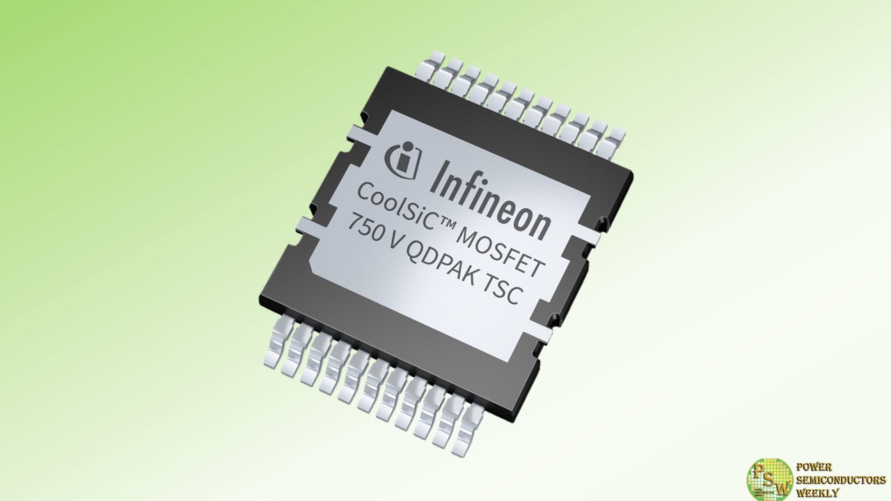
Infineon Technologies AG introduced the 750V G1 discrete CoolSiC™ MOSFET to meet the increasing demand for higher efficiency and power density in industrial and automotive power applications. The product family includes both industrial-graded and automotive-graded SiC MOSFETs that are optimized for totem-pole PFC, T-type, LLC/CLLC, dual active bridge (DAB), HERIC, buck/boost, and phase-shifted full bridge (PSFB) topologies.
The MOSFETs are ideal for use in both typical industrial applications, such as electric vehicle charging, industrial drives, solar and energy storage systems, solid state circuit breaker, UPS systems, servers/ datacenters, telecom, and in the automotive sector, such as onboard chargers (OBC), DC-DC converters, and many more.
The CoolSiC MOSFET 750 V G1 technology features excellent RDS (on) x Q fr and superior RDS (on) x Q oss Figure-of-Merits (FOMs), resulting in ultra-high efficiency in hard-switching and soft-switching topologies respectively. Its unique combination of high threshold voltage (V GS(th), Typ. of 4.3 V) with low Q GD/Q GS ratio ensures high robustness against parasitic turn-on and enables unipolar gate driving, leading to increased power density and low cost of the systems.
All devices use Infineon’s proprietary die-attach technology which delivers outstanding thermal impedance for equivalent die sizes. The highly reliable gate oxide design combined with Infineon’s qualification standards delivers robust and long-term performance.
With a granular portfolio ranging from 8 to 140 mΩ RDS (on) at 25°C, this new CoolSiC MOSFET 750 V G1 product family meets a wide range of needs. Its design ensures lower conduction and switching losses, boosting overall system efficiency.
Its innovative packages minimize thermal resistance, facilitate improved heat dissipation, and optimize in-circuit power loop inductance, thereby resulting in high power density and reduced system costs. It’s important to note that this product family features the cutting-edge QDPAK top-side cooled package.
Original – Infineon Technologies
-

GlobalWafers held its board meeting to approve 2023 financial results.
FY2023 consolidated revenue reached NT$70.7 billion with YoY 0.5%; gross profit of NT$26.4 billion, with -12.9% YoY, gross profit margin of 37.4%, with -5.8% YoY; operating income of NT$20.1 billion, with -19.7% YoY, operating income margin of 28.4%, with -7.1% YoY; profit before tax of NT$26.5 billion, with 31.8% YoY, profit before tax margin of 37.5%, with 8.9% YoY; net profit of NT$19.8 billion, with 28.6% YoY, net profit margin of 28.0%, with 6.1% YoY; EPS reached NT$45.41, with an increase of more than NT$10 compared with the previous year.
FY2023 consolidated revenue grew in 3 concessive years and rose to the highest again! FY2023 EPS, profit before tax margin and net profit margin all hit record high.
Despite the semiconductor industry in 2023 facing a slowdown in global economic and consumer electronics demand, coupled with increased inventory pressure, GlobalWafers benefited from a high proportion of LTAs and maintained high utilization rates for FZ wafers and compound semiconductor wafers, achieving continued growth in revenue throughout the year.
Looking ahead to 2024, as terminal market inventories are gradually reabsorbed, AI features will progressively integrate into personal computers, tablets, and smartphones, potentially driving a wave of upgrades. In the meantime, the AI ecosystem relies on supports from peripherals and semiconductor components, fueling demands for edge computing, high-performance computing (HPC) and spurring the development of low-power consumption-related components (SiC, ULLD, IGBT…).
More innovations are expected to be introduced, such as 5G, electrification, smart cockpits, and autonomous driving, contributing to the growth momentum in the semiconductor market. Besides, policies related to energy transition and net-zero carbon emissions in various countries have laid a long-term foundation for the development of compound semiconductors. In 2024, the market is expected to gradually recover, with memory leading the way in releasing signals.
However, the pace and extent of economic recovery depend on various factors, including different terminal applications and global economic uncertainties such as war, rising shipping costs, interest rate changes, and exchange rate fluctuations. Positioned in the upstream of the semiconductor industry, GlobalWafers anticipates a recovery a quarter or two later than downstream and expects a healthier performance in the second half of the year compared to the first half, considering that customers will prioritize depleting existing inventories.
With a comprehensive product spectrum ranging from 3” to 12” semiconductor wafers, GlobalWafers is able to cater for customers’ needs to cope with market fluctuations of individual products. Moreover, the Company has carried out expansion plans to get ready for the acceleration toward advanced processes.
GlobalWafers has become a long-term partner of customers with its focus on sustainability and the unique advantages of highly regionalized deployment that allows the Company to supply products in proximity, reducing the carbon footprint and the impact of carbon tariffs, while also mitigating geopolitical risks. With flexible asset allocation and a sound financial structure, GlobalWafers is resilient to market volatility and continues to create profits through prudent operations.
Original – GlobalWafers
-

EPC introduced the 100 V, 1 mOhm EPC2361. This is the lowest on-resistance GaN FET on the market offering double the power density compared to EPC’s prior-generation products.
The EPC2361 has a typical RDS(on) of just 1 mOhm in a thermally enhanced QFN package with exposed top and tiny, 3 mm x 5 mm, footprint. The maximum RDS(on) x Area of the EPC2361 is 15 mΩ*mm2 – over five times smaller than comparable 100 V silicon MOSFETs.
With its ultra-low on-resistance, the EPC2361 enables higher power density and efficiency in power conversion systems, leading to reduced energy consumption and heat dissipation. This breakthrough is particularly significant for applications such as high-power PSU AC-DC synchronous rectification, high frequency DC-DC conversion for data centers, motor drives for eMobility, robotics, drones, and solar MPPTs.
“Our new 1 mΩ GaN FET continues to push the boundaries of what is possible with GaN technology, empowering our customers to create more efficient, compact, and reliable power electronics systems,” comments Alex Lidow, EPC CEO and co-founder.
Original – Efficient Power Conversion
-

Arrow Electronics, Inc. and its engineering services company, eInfochips, are working with Infineon Technologies AG to help eInfochips’ customers accelerate the development of electric vehicle (EV) chargers.
Development of EV chargers, especially DC “fast chargers,” is becoming increasingly challenging to equipment manufacturers due to several factors, such as lack of prior experience, stringent functional safety and reliability requirements, and a fledgling support network. The collaboration between Arrow and Infineon aims to help innovators navigate these challenges while accelerating time-to-market.
As part of the collaboration, Arrow’s High Power Center of Excellence has developed a 30kW DC fast charger reference platform. This includes Infineon’s 1200V CoolSiC™ Easy power modules and also hardware design, embedded firmware, bi-directional charging support and energy metering functionality.
“Combining Arrow’s strength in components, engineering and design services with Infineon’s innovative products will help customers accelerate their design and speed to market in e-mobility applications,” said Murdoch Fitzgerald, vice president, global engineering and design services at Arrow. “Customers can rely on this collaboration to deliver innovative and leading edge DC faster chargers, accelerate and de-risk design cycles, and get access to a world-class support team enabling them to plan and manage their product roadmap and lifecycles.”
“Infineon is on a drive towards decarbonization and digitalization with our ecosystem partners, and this collaboration with Arrow is a testament to this mission,” said Shri Joshi, vice president of Green Industrial Power, Infineon Technologies Americas. “The joint 30kW DC fast charger reference platform, which includes Infineon’s latest power modules and devices, will help our customers bring more fast chargers to market as the future moves to electrical vehicles. We look forward to this ongoing collaboration to support our customer base.”
The first reference design from this collaboration, a production-grade 30kW DC fast charger reference development platform, is being demonstrated at Applied Power Electronics Conference, Feb. 25-29, in Long Beach, Calif.
Original – Arrow Electronics
-

Vishay Intertechnology, Inc. announced that at the Applied Power Electronics Conference and Exposition (APEC) 2024, the company is showcasing its broad portfolio of passive and semiconductor solutions that address the latest trends in power electronics — from energy harvesting, electric vehicle (EV) powertrains, and mass commercialization to efficient and effective power electronics for power tools and switching regulators that shorten the iterative design cycle.
Taking center stage in booth 1607 will be Vishay’s newly released 1200 V MaxSiC™ series silicon carbide (SiC) MOSFETs, which deliver on-resistances of 40, 80 and 250 mΩ in standard packages for industrial applications, with custom products also available. In addition, Vishay will provide a roadmap for 650 V to 1700 V SiC MOSFETs with on-resistances ranging from 12 mΩ to 1 Ω.
Vishay’s SiC platform is based on a proprietary MOSFET technology — enabled through the company’s recent acquisition of MaxPower Semiconductor, Inc. — which will address market demands in traction inverter, photovoltaic energy storage, on-board charger, and charging station applications. At the booth, Vishay’s experts will also be discussing upcoming planned releases of the MaxSiC platform, including AEC-Q101 Automotive Grade products.
At APEC 2024, Vishay will also be offering a variety of product-focused demonstrations highlighting IHPT haptic actuators; the THJP ThermaWick® Thermal Jumper; the pulse performance of MELF, CRCW / CRCW-HP thick film, and MCS, MCU, and MCW thin film chip resistors; and the thermal capabilities of the PCAN and RCP high power thin and thick film resistors. In addition, application-focused demonstrations will include:
- An 800 V SiC MOSFET heat pump with a 100 % Vishay BOM
- A high voltage intelligent battery shunt for 400 V and 800 V batteries
- A six-phase DC/DC converter for mild hybrid vehicles with 48 V boardnets that provides power to 12 V loads up to 3 kW with high efficiency to 97 %
- A semiconductor-based, resettable eFuse for 800 V electric vehicle systems
Additional Vishay passive components on display at APEC 2024 will include the IHDM series of high current, edge-wound through hole inductors with continuous operation to +180 °C; hybrid planar and integrated transformers; wireless charging coils; NTC thermistors and PTC thermistors, including the PTCEL series capable of handling energy absorption up to 240 J; high power wirewound, thin film, and thick film resistors, including the anti-surge RCS with power to 0.5 W in the 0805 case size; high voltage thick film resistors and dividers; high voltage aluminum, ceramic, and power electronic capacitors (PEC); high energy tantalum capacitors; and robust metallized polypropylene film capacitors, including the MKP1848e DC-Link capacitor with high temperature operation to +125 °C.
Highlighted Vishay semiconductor solutions will consist of the SiC967 high voltage synchronous buck regulator with integrated power MOSFETs and inductors; 400 V, 600 V, and 1200 V standard rectifiers in SlimDPAK 2L and SMPD 2L packages with high creepage distance; 650 V and 1200 V SiC Schottky diodes up to 12 A in eSMP® series and power packages for AC/DC power factor correction (PFC) and ultra high frequency output rectification; and transient voltage suppressors (TVS).
Original – Vishay Intertechnology
-
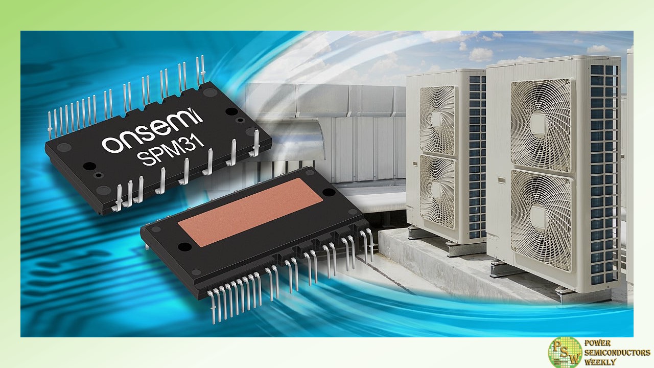
onsemi announced the availability of its 1200V SPM31 Intelligent Power Modules (IPMs) featuring the latest generation Field Stop 7 (FS7) Insulated Gate Bipolar Transistor (IGBT) technology. The SPM31 IPMs deliver higher efficiency, smaller footprint and higher power density resulting in lower total system cost than other leading solutions on the market.
Given the greater efficiency realized using optimized IGBTs, these IPMs are ideal for three-phase inverter drive applications such as heat pumps, commercial HVAC systems, servo motors, and industrial pumps and fans.
Operating residential and commercial buildings is estimated to contribute 26% of greenhouse gas emissions, with indirect emissions such as heating, cooling and powering buildings accounting for approximately 18%. As governments worldwide strive to meet their energy and climate commitments, more energy-efficient and lower-carbon solutions are becoming increasingly critical.
The SPM31 IPMs control the power flow to the inverter compressor and fans in heat pumps and air conditioning systems by adjusting the frequency and voltage of the power supplied to three-phase motors for maximum efficiency. For example, onsemi’s 25A-rated SPM31 using FS7 IGBT technology can decrease power losses by up to 10% and increase in power density up to 9%, compared to our previous generation products.
With the transition to electrification and heightened efficiency mandates, these modules help manufacturers drastically improve system design while increasing efficiency in heating and cooling applications. With the improved performance, our SPM31 IPM family featuring FS7 enables high efficiency with reduced energy losses, further reducing harmful emissions globally.
These highly integrated modules contain gate-driving ICs, multiple on-module protection features along with our FS7 IGBTs enabling industry-leading thermal performance with the ability to support a wide range of currents, from 15A to 35A. With their best-in-class power density, SPM31 FS7 IGBT IPMs are an ideal answer to save mounting space and improve performance expectations while shortening the development time. In addition, the SPM31 IPMs include the following benefits:
- Controls for gate drivers and protections
- Low loss, short-circuit-rated IGBTs
- Negative IGBT terminals available for each phase to support a wide variety of control algorithms
- Built-in under-voltage protection (UVP)
- Built-in bootstrap diodes and resistors
- Built-in high-speed high-voltage integrated circuit
- Single-grounded power supply
Original – onsemi
