-

EPC Space announced a distribution agreement with Avnet, a global distributor of electronic components and services. Avnet will be a global distributor for EPC Space’s line of radiation hardened (Rad Hard) GaN power devices qualified for satellite and high-reliability applications.
EPC Space offers a family of Rad Hard power GaN devices that includes discrete transistors, Integrated Circuits (ICs), and Modules that offer significant performance advantages over competitive silicon-based space level power devices. EPC Space’s GaN technology devices are smaller, have lower resistance, and have superior switching performance compared to silicon-based components and solutions.
Critical spaceborne applications that benefit from the performance improvements that EPC Space devices offer include satellite’s DC-DC converters, reaction and momentum wheels, solar array drive assembly, micro-pumps for propulsion systems, and more.
“Partnering with Avnet, a global leader in distribution solutions, allows EPC Space to offer timely and reliable service to customers seeking high reliability GaN power solutions,” said Bel Lazar, EPC Space’s CEO.
Original – EPC Space
-

STMicroelectronics introduced 100V trench Schottky rectifier diodes that boost efficiency in power converters operated at high switching frequencies.
Raising power-converter operating frequency, encouraged by the minimal switching losses of technologies like wide-bandgap semiconductors, allows designers to set new benchmarks in power density. However, at elevated frequencies, the energy losses in conventional planar diodes, including silicon Schottky devices, used as rectifiers become a significant factor limiting conversion efficiency.
ST’s trench Schottky diodes significantly reduce the rectifier losses, with superior forward-voltage and reverse-recovery characteristics that enable increased power density with high efficiency. The forward voltage is 50-100mV better than in comparable planar diodes, depending on current and temperature conditions. Simply changing to these devices can increase the efficiency by 0.5%.
There are 28 variants in the new family, with eight current ratings from 1A to 15A, multiple surface-mount packages, in industrial and automotive grades. The industrial-grade parts target applications such as miniature switched-mode power supplies and auxiliary power supplies for telecom, server, and smart-metering equipment.
In automotive, typical uses include space-constrained applications such as LED lighting, reverse-polarity protection, and low-voltage DC/DC converters. The parts are AEC-Q101 qualified, manufactured in PPAP-capable facilities, and specified from -40°C to 175°C.
When combined with ST’s flyback and buck-boost converters, such as the VIPer controllers and HVLED001A offline LED driver, the 100V trench Schottky rectifiers fulfil the active-components bill of materials for switched-mode power supplies. All are supported in ST’s eDesign Suite Rectifier Diodes Simulator, which helps to select the rating and footprint, simulate waveforms, and estimate power efficiency.
The diodes are 100% avalanche tested in production to ensure device robustness and system reliability. They are available in DPAK as well as SOD123 Flat, SOD128 Flat, SMB Flat, and PSMC (TO227A) surface-mount packages.
Original – STMicroelectronics
-
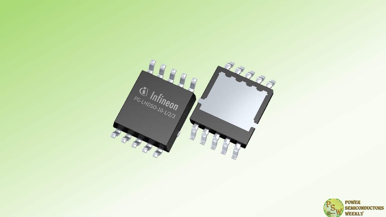
Infineon Technologies AG introduced the SSO10T TSC package with OptiMOS™ MOSFET technology. With its direct top-side cooling concept, the package offers excellent thermal performance. This eliminates heat transfer into or through the PCB of the automotive electronic control unit.
The package enables a simple and compact double-sided PCB design and minimizes cooling requirements and system costs for future automotive power designs. The SSO10T TSC is therefore well suited for applications such as electric power steering (EPS), EMB, power distribution, brushless DC drives (BLDC), safety switches, reverse battery, and DCDC converters.
The SSO10T TSC has a 5 x 7 mm² footprint and is based on the established industry standard SSO8, a 5 x 6 mm² robust housing. However, due to its top-side cooling, the SSO10 TSC offers more than 20 percent and up to 50 percent higher performance than the standard SSO8 – depending on the thermal interface (TIM) material used and the TIM thickness. The SSO10T TSC package is JEDEC listed for open market and provides wide second source compatibility. As a result, the package can be introduced quickly and easily as the future standard for top-side cooling.
The SSO10T package enables a very compact PCB design and reduces the system footprint. It also lowers the cost of the cooling design by eliminating vias, resulting in lower overall system costs and design effort. At the same time, the housing offers high power density and efficiency, thus supporting the development of future-proof and sustainable vehicles.
Original – Infineon Technologies
-

Alpha and Omega Semiconductor Limited announced its AONZ66412 XSPairFET™ MOSFET designed for Buck-Boost converters in USB PD 3.1 Extended Power Range (EPR) applications. The USB PD 3.1 EPR increases the USB-C maximum power up to 240W. AONZ66412 is defined to support the most commonly addressed power range of up to 140W at 28V, with two 40V N-Channel MOSFETs in a half-bridge configuration in a symmetric XSPairFET™ 5mmx6mm package.
The AONZ66412 can replace two single DFN5x6 MOSFETs, reducing the PCB area and simplifying the layout of the 4-switch buck-boost architecture while enabling a higher efficiency design. These benefits make the AONZ66412 ideal for buck-boost converters in Type-C USB 3.1 EPR applications, including notebook, USB hub, and power bank designs. The AONZ66412 is an extension to the AOS XSPairFET™ lineup that features the latest bottom source packaging technology and lower parasitic inductance for reduced switch node ringing.
Engineered with integrated high-side and low-side MOSFETs (3.8mOhms maximum on-resistance for each FET) within a DFN5x6 symmetric XSPairFET™ package, the low-side MOSFET source of the AONZ66412 is connected directly to a large paddle on the lead frame. This allows for improved thermals, as this paddle can be directly connected to the ground plane on the PCB. The improved package parasitics make 1MHz operation achievable, allowing inductor size and height to be reduced. AONZ66412 has been tested to achieve 97% efficiency @1MHz in typical USB PD 3.1 EPR conditions of 28V input, 17.6V output, and 8A load conditions.
“AOS specifically designed the AONZ66412 to meet EPR Type C PD application demands. AONZ66412 will reduce board space and improve power density to achieve the high-efficiency performance goals designers have set for this widely adopted USB-PD Type C application. AOS continues to be a leading innovator of buck-boost architecture solutions,” said Rack Tsai, Marketing Director of MOSFET product line at AOS.
Original – Alpha and Omega Semiconductor
-

Wolfspeed, Inc. hosted Senator Thom Tillis (R-NC) and other local officials, community partners, and employees at a ceremony to celebrate the topping out of construction at the $5 billion John Palmour Manufacturing Center for Silicon Carbide. Located in Chatham County, North Carolina, the JP will produce 200mm silicon carbide wafers, significantly expanding Wolfspeed’s materials capacity, and meet the demand for next generation semiconductors critical to the energy transition and AI.
“We are excited to mark this critical milestone alongside our hard-working team, loyal customers, community partners, and ardent supporters like Senator Thom Tillis,” said Wolfspeed President and CEO, Gregg Lowe.
“This facility is a testament to Wolfspeed’s commitment to our local community and domestic workforce, furthering our position as the global leader in silicon carbide production. The JP will help maintain America’s lead in energy innovation, and unlock significant benefits for our local community by growing the state’s economy by more than $17.5 billion over the next two decades and creating 1,800 good-paying jobs by 2030.”
“Wolfspeed’s $5 billion investment in Chatham County is another example of why North Carolina is the best state in the country to do business,” said Senator Tillis. “I was proud to vote in favor of the CHIPS and Science Act, which provides critical support for domestic semiconductor manufacturing, and I applaud Wolfspeed’s commitment to developing technology here in North Carolina that supports our national security and economic interests.”
The JP represents a total investment of $5 billion, complemented by public and private support, to help accelerate the transition from silicon to silicon carbide and ramp up supply of this material recently deemed as critical to the energy transition by the U.S. Department of Energy. By the end of 2024, phase one of construction is expected to be completed on the 445-acre site.
The ramp of the JP will support recently signed customer agreements with Renesas, Infineon, and additional companies, while driving meaningful progress towards Wolfspeed’s long-term growth strategy. The JP will primarily produce 200mm silicon carbide wafers, which are 1.7x larger than 150mm wafers, translating to more efficient wafers and ultimately, lower costs. The JP underpins Wolfspeed’s vision of accelerating the adoption of silicon carbide semiconductors across a wide array of end-markets and unlocking a new era of energy efficiency.
Wolfspeed currently produces more than 60% of the world’s silicon carbide materials at its Durham, N.C. headquarters, and is engaged in a $6.5 billion capacity expansion effort to dramatically increase production.
Original – Wolfspeed
-
Abstract
In this paper, a novel asymmetric trench SiC MOSFET with a Poly-Si/SiC heterojunction diode (HJD-ATMOS) is designed to improve its reverse conduction characteristics and switching performance. This structure features an integrated heterojunction diode, which improves body diode characteristics without affecting device static characteristics.
The heterojunction diode acts as a freewheeling diode during reverse conduction, reducing the cut-in voltage (Vcut-in) to a lower level than conventional asymmetric trench SiC MOSFET (C-ATMOS), while maintaining a similar breakdown voltage. Meanwhile, the split gate structure reduces gate-to-drain charge (Qgd). Through TCAD simulation, the HJD-ATMOS decreases Vcut-in by 53.04% compared to the C-ATMOS. Both Qgd and switching loss are reduced, with a decrease of 31.91% in Qgd and 40.29% in switching loss.
1. Introduction
The wide bandgap semiconductor properties of silicon carbide (SiC) make it a promising candidate for the development of future power switching devices. This is primarily due to SiC possessing properties such as a strong breakdown field, high physical and chemical stability, high thermal conductivity, and high electron saturation velocity.
SiC devices can operate in harsh environments due to their wide band gap of 3.25 eV and high thermal conductivity of 5 W/(cm·K). The SiC MOSFET is the most significant SiC power switching device due to its lack of trail current. This reduces switching loss and radiator volume, improving system power density.
SiC MOSFETs commonly make use of parasitic body-PN diodes as freewheeling diodes (FWD) in power inverter and converter systems. However, parasitic body-PN diodes in SiC MOSFETs are not ideal for use as freewheeling diodes. The reasons for this are as follows: Stacking faults (SFs) in SiC devices may cause reliability issues and increase conduction loss.
Although recent papers concerning the measured degradation of SiC MOSFETs show a high level of current threshold (about 5× the nominal current or more than 1000 A/cm2) for the starting of bipolar degradation, bipolar degradation effects can still occur in SiC MOSFETs under large cyclic pulse current densities. This will limit the application of SiC MOSFET devices in key areas, such as the surge current that flows through a diode during the start-up of a power converter, which can be more than ten times its rated current.
Furthermore, the body diode’s Vcut-in voltage (~2.7 V) is much higher than that of its silicon counterparts due to SiC’s wide bandgap. To overcome the drawbacks of parasitic body-PN diodes, numerous approaches have been devised to deactivate them. One approach is to integrate SiC MOSFETs with Schottky barrier diodes (SBDs). However, the use of external diodes not only introduces parasitic inductance, limiting switching frequency, but also consumes additional area in the package. And Schottky contacts suffer from a significant increase in reverse leakage current at high temperatures.
Furthermore, SiC MOSFETs with low-barrier and heterojunction diodes are available. Heterojunction diodes formed between polysilicon and SiC are attractive. Shenoy and Baliga, and Yamagami et al. presented studies on heterojunction diodes using P-Poly-Si and n-6H-SiC, and Poly-Si and 4H-SiC, respectively.
Both studies demonstrated low-forward-voltage Schottky-like characteristics. Ni et al. proposed a trench SiC MOSFET integrating polysilicon/SiC HJD, exhibiting excellent freewheeling diode (FWD) performance in both the first and third quadrants. The HJD’s unipolar behavior, similar to that of a Schottky diode, effectively suppresses the turn-on of the problematic body diode, mitigating the aging degradation observed in conventional SiC MOSFETs.
Additionally, HJDs reduce reverse recovery voltage and losses, enhancing long-term operational reliability. Furthermore, HJD integration eliminates the need for a separate SBD, leading to a smaller chip area, simpler packaging, and reduced overall system cost. This also minimizes parasitic inductance arising from additional components.
A novel asymmetric trench SiC MOSFET with a heterojunction diode at the right of the gate trench is proposed and simulated in this paper. The structure includes a trench gate with split-gate electrodes and a thicker P-Poly-Si layer, resulting in reduced gate charge and improved switching performance. To suppress the depletion layer, an n-type doped current spreading layer (N-CSL) is formed under the entire P-well region.
To maintain the breakdown voltage (BV) of the device structure while maintaining transfer and output characteristics similar to those of C-ATMOS, the depth of the P-well on the right side is not changed. The N-channel (Nch) is positioned below the P-Poly-Si and in contact with the CSL. The integrated HJD structure of the proposed device eliminates the requirement for an anti-parallel SiC SBD during reverse conduction. The HJD turns on at a low source–drain voltage (Vsd), thus eliminating bipolar degradation by inactivating the body diode. The split gate results in a decrease in gate charge, leading to a reduction in switching losses in the HJD-ATMOS without affecting other characteristics.
2. Device Structure and Mechanism
The schematic cross section of HJD-ATMOS and C-ATMOS is shown in Figure 1. Similar to C-ATMOS, the device forms an inversion layer channel in the first quadrant to facilitate electron conduction. The N-CSL layer on the N-drift region reduces the on-resistance. Deep P-wells are used to reduce the electric field stress in the gate oxide at the trench bottom and corner.
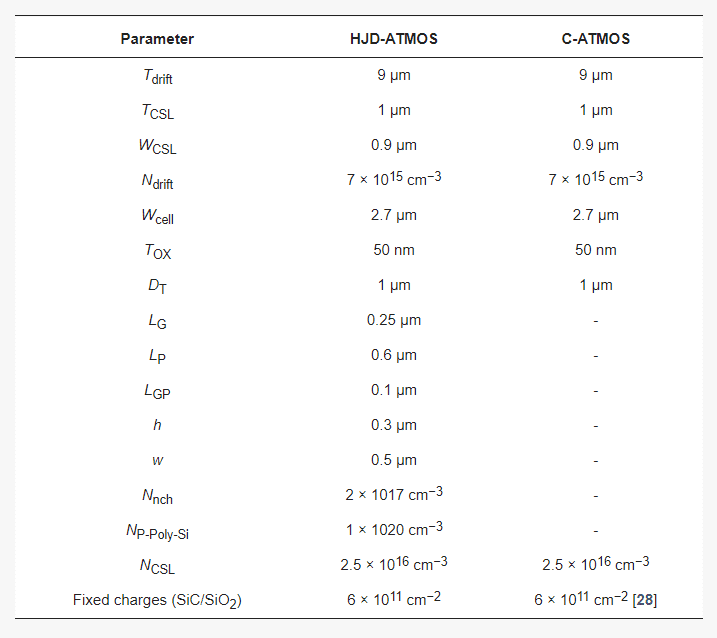
The primary distinction is the body diode structure. The Nch region under the P-Poly-Si provides a low-barrier path for electrons. Meanwhile, the HJD-ATMOS has a split gate and HJD structure on the right of the gate oxide layer. The split gate structure uses only a portion of the trench space for the gate electrode, while the other part is thicker P-Poly-Si that forms a portion of the HJD structure. The HJD-TMOS facilitates low-voltage conduction by allowing electrons to cross the lower heterojunction barrier in the third quadrant. The structure of Nch and N-channel doping concentration (Nnch) will be further discussed based on this optimization in this paper. Device specifications are presented in Table 1.
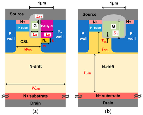
Figure 1. Schematic cross section of (a) HJD-ATMOS and (b) C-ATMOS.
Table 1. Main parameters used in the simulation.
Sentaurus TCAD simulations are used to analyze the performances of the HJD-ATMOS and the C-ATMOS, considering doping and temperature-dependent Shockley–Read–Hall and Auger recombination, doping-dependent transport, impact ionization, band narrowing, high-field velocity saturation, and mobility degradation, as well as fixed charges at the SiC/SiO2 interface for closer simulation results to experimental data.
The energy band diagram of the P-Poly-Si/N-SiC heterojunction at thermal equilibrium is shown in Figure 2b. The energy band diagram at thermal equilibrium along the A-A’ cut-line is shown in Figure 2a. The heterojunction has a conduction energy gap of 0.46 eV and a valence barrier energy gap of 1.78 eV. The electron barrier height ΦBN is determined by the Fermi level energy Ef and the conduction band peak energy Ec, which is about 1.39 eV.
Figure 2c shows the simulated carrier density at the heterojunction interface under forward bias at the rated voltage. Electrons are injected from N-SiC to P-poly, but there are few holes from P-poly to N-SiC due to the high hole barrier. Therefore, the HJD exhibits unipolar action, similar to the SBD.
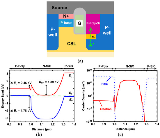
Figure 2. (a) Schematic cross section of HJD-ATMOS; (b) energy band diagram at thermal equilibrium along the A-A’ cut-line; (c) carrier density of the HJD when forward biased at rated voltage.
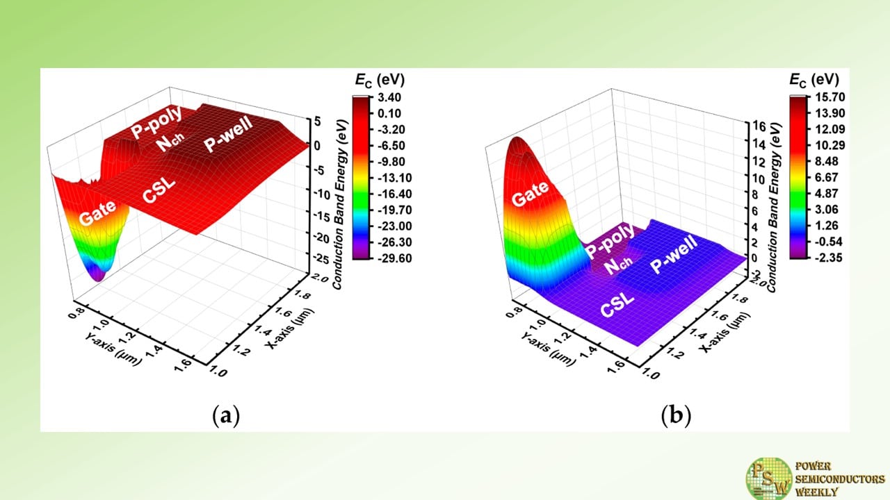
We also constructed a 3D band diagram of the device to better observe the working state of the device. Figure 3a shows the 3-D conduction band energy distribution of the device at Vds = 10 V and Vgs = 15 V. The band energy of Nch is higher than that of N-CSL, which prevents electron current from flowing to P-poly and enables the device to work normally like C-ATMOS.
Figure 3b shows the distribution of the devices when Vds = −5 V and Vgs = −5 V. The band energy of Nch is lower than that of N-CSL, resulting in electron current flowing from N-CSL to P-poly and preventing the turn-on of parasitic body-PN diodes.
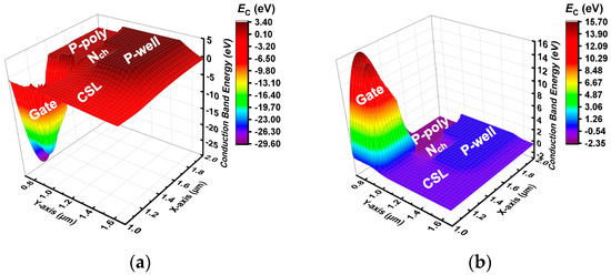
Figure 3. Three-dimensional conduction band energy distribution between P-poly, gate, Nch, N-CSL, and P-well (a) when conduction is forward and (b) when conduction is reverse.
Figure 4 shows the distribution of the total current density, hole current density, and electron current density of the device. From the total current density distribution, it can be seen that the current does not flow from P-Poly-Si to P-well. But a high current density is also noted at the gate corner of P-Poly-Si, which should be noted in use. From the hole current density distribution, it can be seen that holes do not enter N-drift.
This is due to the difference in the band gap between SiC and polysilicon. Since the energy barrier height between the SiC and polysilicon junctions in the valence band is very large, in the HJD-ATMOS, electron current can move toward the source while hole current cannot move toward the drain. The device can operate normally at electron current densities of 10 A/cm2 and 500 A/cm2.
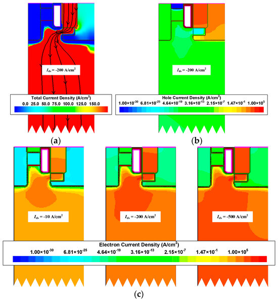
Figure 4. (a) Total current density distribution, (b) hole current density distribution, and (c) electron current density distribution at low and high current in the reverse conduction.
Figure 5 shows the I–V curves of HJD-ATMOS and C-ATMOS in forward and reverse conduction at room temperature. The steeper slope of the I–V curve of HJD-ATMOS in the first quadrant indicates that its specific on-resistance (Ron,sp) is lower than that of C-ATMOS. This is because the presence of Nch in HJD-ATMOS results in a smaller depletion region of P-well on N-CSL, leading to a wider current conduction region.
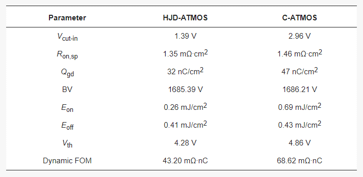
According to the calculations, at Vgs = 15 V and Ids = 200 A/cm2, the Ron,sp values for HJD-ATMOS and C-ATMOS are 1.35 mΩ∙cm2 and 1.46 mΩ∙cm2, respectively. In the third quadrant, at Ids= −10 A/cm2, HJD-TMOS exhibits a significantly lower Vcut-in of only 1.39 V compared to the PN diode of C-TMOS. As a result, HJD-ATMOS is capable of reducing switching losses.
The rated operating current of the device in the third quadrant is generally Ids = −200 A/cm2. This means that the proposed HJD-ATMOS has a clear advantage over C-ATMOS in that it can start working at a lower voltage. The hole density distribution diagram in Figure 5 for Ids = −200 A/cm2 shows that the integrated HJD effectively suppresses minority carrier injection, reducing bipolar degradation.
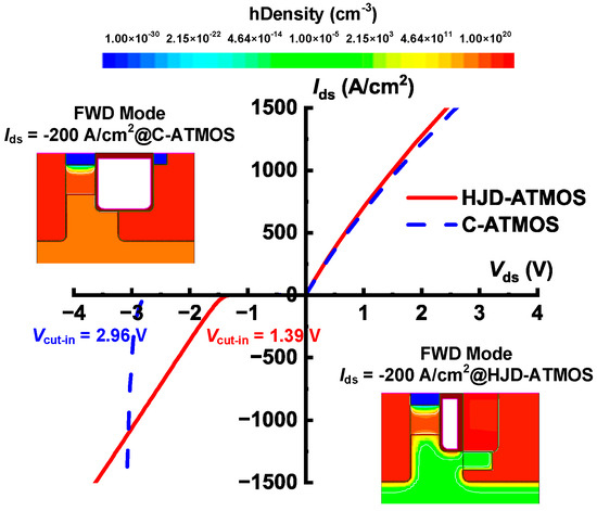
Figure 5. First and third quadrant characteristics of HJD-ATMOS and C-ATMOS.
In Figure 6, the local magnification shows that the HJD-ATMOS is affected by current spikes due to leakage. The figure demonstrates the change in breakdown voltage as a function of h and w when Nnch is, respectively, 2 × 1017 cm−3 and 2.5 × 1017 cm−3. It can be observed that when Nnch is 2.5 × 1017 cm−3, with h at 0.25 μm and w at 0.5 μm, the spike in the current is large, indicating the occurrence of leakage. When Nnch is 2.5 × 1017 cm−3, increasing h to 0.30 μm and w to 0.4 μm also results in leakage.
However, when Nnch is 2.0 × 1017 cm−3 and h increases to 0.3 μm, the device does not exhibit leakage, demonstrating that variations in Nnch have a significant impact on device performance. As shown in Figure 7, Vcut-in varies significantly with h. The minimum point of Vcut-in is 1.31 V at Nnch = 2 × 1017 cm−3, which is lower compared to its value of 1.71 V at Nnch = 2.5 × 1017 cm−3 and h = 0.2 μm.
This point represents the critical condition for the device not exhibiting leakage when Nnch = 2.5 × 1017 cm−3. After h is greater than 0.25 μm, the variation in Vcut-in with h tends to be flat, and if the value of h is larger, the protective effect of P-well on the gate oxide will also be weakened, and it will also increase the difficulty of process manufacturing.
As can be seen from Figure 8, when the device Vds is 0 V, Nnch is 2.5 × 1017 cm−3, and h is 0.25 μm, the HJD-ATMOS has more leakage than the device with Nnch is 2.0 × 1017 cm−3 and h is 0.30 μm. The darker regions in the current density plot for the HJD-ATMOS with Nnch at 2.5 × 1017 cm−3 and h at 0.25 μm are larger than those with Nnch at 2.0 × 1017 cm−3 and h at 0.30 μm, indicating higher leakage currents. This also confirms the hypothesis that the breakdown voltage spike is caused by heterojunction leakage. So the results indicate that Nnch = 2 × 1017 cm−3, h = 0.3 μm, and w = 0.5 μm are the optimal values.
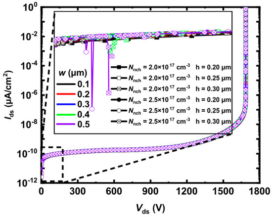
Figure 6. The breakdown voltage varies with h, w, and Nnch, when Nnch is 2.0 × 1017 cm−3 and 2.5 × 1017 cm−3, h is 0.20 μm, 0.25 μm and 0.30 μm, and w is 0.1 μm to 0.5 μm, respectively.
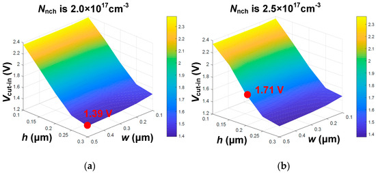
Figure 7. Vcut-in varies with h, w, and Nnch, when Nnch is (a) 2.0 × 1017 cm−3, and (b) 2.5 × 1017 cm−3.
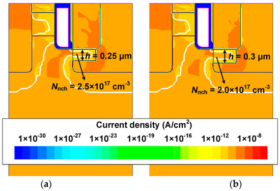
Figure 8. Current density distribution when (a) Nnch is 2.5 × 1017 cm−3, h is 0.25 μm, and (b) Nnch is 2.0 × 1017 cm−3, h is 0.30 μm at Vds = 0 V.
3. Simulation Results and Discussion
Figure 9 shows the capacitances of HJD-ATMOS and C-ATMOS. Gate voltage was fixed at 0 V, a 1 MHz AC signal was applied, and drain voltage was swept from 0 to 1000 V. HJD-ATMOS has lower gate-to-source capacitance (Cgs) than C-ATMOS due to the smaller contact area with the source caused by the split gate structure. HJD-ATMOS’s gate-to-drain capacitance (Cgd) does not decrease.
This is because the P-well blocks the right side of the gate of C-ATMOS, performing a similar function as the split gate. Therefore, it can be observed that the Ciss (Cgs + Cgd) of the HJD-ATMOS with split gates is also smaller than that of the C-ATMOS.
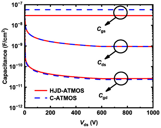
Figure 9. The device capacitance of HJD-ATMOS and C-ATMOS.
Gate-to-drain charge (Qgd) is critical for power device switching speed in device applications. Figure 10 shows a test circuit to simulate HJD-ATMOS and C-ATMOS gate charges during turn-on. The miller plateau height of HJD-ATMOS is less than that of C-ATMOS, indicating that the threshold voltage of HJD-ATMOS is smaller than that of C-ATMOS.
Because the gate charge is proportional to the gate capacitance, the HJD-ATMOS has a lower gate charge (Qg) and Qgd compared with the C-ATMOS. The Miller platform in HJD-ATMOS is shorter because of the reduced gate area. The Qgd values for HJD-ATMOS and C-ATMOS are 32 nC/cm2 and 47 nC/cm2, respectively. Qgd of HJD-ATMOS decreased by 31.91% compared to C-ATMOS. Reduced Qgd leads to a smaller high-frequency figure of merit in HJD-ATMOS.
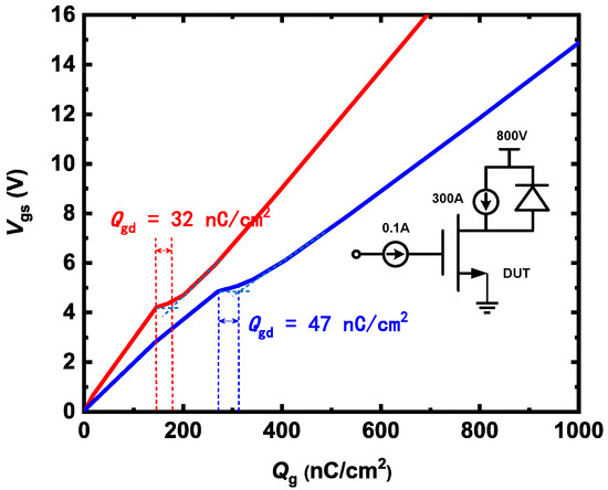
Figure 10. The gate charge characteristics of HJD-ATMOS and C-ATMOS.
Figure 11 shows the electric field distribution at the breakdown of HJD-ATMOS and C-ATMOS. The electric field at the gate oxide of HJD-ATMOS is smaller than that of C-ATMOS. This is because the presence of the Nch introduces a portion of the electric field into this region, which alleviates the electric field that the gate oxide withstands.
Although increasing the electric field at the heterojunction raises leakage current risk, it is a trade-off for improved reverse conduction performance. Figure 12 shows the blocking characteristics of the HJD-ATMOS and the C-ATMOS at room temperature and high temperature. At room temperature, the data are represented by solid lines, whereas at elevated temperatures, they are depicted by dashed lines. HJD-ATMOS and C-ATMOS have similar breakdown voltages at room temperature. But the leakage current of the HJD-ATMOS increases at high temperature due to the increased thermal energy of the charge carriers.
The generation of leakage currents, as demonstrated and discussed in Figure 6 and Figure 8, arises due to leakage occurring at the heterojunction, where higher Nnch and greater values of thickness h both contribute to this effect. By improving the semiconductor material growth process, reducing defects and traps, and enhancing the material quality and interface integrity, it is possible to mitigate non-ideal scattering and trap effects experienced by charge carriers at the heterojunction interface, thus suppressing the leakage current.
While the HJD-ATMOS structure does indeed experience leakage under temperature influence, this leakage is within acceptable limits, with the level of leakage current being 1 × 10⁻⁵ μA/cm2.
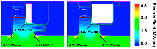
Figure 11. Electric field distribution for the HJD-ATMOS and the C-ATMOS at BV.
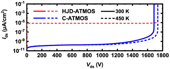
Figure 12. Blocking characteristics of the HJD-ATMOS and the C-ATMOS.
Figure 13 shows a double pulse test circuit for investigating switching characteristics. This is a common circuit configuration employed in device testing. Stray inductance is 10 nH, and load inductance is 80 μH. The gate voltage source (Vg) is turned on from −5 V to 15 V at t = 16 µs and turned off from 15 V to 0 V at t = 11 µs.
Figure 14 shows the switching waveforms of devices. The switching speed of the HJD-ATMOS is faster than that of the C-ATMOS with an external SBD diode, which results in a smaller switching loss. Figure 15 compares the switching losses between the two devices. In HJD-ATMOS, the turn-on loss (Eon) is 0.26 mJ/cm2, and the turn-off loss (Eoff) is 0.41 mJ/cm2, which demonstrate a reduction of 62.32% and 4.65%, respectively, compared to C-ATMOS.
The total switch loss of HJD-ATMOS is reduced by 40.29% compared to C-ATMOS. This is due to the smaller Qgd compared with the C-ATMOS. Reduced switching losses in power electronic devices are instrumental in improving operational longevity and reliability. As losses during switching are directly proportional to heat generation, a significant decrease in these losses curtails thermal build-up, mitigating the risk of device overheating and extending its operational life.
This reduction also sustains lower junction temperatures, crucial for preventing material degradation in high-power-density applications where maintaining low operating temperatures is vital for ensuring long-term stability and reliability. Furthermore, minimizing switching losses allows power converters and similar equipment to function efficiently at elevated frequencies without sacrificing efficiency, empowering designers to develop compact, lightweight systems while consistently meeting reliability standards.
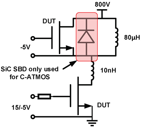
Figure 13. A circuit for simulating switching with a double pulsed test.
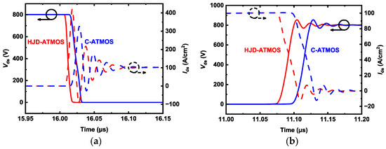
Figure 14. The switching characteristics of HJD-ATMOS and C-ATMOS, including the (a) turn-on process and (b) turn-off process.
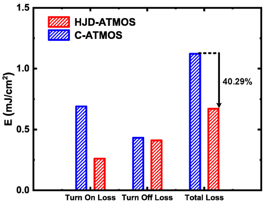
Figure 15. Switching loss comparison of IJ-ATMOS and C-ATMOS.
The majority of the process steps for HJD-ATMOS, including epitaxial growth, N+ source and P-well implantation, trench etching, P-base implantation, isolation oxidation, gate oxidation, polysilicon gate deposition, and metallization, are fully compatible with the manufacturing processes of C-ATMOS.
The N-channel region is formed by ion implantation at the bottom of the trench after trench etching. The split gate is formed by etching after trench oxidation, resulting in a thin layer of oxide between the gate and the P-Poly-Si. The gate-P-Poly-Si trench isolation layer is formed by thermal oxidation, and the trench oxide layer is fully etched and filled with P-Poly-Si.
Table 2 compares the HJD-ATMOS and the C-ATMOS in terms of their main characteristics. Dynamic FOM indicates the value of Ron,sp × Qgd. The HJD-ATMOS performs better due to the integrated HJD structure.
Table 2. Device characteristics comparison.
4. Conclusions
This paper proposes a novel asymmetric trench SiC MOSFET with a heterojunction diode. The performance of HJD-ATMOS and C-ATMOS is compared in detail. It can be observed that HJD-ATMOS demonstrates superior third-quadrant performance with a lower Vcut-in because of the integrated HJD. Compared with C-ATMOS, the Qgd of HJD-ATMOS has decreased by 31.91%. This is because the split gate design further reduces the total gate charge, which reduces the switching loss of the HJD-ATMOS device without affecting other key characteristics.
As a result, HJD-ATMOS eliminates bipolar degradation and reduces the turn-on loss from 0.69 mJ/cm2 in C-ATMOS to 0.26 mJ/cm2. With its advantageous features, HJD-ATMOS is a strong contender for power electronic applications.
Authors
Yiren Yu, Zijun Cheng, Yi Hu, Ruiyi Lv, Shengdong Hu.
Original – MDPI
-

Ideal Power Inc. announced that it has priced its previously announced underwritten public offering of 2,000,000 shares of its common stock (or pre-funded warrants in lieu thereof) at an offering price of $7.50 per share of common stock. Ideal Power has granted the underwriter a 30-day option to purchase up to 300,000 additional shares of its common stock on the same terms and conditions. The Company expects to close the offering on March 28, 2024, subject to customary conditions.
Titan Partners Group, a division of American Capital Partners, is acting as sole book-running manager for the offering.
The gross proceeds to the Company from the offering are expected to be approximately $15 million, before deducting underwriting discounts, commissions and other estimated offering expenses payable by the Company. The Company intends to use the net proceeds from this offering for general corporate and working capital purposes.
The offering is being made pursuant to an effective “shelf” registration statement on Form S-3 (File No. 333-269060) previously filed with the Securities and Exchange Commission (the “SEC”) on December 29, 2022, and declared effective by the SEC on January 9, 2023.
The securities may be offered only by means of a prospectus and prospectus supplement that form a part of the registration statement. A preliminary prospectus supplement and the accompanying prospectus relating to and describing the terms of the offering have been filed with the SEC. The final terms of the offering will be disclosed in a final prospectus supplement to be filed with the SEC.
Electronic copies of the final prospectus supplement and the accompanying prospectus relating to the offering, when available, may be obtained by visiting the SEC’s website at www.sec.gov or by contacting Titan Partners Group, LLC, a division of American Capital Partners, LLC, 4 World Trade Center, 29th Floor, New York, New York 10007, by phone at (929) 833-1246 or by email at prospectus@titanpartnersgrp.com.
Original – Ideal Power
-

Decarbonization and digitalization are the two central challenges of our time, but they rely on new and advanced technologies. At embedded world 2024 in Nuremberg, Infineon Technologies AG will demonstrate how its innovative semiconductor solutions support and drive these advancements.
Microcontrollers in particular play an important role as they are at the heart of a wide range of applications, from electric vehicles and renewable energy systems to smart homes and industrial automation. For this reason, Infineon showcases high-quality microcontrollers designed with the latest technologies and innovative features such as enhanced security and high accuracy, offering excellent performance with low power consumption.
Under the motto “Driving decarbonization and digitalization. Together.” Infineon invites its customers to embedded world 2024 to demonstrate innovative semiconductor solutions that contribute to a more sustainable future. In addition, customers can register for Infineon’s digital platform – the perfect place to dive deeper into the various technologies presented at EW during and after the event. The Infineon booth in Hall 4A (booth #138) will present highlights from the consumer and IoT, automotive, and industrial sectors.
Consumer and IoT: With its broad portfolio of IoT solutions, Infineon supports manufacturers in providing consumers with more comfortable, secure, and energy-efficient homes and buildings by utilizing the company’s latest microcontroller, sensor, security, and connectivity solutions. In this area, visitors will discover:
- Robotics development platform: The platform includes hardware and software solutions for key robotics subsystems such as main and motor controllers, battery management systems and sensors, which enable developers to get robots up and running faster and easier.
- Better sleep quality with XENSIV™: Leveraging Infineon’s 60 GHz radar, PSoC™ and Wi-Fi® technologies, the XENSIV Sleep Quality Service is designed to measure and optimize the user’s sleep based on their individual needs.
- Simplifying air quality monitoring and optimizing energy efficiency with the new XENSIV PAS CO2 5V kits: The XENSIV PAS CO2 5V Sensor2Go kit provides developers with seamless CO 2 sensor integration and a plug-and-play solution. The effortless connection to the graphical user interface (GUI) allows users to accurately analyze CO 2 data in real time from multiple kits.
- Land a rocket on the Edge: This fun game demonstrates the PSoC Edge device’s ability to integrate multiple functions such as high-performance computing, graphics processing and display, acoustic activity recognition, speech recognition, sensing and gesture recognition with ML in the same chip and application.
Automotive: As a leading supplier of automotive solutions, Infineon focuses on making smart cars a reality with proven microcontroller, connectivity, security, and sensor technologies for the industry. The company’s microelectronics play a critical role in delivering zero-emission vehicles that are smart, connected, safe and reliable.
- AI-based siren recognition: Infineon showcases an autonomous car that recognizes emergency vehicles by their characteristic siren sound and reacts accordingly without violating traffic regulations. This system solution combines MEMS microphones, a microcontroller unit (MCU), and AI software from Imagimob.
- Next generation eMobility: Infineon enables next-generation vehicles with the AURIX™ TC4x microcontroller family and the AURIX Development Studio (ADS). With these solutions, manufacturers can easily implement modern ADAS, advanced automotive E/E architectures and affordable Artificial Intelligence (AI) applications.
- TRAVEO™ T2G Cluster 6M Lite Kit: With the TRAVEO T2G CYT4DL device prototypes can be implemented in the shortest possible time and at minimal cost.
Industrial: Infineon supports smart factories and provides manufacturers with a broad sensor portfolio and an extensive partner network. In this way, the company enables reliable data acquisition and processing that enables condition monitoring and predictive maintenance in various Industry 4.0 use cases:
- Predictive maintenance: In this sector, Infineon will present a portable HVAC system equipped with the XENSIV Predictive Maintenance Evaluation Kit. The demo includes a TinyML model and a cloud-based AI service solution generator.
At the Infineon booth, the company has set up a comprehensive series of TechTalks. The seven presentations will cover a wide range of different topics, from software to products, and from consumers to industry. Full details of all Infineon conference presentations, technical workshops and TechTalks can be found here.
Daily program of the Tech Talks
- “Ambient sensing: Infineon radar solutions: How Infineon’s tools and enablement can accelerate your time to market” at 10:00 a.m. presented by Firas Labidi
- “Embedded AI and safety – Embedded AI will enable the innovations for next generation of electric vehicle and autonomous driving” at 11:00 a.m. presented by Jürgen Schäfer
- “Accelerate your product development with system reference designs” at 12:00 p.m. presented by Jaya Bindra
- “Addressing the next generation of Edge AI devices with PSoC Edge” at 1:00 p.m. presented by Rebecca Phillips
- “TRAVEO T2G MCUs for automotive HD front lighting” at 2:00 p.m. presented by Maniacherry Devassy Anu
- “Unlocking the power of Edge AI with Imagimob and ModusToolbox™” at 3:00 p.m. presented by Alexander Samuelsson
- “Infineon’s solutions for robotics” at 4:00 p.m. presented by Nenad Belancic
Original – Infineon Technologies
-

The Specialty Thin Film (STF) division of Vishay Intertechnology, Inc. announced that its Electro-Films (EFI) factory in Warwick, Rhode Island, has been certified to the IATF 16949:2016 quality standard for the IGBR family of back contact wirebondable gate resistors, designed to reduce noise in silicon carbide (SiC) MOSFET power modules.
Based on ISO 9001:2015 — with additional automotive customer-specific requirements — IATF 16949:2016 is the global technical specification and quality management standard for the automotive industry. With this certification, the quality management system at the EFI Warwick factory is now certified to ISO 9001:2015 for all products, and IATF 16949:2016 for IGBR resistors. In addition, its environmental management system is certified to ISO 14001:2015 and ISO 45001:2018.
Original – Vishay Intertechnology
-

In the paper “Milliseconds Power Cycling (PCmsec) Driving Bipolar Degradation in Silicon Carbide Power Devices”, Sibasish Laha from Fraunhofer IISB and his co-authors Jürgen Leib, Andreas Schletz, Martin Maerz, Christian Liguda, Firas Faisal and Davood Momeni describe an innovative approach to silicon carbide (SiC) power cycling.
Until now, bipolar degradation (BD) tests have not been sufficiently differentiated in the investigation of failure and fault mechanisms for SiC power devices. SiC power products may experience voltage degradation which stems from the stacking faults (SFs) growth, commonly known as BD. To properly evaluate the BD impact on the electric performance of devices, it is important to distinguish it from other stress-related degradation such as power metal or interconnection.
This aspect has not yet been addressed, although the BD mechanism is well understood. The paper outlines a methodology by modifying the power cycling test (PCsec) to PCmsec in order to systematically investigate the effect of BD while controlling the impact of thermal degradation. This method enables a thorough evaluation of the distinct influences of both degradation contributors.
The complete paper will soon be available in the CIPS proceedings. Until then, feel free to download the paper presentation on event page.
There you can also find all our contributions to CIPS 2024:- Modified Approach for the Rainflow Counting Analysis of Temperature Load Signals in Power Electronics Modules – Oral presentation by S. Letz; Co-authors: D. Zhao, J. Leib, B. Eckardt, M. März
- Milliseconds Power Cycling (PCmsec) Driving Bipolar Degradation in Silicon Carbide Power Devices – Oral presentation by S. Laha; Co-authors: D. Momeni, J. Leib, A. Schletz, M. März, C. Liguda, F. Faisal
- Challenges of Junction Temperature Calibration of SiC MOSFETs for Power Cycling – a Dynamic Approach – Poster by J. Breuer, F. Dresel, A. Schletz, J. Klier, J. Leib, M. März, B. Eckardt
- Wide Bandwidth PCB Rogowski Coil Current Sensor with Droop Suppression and DC Restoration for In-Situ Inverter Measurements – Poster by S. Quergfelder, J. Sax, T. Heckel, B. Eckardt, M. März
Original – Fraunhofer IISB
