-

Aehr Test Systems announced preliminary financial results for its third quarter of fiscal 2024 ended February 29, 2024. Preliminary results reflect delays in wafer level burn-in system orders for semiconductor devices used in electric vehicles that have created a short-term gap in revenue and profitability. Additionally, Aehr provided updated revenue guidance for its full fiscal year ending May 31, 2024.
For the fiscal third quarter ended February 29, 2024, Aehr expects:
- Revenue of approximately $7.6 million
- GAAP net loss of approximately $1.5 million to $1.8 million, or $0.05 to $0.06 per diluted share
- Non-GAAP net loss of approximately $0.9 million to $1.2 million, or $0.03 to $0.04 per diluted share, which excludes the impact of stock-based compensation
- Bookings of $24.5 million
- Backlog as of February 29, 2024, of $20 million
For the fiscal 2024 full year ending May 31, 2024, Aehr expects:
- Total revenue of at least $65 million
- GAAP net income of approximately $11 million or more, or $0.38 per diluted share
- Non-GAAP net income of approximately $14 million or more, or $0.48 per diluted share, which excludes the impact of stock-based compensation
An explanation of the use of non-GAAP financial measures and a reconciliation of Aehr’s non-GAAP financial measures to the most directly comparable GAAP financial measures will be included when Aehr releases its full financial results for the fiscal 2024 third quarter on April 9, 2024.
Aehr Test Systems President and CEO Gayn Erickson commented: “As we discussed in our second quarter earnings call, we had seen several push outs of forecasted orders by current and new customers that impacted our fiscal year revenue. We believe that this was due to two key factors. There is clearly softness in the overall semiconductor capital spending, particularly in automotive applications, related to a glut in inventory driving down near-term orders to these companies and has caused them to push out capital spending and drive cost reductions. Multiple companies including the companies we had expected orders from have publicly discussed inventory related headwinds in their public earnings calls and press releases. In addition, we have seen specific shifts in order timing of our equipment used for wafer level test and burn-in of silicon carbide power semiconductors used in electric vehicles. In just the last two weeks of the quarter, we saw delays in orders for silicon carbide systems with customer-requested ship dates within the quarter as well as a last-minute push out by a customer of a system in our backlog. The net effect of this was a significant shift in revenues out of the third and fourth quarters. Until this time, we had been hearing from those customers that their silicon carbide-based capital investments were not being impacted.
“It is now clear that the recent overall softness in semiconductors and the impact of shifts in electric vehicle introductions and ramps are impacting our bookings and revenue forecasts more than we understood only two months ago at our last earnings call. We now expect this to last for another quarter or two before the orders resume based on the latest roll up of direct forecasts from over a dozen silicon carbide companies. We are now forecasting revenue for the full fiscal year to be $65 million or more, representing revenue of at least $15.4 million in our fiscal fourth quarter. We still expect to finish the year with near or above record annual revenue for the year.
“Our discussions with customers indicate to us that the key markets Aehr is addressing for semiconductor wafer level test and burn-in have significant long-term growth opportunities that will continue to expand throughout this decade. Despite what we believe are temporary delays in current and new customer orders, we believe Aehr will experience significant order, revenue, and earnings growth from these market opportunities. Our unique, proprietary wafer level test and burn-in offering for semiconductors addresses the need for the critical reliability testing and screening of semiconductors used in the worldwide electrification infrastructure, battery and hybrid electric vehicles, data and telecommunications and data storage, machine learning and Artificial Intelligence processors and communications chips, and in the large and growing semiconductor memory market. We look forward to discussing the impact and timing of these markets and the increase in customer engagements in all these markets on our earnings call planned for April 9th.”
The foregoing preliminary financial information reflects management’s current views with respect to the Company’s financial results. These preliminary results remain subject to the completion of normal quarter-end accounting procedures and closing adjustments. Aehr plans to release its full financial results for the fiscal 2024 third quarter on April 9, 2024, and will provide the time and conference call details in a later press release. No independent registered public accounting firm has reviewed, examined, or performed any procedures with respect to, nor have they expressed any form of assurance on, these preliminary estimated results.
Original – Aehr Test Systems
-

Siltronic AG plans to gradually cease production of polished and epitaxial small diameter wafers at its Burghausen site. The process, which excludes unpolished wafers, is set to be completed in the course of 2025.
Siltronic currently produces wafers with a diameter of 300 mm, 200 mm and wafers with smaller diameters (SD) of up to 150 mm. The SD wafer technology was developed primarily in the 1990s and earlier. The most significant technological breakthroughs in recent decades have been achieved with larger diameters, which also show the highest growth potential. An average volume growth of 6 percent per year is expected for 300 mm wafers.
“SD wafer production at Siltronic originated in Burghausen in 1968. It has contributed to our success for many years, thanks to the outstanding work of our employees. However, the wafer industry has evolved significantly due to structural changes and innovations. Demand has increasingly shifted to wafers with larger diameters and improved properties, while SD wafers are approaching the end of their life cycle. This has led to a notable decline in volumes, which recently had a negative impact on earnings. As this will likely continue to intensify in the coming years, we have decided, together with the Supervisory Board, to gradually reduce the production of small diameters and to cease it in the course of 2025,” comments Dr. Michael Heckmeier, CEO of Siltronic AG.
“Despite this decision the Burghausen site remains of crucial importance for Siltronic. Our global technology as well as research and development center, the production of 300 mm wafers and 200 mm hyperpure silicon ingots as well as a large part of our administrative functions are located here,” Michael Heckmeier continues.
Just 25 years ago, more than half of the silicon wafer market consisted of wafers with a diameter of up to 150 mm. Today, it is less than five percent, based on data published by the industry organization SEMI. This is the result of customers reducing or ceasing their production of small wafers due to the dynamic technological developments in the semiconductor industry. In addition, competition, particularly from China, is now clearly felt in the small diameters.
In the past financial year, SD wafers accounted for a single-digit percentage of the Group’s sales. The impact on earnings has already been clearly negative in recent months. Approximately 400 people are employed in the small diameters, about half of whom are on fixed-term and temporary contracts. The aim is to reduce the core workforce in a socially responsible manner through demographic change and partial retirement, and to avoid layoffs for operational reasons.
“Due to structural changes in the market, we assume that SD wafers will not recover and that their impact on earnings would be considerably negative in the coming years. We have therefore decided to take this difficult but necessary step. At the same time, our goal is to ensure that workforce reductions at Siltronic are socially responsible and no layoffs are made for operational reasons. After the end of the SD wafer production and the subsequent dismantling measures that may be necessary, our EBITDA margin will improve by around one to two percentage points in the medium term,” adds Claudia Schmitt, CFO of Siltronic AG.
Original – Siltronic
-

GlobalWafers has been responding to the challenges of global climate risks by dedicating to environmental sustainability in its manufacturing processes, renewable energy adoption and business strategies.
GlobalWafers took the initiative in 2021 and committed to 100% renewable energy usage by 2050 in its global operations, and formally joined RE100 initiative in 2022 to reaffirm its determination to sustainable operation. As one of the very few semiconductor manufacturers that owns its solar power plants, GlobalWafers actively invests solar power plants to gain more flexibility and advantages in energy use, such as reducing carbon emissions, enhancing operational resilience, and meeting regulatory requirements more effectively. While the demand for clean energy continues to grow, GlobalWafers looks forward to positioning itself for long-term success in a rapidly evolving market.
GlobalWafers’ commitment to green wafer manufacturing is exemplified by its operation sites in Denmark and Italy. GlobalWafers’ Danish site, Topsil, is poised to become the first semiconductor crystal manufacturing site to utilize its own installed 100% green electricity during 2H of 2024.
By constructing a new solar park with an estimated capacity of 10.2MW, the power plant is expected to generate 9,500,000 kWh per year. Accordingly, Topsil is set to produce more electricity than it consumes, marking a significant milestone in GlobalWafers’ green manufacturing process.
Besides, GlobalWafers’ Italian site, MEMC Electronic Materials S.p.A., is also expected to reach 100% green electricity usage in the 12” new line during the capacity ramp-up stage in 2025. Leveraging power purchase agreements, installation of solar panels, and actively exploring alternative clean energy sources, the Italian site demonstrates GlobalWafers’ multifaceted approach to achieving its RE100 target.
With its global presence, GlobalWafers emphasizes local supply to minimize transportation distances, consequently reducing the carbon footprint and the potential impact of carbon tariffs, while also mitigating geopolitical risks. In a proactive move, GlobalWafers has implemented Internal Carbon Pricing mechanism, urging each site to consider the environmental impact of its operations. By accounting for the true cost of carbon emissions, GlobalWafers aims to foster a culture of informed decision-making that prioritizes sustainability.
To showcase solidarity with global transition towards net zero emission, GlobalWafers participates in the “Earth Hour 60” initiative again this year with affiliated group companies. On March 23rd at 8:30 pm, GlobalWafers’ Taiwan sites will switch off unnecessary lights and power-consuming equipment for one hour. This symbolic gesture underscores the GlobalWafers continuous commitment to energy conservation and carbon reduction.
As the world grapples with the challenges of climate change, GlobalWafers, as a long-term partner of its customers, not only actively considers implementing SBTi, but also remains steadfast in its pursuit of a sustainable environment. By embracing renewable energy, reducing carbon emissions, and strengthening green wafer manufacturing, GlobalWafers is leading the charge towards a greener, more sustainable future.
Original – GlobalWafers
-

Innoscience Technology firmly denounces the accusations made by Infineon Technologies Austria AG in a recent patent infringement lawsuit against three Innoscience entities. Infineon filed this lawsuit in a U.S. district court in California on March 13, 2024, and asserted a single U.S. patent.
Innoscience denies Infineon’s allegations of patent infringement as well as the validity of the Infineon patent. Innoscience will vigorously defend itself and is confident that it will prevail. Infineon’s intention with this litigation is also in question, as it has asserted a patent that has significant defects. Particularly, even a cursory review of Infineon’s patent portfolio reveals that the alleged “invention” of the asserted patent was already disclosed in Infineon’s own earlier prior art patents, raising concerns that it may have committed fraud on the United States Patent and Trademark Office, for not making proper disclosures during the prosecution of the asserted defective patent.
In addition, contrary to Infineon’s wrong characterization that the claims of the asserted defective patent “cover core aspects of GaN power semiconductors,” the lawsuit only concerns a small fraction of Innoscience’s packaged high-voltage (650V-700V) GaN transistors and does not affect the vast majority of its other products (including unpackaged transistors and wafers, low-voltage transistors, and certain packaged transistors).
Therefore, the lawsuit should have little to no effect on Innoscience’s current ability to make, use, sell, offer to sell, or import into the United States its products for customers. Innoscience respects others’ valid IP rights and is also dedicated to developing its own IP portfolio. Despite being an eight-year old company, Innoscience has filed more than 800 patent applications globally. Innoscience’s R&D team boasts 500+ technical experts across the world.
Through continuing innovation, Innoscience has produced GaN devices to power a diverse range of products, from power delivery chargers to data centers and smartphones, showcasing its ability to align with evolving application demands and adapt to diverse customer specifications.
Moreover, Innoscience has always sought a cooperative and mutually beneficial approach to develop the global GaN industry, even among others in the same industry. Innoscience intends to prevail in this pending lawsuit and is determined to remain a trusted and reliable partner for its customers and contribute to their success by offering top-notch and versatile products and solutions based on Innoscience’s home-grown, superior technologies.
Original – Innoscience Technology
-
Abstract
In this study, a novel integrated 4H-SiC reverse-conducting gate turn-off thyristor (GTO) featuring an N-type floating (NF) structure is proposed. The proposed NF-structured 4H-SiC GTO outperforms conventional reverse-conducting GTOs in forward conduction, effectively eliminating the snapback phenomenon.
This is achieved by increasing lateral resistance above the P-injector and modifying the electron current path during early turn-on. NF structures with a doping concentration of 2 × 1014 cm−3 and thicknesses exceeding 4 μm have been indicated to successfully eliminate the snapback phenomenon. Moreover, the anode-shorted structure enhances the GTO’s breakdown voltage and concurrently reduces turn-off losses by 85% at low current densities.
1. Introduction
In recent years, advancements in power distribution and energy transmission applications, including smart grids, ultra-high voltage power transportation, and pulse power technology, have heightened the demand for high-voltage power devices. Typically, conventional silicon (Si) power devices can withstand voltages up to 8 kV. Beyond this limit, complex arrangements of converters or devices become necessary, especially in ultra-high voltage contexts.
This necessity has shifted the focus towards wide bandgap (WBG) semiconductors, particularly 4H-SiC, renowned for their superior material characteristics. 4H-SiC is increasingly favored for fabricating ultra-high voltage and high-frequency power devices because of its exceptional properties: a bandgap three times wider than that of silicon, a critical breakdown electrical field ten times higher, and an electron saturation velocity surpassing silicon by an order of magnitude.
In recent years, significant strides have been made in refining the SiC epitaxial growth process, marked by noteworthy advancements in enhancing charge carrier lifetimes and reducing bulk- and interface-trap densities. These improvements have been instrumental in achieving substantial progress in the development of high-voltage SiC devices.
Wolfspeed (formerly known as Cree Inc., Durham, NC, USA) have announced their development of SiC MOSFETs with impressive blocking voltages of 10 kV and 15 kV. Concurrently, there has been a technological breakthrough in bipolar devices rated above 20 kV, achieving PIN diodes with blocking voltages ranging from 7 to 39 kV, further pushing the boundaries in high-voltage device engineering. In addition, 10 kV SBD and JBS diodes have also been produced.
In 2015, the voltage and current capabilities of SiC IGBTs saw a significant enhancement, reaching 27.5 kV/20 A. In 2013, Cree Inc. advanced the SiC p-GTO’s performance to 20 kV, followed by the development of a 15 kV SiC n-GTO in 2019. Furthermore, in 2017, a SiC Emitter Turn-Off Thyristor (ETO) p-ETO with a blocking voltage of 22 kV was reported, exemplifying continued advancements in SiC device technology.
Additionally, researchers are focusing on the stacking technology of SiC-based power devices for ultra-high voltage applications. In the study ‘Theoretical and Experimental Study of 22 kV SiC Emitter Turn-OFF (ETO) Thyristor’, an assessment of the forward current handling capacities of 15 kV SiC GTO (p-type), IGBT, and MOSFET at temperatures of 25 °C and 125 °C was conducted.
This analysis clearly indicates that the SiC GTO outperforms in terms of managing higher currents with the least forward voltage drop, marking it a key player for the next generation of ultra-high power devices. In the research documented in ‘Evaluation of Ultrahigh-Voltage 4H-SiC Gate Turn-OFF Thyristors and Insulated-Gate Bipolar Transistors for High-Power Applications’, simulation models were employed to validate that within a range of 20–50 kV, SiC GTOs exhibit a voltage drop of 3.4–7.8 V at a current density of 20 A/cm2 at room temperature, whereas IGBTs display a voltage drop between 4.2 and 10 V under similar conditions.
The underlying reason for this enhanced performance of SiC GTO, from the viewpoint of semiconductor current conduction, is its capability for bidirectional carrier injection and pronounced conductivity modulation in the drift region. Therefore, the SiC GTO is emerging as a highly viable option for ultra-high voltage power applications.
However, the intense conductivity modulation effect leads to an increased turn-off time, subsequently slowing down the switching speed. In the case of GTO devices, turn-off losses constitute a major part of the overall switching losses, prompting considerable efforts in recent years to minimize these losses. To enhance GTO performance, various structures such as Integrated Gate-Commuted Thyristors (IGCT), Emitter Turn-Off (ETO) Thyristors, and Reverse-Conducting GTOs (RC-GTO) have been proposed.
The Reverse-Conducting GTO (RC-GTO) introduces an innovative design that combines a diode with a GTO at the cellular level. This integrated architecture functions as a high-voltage forward switch and, when reversed, operates as a continuous current diode. Traditional GTOs, lacking reverse conduction capability, necessitate parallel connection with a reverse diode.
Thus, compared to conventional GTOs, RC-GTOs offer enhanced power density, streamlined system design, and improved thermal cycling of the chip. However, like RC-IGBTs, conventional RC-GTOs suffer from an undesirable snapback effect, which hinders the device from fully turning on. In this study, a novel integrated SiC Reverse-Conducting GTO (RC-GTO) structure featuring an N-type floating region (NF-RC-GTO) is presented. This design effectively suppresses and eliminates the snapback phenomenon, minimally impacting the primary performance. Additionally, it features low turn-off loss at low current densities.
2. Device Structure and Mechanism
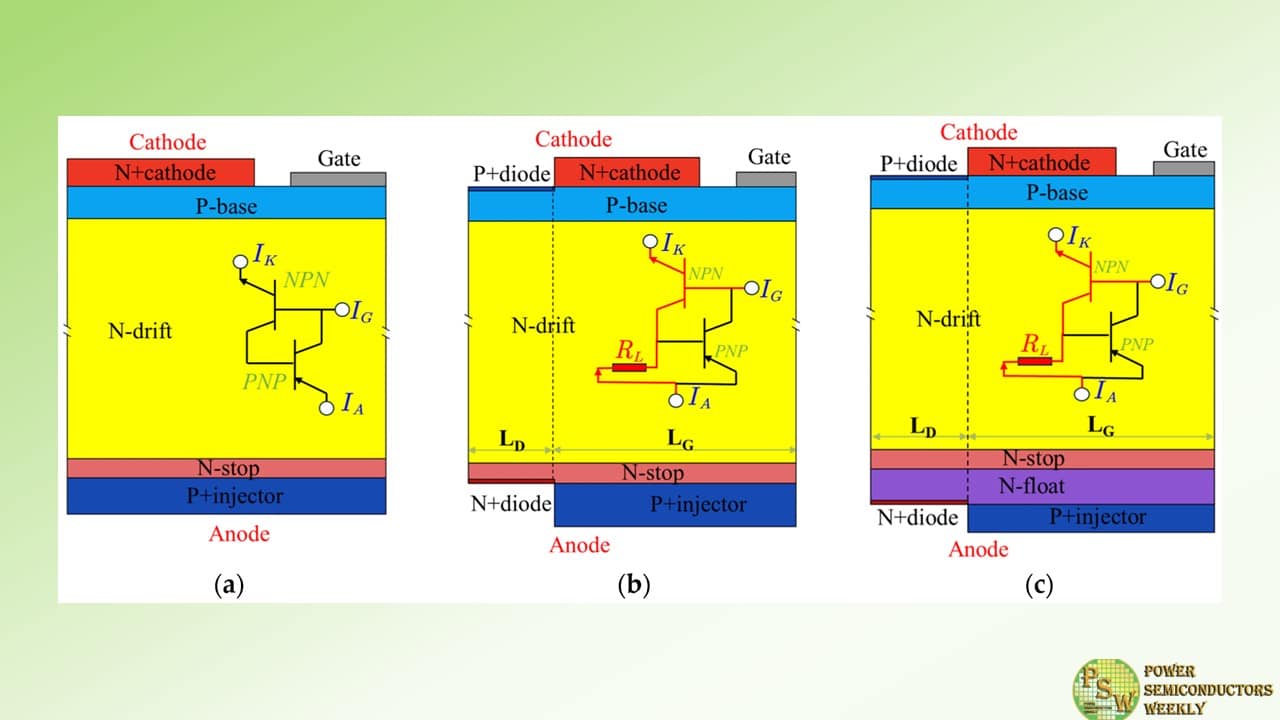
Figure 1a–c illustrate the simulation structures and equivalent circuit diagrams of the GTO, conventional RC-GTO (con-RC-GTO), and NF-RC-GTO, respectively. The SiC GTO is comprised of five layers: p-n-n-p-n, which functionally resemble two back-to-back PNP and NPN bipolar junction transistors (BJTs). The currents in these two BJTs are interdependent, and the device activates when the sum of the common-base current gains, denoted as αPNP and αPNP for the PNP and NPN BJTs, respectively, exceeds 1.
Compared to a standard GTO, both the conventional RC-GTO (con-RC-GTO) and the NF-RC-GTO feature an anode-shortened structure and a cathode-shortened structure, functioning as a reverse diode. In the equivalent circuit of a SiC RC-GTO, the additional connection to the N-drift region is modeled as a resistor (RL) placed parallel between the base and emitter terminals of the inherent PNP bipolar transistor (BJT). RL is nonlinear, primarily determined by the shape and doping concentration of the N-stop (and for NF-RC-GTO, also the N-float) regions.
During the initial phase of forward-conduction mode, the RC-GTO operates akin to an NPN BJT. This continues until the conduction current is sufficient to cause the voltage drop across RL to exceed 2.7 V, which is approximately the turn-on threshold voltage of a conventionally doped SiC PN junction at room temperature, fully activating the emitter-base junction of the inherent PNP transistor.
Once activated, the inherent PNP transistor contributes to conductivity modulation in the N-drift region, leading to a significant decrease in the resistance between the cathode and anode of the device. Subsequently, the RC-GTO transitions to operate as a conventional GTO. This shift from NPN BJT to GTO operation is marked by a voltage jump and an exponential increase in anode current, a process known as the snapback phenomenon.
Figure 1. Structures and equivalent circuit diagrams of the devices under study. (a) GTO; (b) conventional RC-GTO; (c) NF-RC-GTO.
To mitigate the snapback effect, the NF-RC-GTO incorporates an additional N-float layer with a lower doping concentration (such as 2 × 1014 cm−3). This layer boosts the lateral resistance above the P-injector, directing current flow through areas of higher resistance and enabling the emitter-base junction of the intrinsic PNP bipolar transistor to activate at much lower currents.
It is important to note the symmetrical relation of the cathode-shortened region to the gate structure in the NF-RC-GTO, which simplifies the formation of the cathode-shortened structure, especially when compared to traditional SiC-nGTO fabrication processes.
The performance of the various structures was simulated using Synopsys Sentaurus Technology Computer-Aided Design software, which computes fundamental physical partial differential equations and physical models, such as the Poisson equation and diffusion and transport equations, to facilitate the simulation of the structure and electrical characteristics of semiconductor devices.
Please note, all subsequent results are derived from simulation experiments. The basic physical models utilized in the TCAD simulations encompass impact ionization, incomplete ionization, Shockley–Read–Hall and Auger recombination, doping concentration-dependent carrier lifetime, and electric field and doping concentration-dependent carrier mobility.
The average lifetimes of carriers are defined as 2.5 µs for electrons and 0.5 µs for holes, which align with values commonly found in commercially available epitaxial layer structures. The standard parameters for the 13 kV SiC NF-RC-GTO, SiC con-RC-GTO, and con-GTO are compiled and presented in Table 1.
Table 1. Device parameters for simulations.
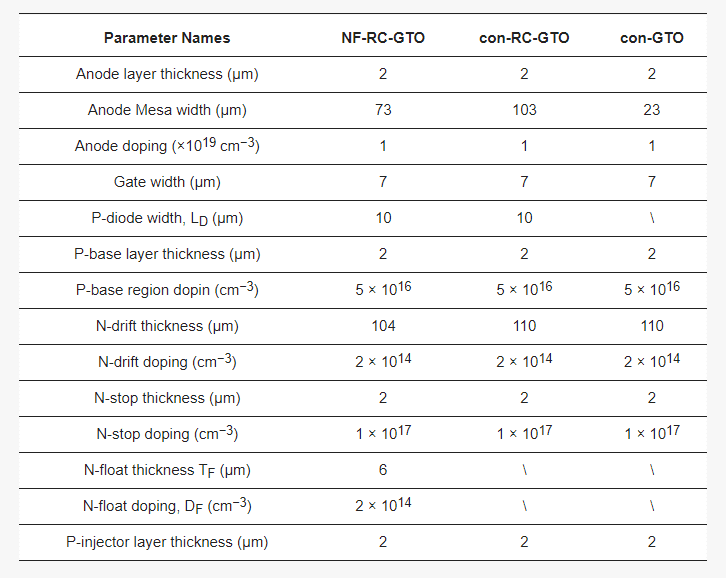
Figure 2 displays the current–voltage (I–V) characteristics for the GTO, con-RC-GTO, and NF-RC-GTO. In terms of forward turn-on performance, the conventional GTO exhibits optimal characteristics with a smooth transition, notably absent of any snapback effect.
For the RC-GTO variants, prior to the turn-on of the anode P/N diode, the devices exhibit behavior akin to an NPN BJT, a result of the additional electron excess provided by the N+ diode region. Specifically, in the case of the con-RC-GTO, a broader LG dimension diminishes the snapback effect. As LG widens from 110 μm to 120 μm, there is a notable reduction in the snapback voltage from 6.11 V down to 4.83 V.
Conversely, the NF-RC-GTO sees the complete elimination of the snapback effect with a reduced LG width of just 80 μm, affirming the effectiveness of the N-float structure in mitigating this issue. Furthermore, the forward conduction voltage drop (measured at a current density of 100 A/cm2) is comparable to that of the con-RC-GTO.
It is important to consider that an oversized LG dimension may lead to an uneven distribution of current within the device. This imbalance can result in thermal concentration issues, and additionally, it has the potential to diminish the available space for the reverse PN diode structure.
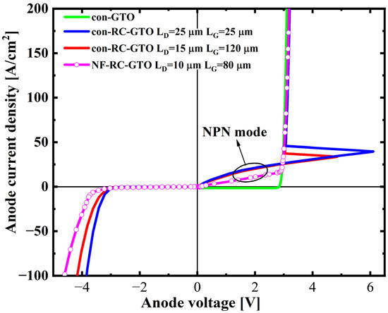
Figure 2. The current–voltage (I–V) characteristics of the GTO, con-RC-GTO, and NF-RC-GTO.
Figure 3 illustrates the initial paths of electron and hole currents during the conduction mode. Specifically, Figure 3a depicts the flow of electron current into the P-collector, bypassing the N-stop layer and entering the N-float layer in the NF-RC-IGBT under unipolar mode. This dual-layer structure effectively channels the current flow through the N-float region, significantly increasing the path resistance.
The current flow lines shown in Figure 3b confirm this. The voltage across the P-injector and N-float junction, distant from the N region, reaches at least 2.7 V at the earliest stage. Subsequently, the P-injector at this juncture begins to inject holes, facilitating conductivity modulation. Consequently, the device transitions into operating as a GTO.
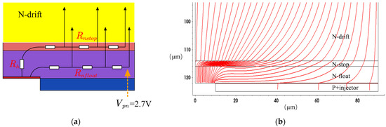
Figure 3. (a) Current flow path; (b) current flow lines at the Anode side of the NF-RC-GTO in low current density mode.
The simple snapback model used for Figure 3a can be described as follows:

For the NF-RC-GTO, the N-float layer is pivotal in directing the current flow through areas of high resistance. This underscores the necessity for meticulous design of both the doping concentration and the geometry of the N-float region to more effectively suppress the snapback phenomenon.
3. Results
Figure 4 displays the characteristic curves of the forward off-state breakdown voltage. The breakdown voltages for the NF-RC-GTO, con-RC-GTO, and con-GTO are 15,303 V, 15,992 V, and 13,730 V, respectively. Both the NF-RC-GTO and con-RC-GTO, featuring an anode-short structure, exhibit higher breakdown voltages compared to the conventional GTO. Notably, the NF-RC-GTO shows an 11.4% improvement over the con-GTO.
This enhanced performance is attributed to the anode-short circuit structure, which allows leakage current from the reverse-biased junction to directly exit through the short-circuited anode. This mechanism also prevents hole injection at the P+ injector region, reducing the common-base current gain of the anode PNP BJT, thereby increasing the forward breakdown voltage. The slightly lower breakdown voltage of the NF-RC-GTO, compared to the con-RC-GTO, is due to the NF structure, which results in a shorter ndrift structure (104 µm).
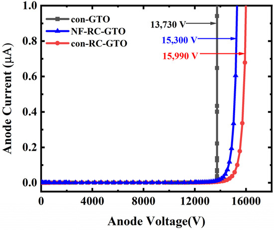
Figure 4. BV curves of the con-GTO, con-RC-GTO, and NF-RC-GTO, respectively. The gate voltage is zero.
Figure 5 provides insight into the effect of doping concentration in the float region on the forward and reverse performance of NF-RC-GTOs, which are characterized by a consistent thickness of 4 μm and an LG length of 80 μm. The figure reveals that as the doping concentration decreases, the snapback voltage also reduces, and the snapback phenomenon completely vanishes at a doping concentration of 2 × 1014 cm−3.
This trend can be attributed to the increased lateral resistance above the P-injector resulting from the lower doping concentration, consequently leading to a reduced snapback voltage. Additionally, during the initial turn-on phase, the current in the NPN mode diminishes as the lateral resistance increases. It is also observed that with a higher doping concentration, the current handling capability slightly decreases. This is due to an increase in the compound current within the NF region, which negatively affects the hole injection efficiency in the anode region.
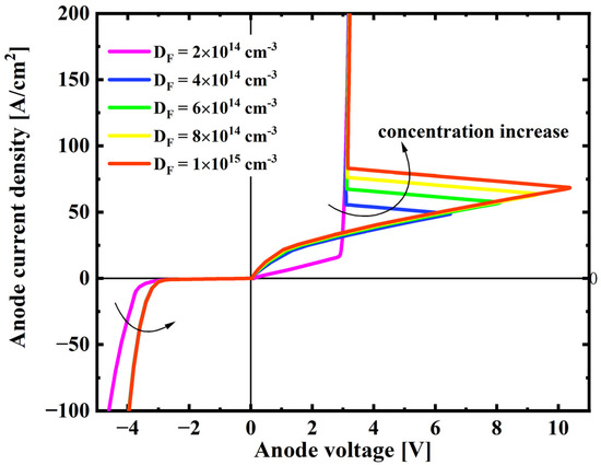
Figure 5. Forward and reverse conduction characteristics of the NF-RC-GTO with different N-float doping concentration (DF).
Figure 6 delineates the impact of the N-float structure’s thickness on the forward and reverse performance of NF-RC-GTOs. These devices share a consistent doping concentration and LG dimension for the N-float structure, at 2 × 1014 cm−3 and 80 μm, respectively.
The figure indicates that the snapback voltage decreases with an increase in the thickness of the N-float structure. Notably, the snapback phenomenon is eliminated when the thickness exceeds 3 μm. This effect can be attributed to the thicker N-float structure reducing the direct flow of NPN mode current through the N-stop region to the anode-short structure during the initial turn-on phase.
As a result, a higher proportion of electrons flow through the N-float region to the anode-short structure, facilitating earlier hole injection in the anode P-injector/N-float region. Furthermore, Figure 6 also reveals that variations in the thickness of the N-float structure within a certain range do not significantly affect the NF-RC-GTO’s forward and reverse high-current handling capability.
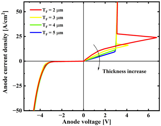
Figure 6. Forward and reverse conduction characteristics of the NF-RC-GTO with different thickness of N-float structure (TF).
The transient characteristics of the newly proposed NF-RC-GTO, with varying widths of the Anode-shortened structure (LD), are analyzed during the turn-off processes. A double pulse test (DPT) circuit is employed for evaluating the dynamic switching performance.
The DPT setup includes a high-voltage DC power supply of 8000 V, a gate resistor of 5 Ω, a clamped inductive load of 5 mH, and a gate signal of 15 V/−100 V to provide sufficient gate trigger current. At t = 0, the current in the inductor begins to increase from 0 at a rate of 1.6 A/µs. At t = 15 µs, the gate signal VG = 15 V is applied to trigger the turn-on of all GTOs, which lasts for 15 µs. At t = 30 µs, the gate signal switches to VG = −100 V to initiate the turn-off process.
Figure 7 displays the voltage and current waveforms of devices during the turn-off process, showcasing variations with different LD values in the DPT discharge circuits. The results show that the NF-RC-GTO surpasses the conventional GTO in the turn-off test.
This superior performance is attributed to the Anode-shortened structures of the NF-RC-GTO, which expedite the extraction of stored carriers, thus significantly accelerating the shutdown process. Additionally, for the NF-RC-GTO, a wider LD correlates with a shorter turn-off time. However, the turn-off time does not continue to decrease when LD exceeds 10 μm, as the carrier extraction path is already sufficiently wide at this point.
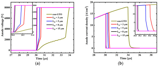
Figure 7. (a) Voltage and (b) current waveforms during turn-off process.
For the NF-RC-GTO, the device initially operates in BJT mode until the current reaches a level high enough to trigger the switch to GTO mode operation. This implies that the conductance modulation effect in the drift region is not fully activated, indicating that the concentration of injected non-equilibrium carriers in this region is lower than in conventional GTOs. Consequently, fewer carriers need to be extracted from the drift region during the turn-off process, resulting in a significantly reduced turn-off time compared to standard GTO devices.
Figure 8 displays the distribution of electron and hole concentrations in the drift region along the device’s vertical direction during normal turn-on at 15 A/cm2. The carrier concentration distribution for the NF-RC-GTO is observed to be in the range of 1 × 1016 cm−3, markedly lower than that of the con-GTO. This reduced carrier concentration is the fundamental reason behind the NF-RC-GTO’s rapid turn-off speed.
Therefore, the NF-RC-GTO possesses the potential for faster turn-off when the current to be switched off is not excessively high. The transition point from BJT to GTO mode in the device is indicated by a sudden increase in the slope of the IV curve.
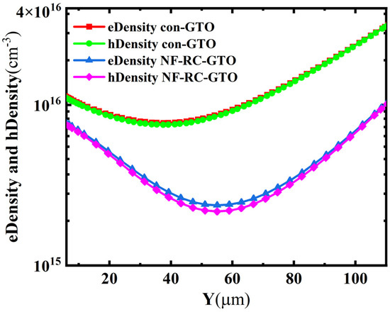
Figure 8. Electron and hole density profiles in the drift region of con-GTO and NF-RC-GTO along the device’s vertical direction during normal turn-on at 15 A/cm2.
Generally, GTOs are characterized by stringent shutdown conditions and high turn-off losses. Figure 9 illustrates the correlation between the turn-off time and turn-off energy loss of the NF-RC-GTO and LD at 8000 V and 15 A/cm2, along with a comparison to traditional GTOs.
The figure indicates a decrease in both turn-off time and loss as the LD value increases. Notably, when LD exceeds 8 µm, there is a plateau in both turn-off time and loss, with minimal further changes observed. In comparison to standard GTOs, the turn-off time of the NF-RC-GTO is reduced by over 80%, and the turn-off loss is cut by more than 85%. These findings confirm the NF-RC-GTO’s enhanced capability in reducing both turn-off time and loss, particularly in operations involving lower currents.
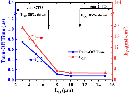
Figure 9. Turn-off time and turn-off energy of NF-RC-GTO at different LD.
4. Conclusions
In summary, we have proposed a SiC NF-RC-GTO design, incorporating an N-float layer at the cell’s bottom. Experiments conducted with TCAD simulation software have shown that an optimal setting of the NF structure’s shape and doping concentration parameters can significantly reduce the snapback effect. When the thickness of the NF structure exceeds 4 µm and the doping concentration is set to 2 × 1014 cm−3, the snapback effect is completely eliminated.
Furthermore, the breakdown voltage of the proposed NF-RC-GTO has been improved by 11.4% compared to conventional GTOs. More importantly, at specific low current densities, it can reduce turn-off time by 80% and turn-off losses by 85%, indicating this design’s significant potential in reducing losses. Our next step in the research plan involves studying the thermal management capabilities of the NF-RC-GTO and investigating the manufacturing process flow of the NF-RC-GTO.
Authors
Chengcheng Wu ,Juntao Li, Zhiqiang Li, Lin Zhang, Kun Zhou, Xiaochuan Deng.
Original – MDPI
-

STMicroelectronics announced a collaboration with Compuware Technology Inc, (Compuware), a leading provider of high-efficiency power supplies, on a reference design for server power using ST’s industry-leading silicon carbide (SiC), galvanic isolation, and microcontroller technologies. This reference design provides unparalleled power-supply options for digital power converter applications including server, datacenter and telecom power.
As demand for digital services continues to grow, fueled by Artificial Intelligence (AI), 5G, and the Internet of Things (IoT), keeping power usage under control is an important piece of the sustainability puzzle for data centers. The STDES-3KWTLCP reference design is perfect for a 3kW and higher wattage CRPS (Common Redundancy Power Supply) server power supply. This technical advancement comes with superior efficiency, faster switching, reduced energy losses, and better thermal management capabilities. In addition, this total system solution shortens time-to-market.
Compuware stands as a global power supply leader, holding the world record for the highest number of 80 PLUS Titanium certifications, ensuring unparalleled power efficiency. Engineered for excellence, Compuware power solutions are the ideal choice for HPC, AI, Deep Learning, Cloud, and advanced applications. With high power density, it optimizes space usage without compromising reliability and efficiency, setting a new performance standard in demanding computing environments.
“Combining ST’s latest SiC MOSFET, galvanic isolation, and microcontroller technologies with Compuware’s leading-edge power energy expertise is helping Compuware unleash our design creativity to develop high-density and -efficiency solutions. Now we can achieve 89W/in.3 power density, a small size, and high power output, this reference design is a great choice for power-hungry, high-performance computing applications,” according to Robin Cheng, Vice President at Compuware.
“With a focus on the Industrial market, ST’s Power & Energy Competence Center provides low-power, mid-power, and high-power solutions with the most advanced ST technologies to our customers, and this reference design- STDES-3KWTLCP can help our customers increase energy efficiency and reduce time-to-market using ST’s efficient and reliable power solutions,” said Eric Chou, Head of Power & Energy Competence Center at STMicroelectronics.
Original – STMicroelectronics
-
Heraeus is making a multi-million-euro investment in Compound Semiconductor (Xiamen) Technology Co. (CSMH), a China-headquartered material supplier of premium industrial diamond. This strategic partnership aims to drive innovations in the semiconductor industry by leveraging diamond’s unique thermal conductivity and electrical insulation properties.
Heraeus signed an investment agreement with CSMH and the deal is expected to close in several weeks. As part of the agreement, Heraeus will hold a stake in the company and receive a seat on the board of directors.
Single-crystal diamond is ultra-wideband gap (UWBG) semiconductor material with the highest known thermal conductivity, surpassing existing thermal solutions such as copper by several times. Typical silicon has a thermal conductivity around 140 W/(m-K), copper is about 400 W/(m-K), and diamond has a much higher thermal conductivity up to 2200 W/(m-K). This allows heat to be dissipated more efficiently, enabling high-performance components to endure with maximum efficiency.
In addition to its superior heat dissipation properties, diamond also withstands extremely high voltages without causing an electric breakdown. This is critical for advancing miniaturization, efficiency, and robustness in power electronics.
“This investment reinforces Heraeus’ commitment to cutting-edge material start-ups and emphasizes its strategic focus on the semiconductor market. With CSMH’s outstanding diamond wafer technologies, we expect to set new standards to accelerate AI and cloud computing, as well as revolutionize inverter architecture for EVs,” said Dr. Steffen Metzger, member of the Heraeus Executive Board.
CSMH’s core business includes the production of polycrystalline and large-sized monocrystalline diamonds, which are particularly important for high-end applications in the semiconductor industry. With already 40 patents – consisting of 23 invention patents and 17 utility models – the company has successfully established itself as an innovator and technical specialist.
“We are very excited to partner with a global industry leader like Heraeus to realize our vision to be the world’s advanced compound semiconductor material provider. Being coined as ‘the ultimate semiconductor’, diamond has many excellent performance parameters such as high pressure resistance, large radio frequency, and high-temperature resistance,” noted Zhang Xing, CEO of CSMH. “The expertise that Heraeus has in global market resources, technology insights, and industrial-scale production of advanced materials will empower CSMH to promote diamond for more applications in the near future.”
Due to its exceptional physical and chemical properties, diamond’s other prominent application includes quantum sensors, optics/detection and high-power lasers, among others. CSMH’s target customers include major players in aerospace, power electronics, optical communication, Artificial Intelligence, photovoltaics, electric vehicles, and sensors.
Industrial diamonds can be produced in a matter of weeks, at a lower cost and with greater environmental friendliness. The cooperation with CSMH aligns with Heraeus’ vision of co-developing next-generation semiconductor solutions and preparing them for use. The combination of CSMH’s specialized expertise in diamond materials and Heraeus’ global market access promises a successful expansion into international markets.
Original – Heraeus
-
 LATEST NEWS / SiC / WBG
Axcelis Technologies to Deliver Purion M™ SiC Implanters to Several Power Device Chipmakers in China
March 20, 2024
2 Min ReadAxcelis Technologies, Inc. announced multiple shipments of the Company’s Purion M™ SiC medium current implanter to several leading power device chipmakers located in China. The systems, which shipped in the first quarter, will be used for 150mm production of silicon carbide power devices supporting automotive, industrial, energy, and other power intensive applications.
President and CEO, Russell Low commented, “We look forward to supporting our customers as they expand their manufacturing capabilities in this growing silicon carbide power device segment. To meet market demand, chipmakers need to maximize their yield and add capacity, while meeting a range of technical challenges unique to power devices. The Purion M SiC Power Series platform’s common and flexible architecture, coupled with its uniquely differentiated high temperature capability, makes it ideally suited for this expanding application.”
Executive Vice President of Marketing and Applications, Greg Redinbo added “The Purion M SiC tool provides customers an implanter with a broad dose and energy range perfect for the early phases of a fab production ramp. The Purion M SiC sets the stage for the future introduction of the Purion H200™ SiC and Purion XE™ SiC. Use of the full Purion Power Series family enables higher fab productivity, lower cost of ownership and the ability to manufacture more advanced silicon carbide power devices.”
Original – Axcelis Technologies
-
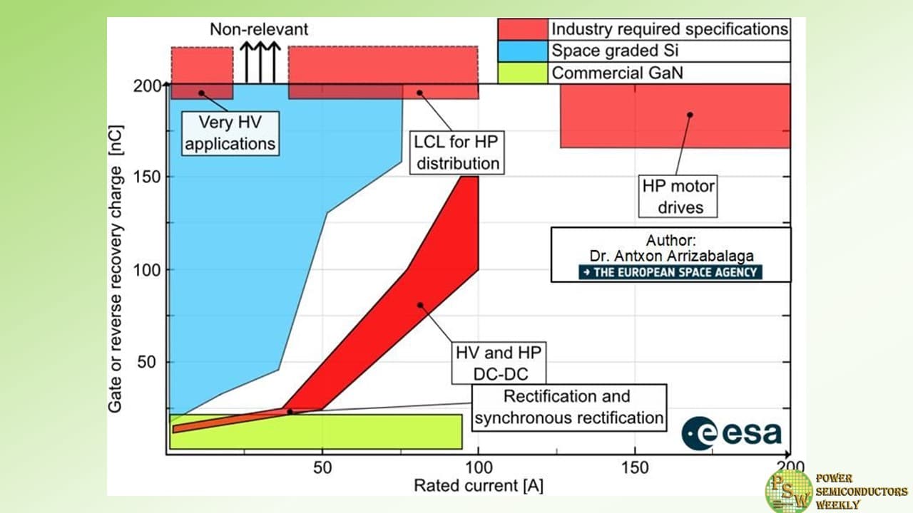
Recently the European Space Agency (ESA) started its search for the technological advantage to improve their systems. Lead by research fellow Dr. Antxon Arrizabalaga, the project is aimed at studying the latest semiconductor technologies and exploring the impact they can have in the future of the space industry.
During its research, Dr. Antxon Arrizabalaga is looking forward to answer the following questions:
- Which are the next system-level figures the space power industry wants to achieve?
- Can the wide bandgap semiconductors help to achieve these figures?
- Which semiconductor ratings are demanded by the space power industry for each application?
At the moment the research project lead by Dr. Arrizabalaga is focusing on the silicon carbide (SiC) power semiconductor devices, as they are better suited for the requirements of the high-power applications. The team has already had several meetings with the main European space power companies discussing the points of interest mentioned above.
As a result, ESA received rich feedback with industry requirements and new ideas. And as anticipated, most of the companies are looking to the ways to increase power of their systems.
Thus, the following applications were mentioned the most:
- Latching current limiters (LCL) for high power distribution
- High-voltage (HV), increasing the traditional bus voltage, and high-power (HP) DC-DC converters
- Rectification and synchronous rectification
- HP motor drives
- Very HV applications, around and over 1 kV
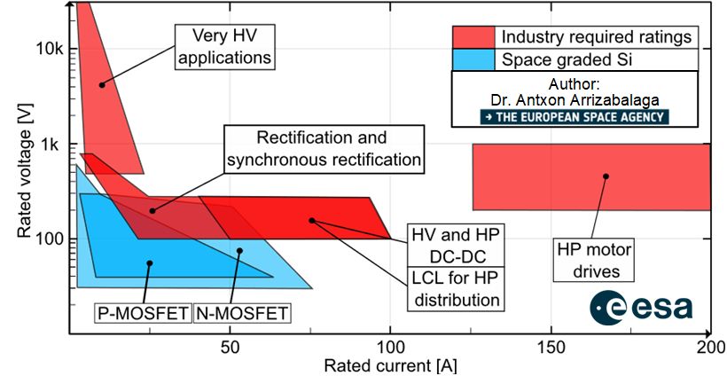
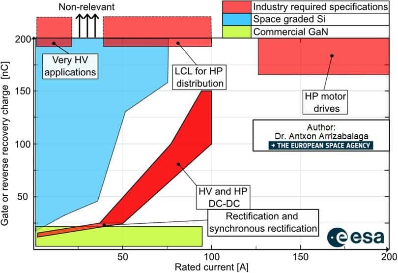
Figure 1. The ratings of the semiconductor devices required by the industry for each application
According to Dr. Arrizabalaga, ESA classifies innovations in three categories, according to the degree of innovation they bring when compared to the state-of-the-art:
- Enhancing. It brings a substantial improvement to the state-of-the-art system.
- Based on a technology replacement
- For SiC devices it means replacing the Si devices in an existing application and optimizing the system to get system-level benefits
- Low risk, development time and cost for manufacturers
- Straightforward adoption by industry and high probability of success
- Enabling. It will allow a new feature, new application, or even a new mission.
- Critical technologies for a certain feature, application or mission
- For SiC devices it means that without the adoption of such devices, the new desired feature, application or mission is no longer possible
- Medium-high risk for manufacturers, higher development cost and effort, since it has never been done before
- More challenging adoption by industry, and lower probability of success
- Game-changing. It promises to bring entirely new capabilities (not considered for this study).
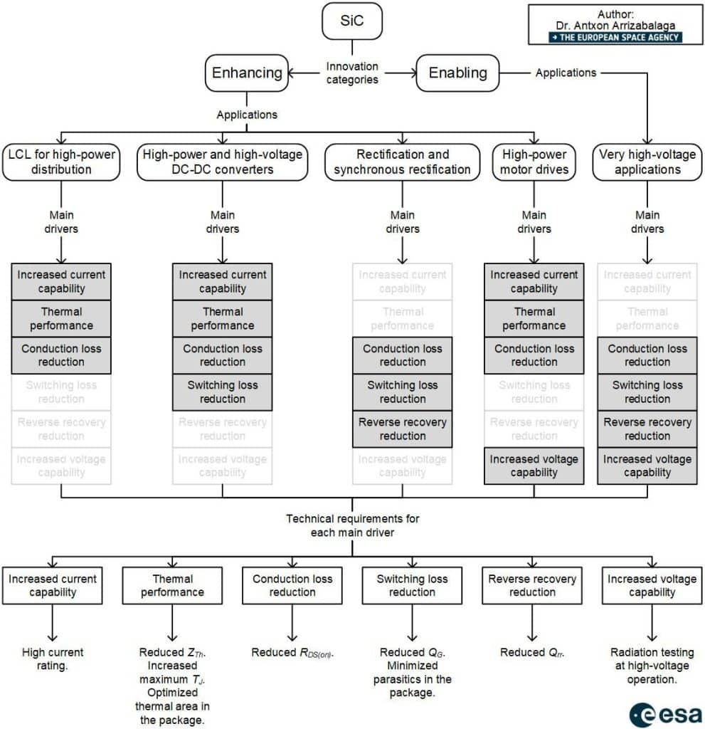
Figure 2. Classification of the applications mentioned by the industry and the main drivers needed to be optimized for each application.
The European Space Agency research team is looking forward to support the successful adoption of the wide bandgap (WBG) power semiconductor devices by the European space power industry, giving the European industry a competitive edge.
Original – Dr. Antxon Arrizabalaga
-

On 18 March 2024, Infineon Technologies AG successfully completed its Share Buyback Program 2024, announced on 26 February 2024 in accordance with Article 5(1)(a) of Regulation (EU) No 596/2014 and Article 2(1) of Delegated Regulation (EU) No 2016/1052.
As part of the Share Buyback Program 2024, a total of 7,000,000 shares (ISIN DE0006231004) were acquired. The total purchase price of the repurchased shares was € 232,872,668. The average purchase price paid per share was € 33.27.
The buyback was carried out on behalf of Infineon by an independent credit institution via Xetra trading on the Frankfurt Stock Exchange, serving the sole purpose of allocating shares to employees of the company or affiliated companies, members of the Management Board of the company as well as members of the management board and the board of directors of affiliated companies as part of the existing employee participation programs.
Original – Infineon Technologies
