-
SemiQ will showcase its latest SiC power solutions and recently launched Known-Good-Die (KGD) screening process at PCIM Europe 2024 in Nuremberg from June 11-13, 2024.
During the event SemiQ will debut the latest addition to its QSiC™ family of high-speed-switching MOSFET half-bridge modules in S3 packages, which offer enhanced design flexibility and performance in current applications.
Featuring industry-standard 62mm footprints and standing at 26.3mm in height, the new power modules address the size, weight and power demands of challenging applications, ranging from induction heaters, welding equipment and uninterruptible power supplies (UPS) to photovoltaic and wind inverters, energy storage systems, high-voltage DC-DC converters and battery charging systems for electric vehicles (EVs). They are available in 600A (GCMX003A120S3B1-N) and 400A (GCMX005A120S3B1-N). Visitors will also be able to see SemiQ’s QSiC family of 1200V modules in SOT-227, half-bridge and full-bridge options.
Attendees visiting SemiQ’s stand at Alfatec’s booth (Hall 7, 418) will have the unique opportunity to learn more about the recently launched Known-Good-Die (KGD) screening program and see SemiQ’s MOSFET bare die on Known-Good-Die UV tape array for the first time. The KGD process delivers high-quality, electrically sorted and optically inspected advanced SiC MOSFET technology ready for back-end processing and direct die attachment.
“We’re thrilled to participate at PCIM, a significant event in the power electronics industry,” said Dr. Timothy Han, President of SemiQ. “With the expansion of our QSiC family, our goal is to offer a comprehensive, high-performance SiC portfolio across various sectors and offer customized solutions for cutting-edge designs. Our continued dedication to rigorous testing and quality assurance, delivering unmatched reliability, is embodied in our new KGD program which we will be demonstrating at the event.”
Founded in 1979, PCIM Europe stands as the pinnacle exhibition and conference for power electronics and its applications. Held annually in Nuremberg, the event attracts industry specialists and academia from around the globe, serving as the platform where new trends, technologies, and developments are first unveiled to the public.
Schedule a meeting with the SemiQ team right away using online calendar here or email at media@semiq.com.
Original – SemiQ
-

X-FAB Silicon Foundries SE, the leading analog/mixed-signal and specialty foundry, has updated its XP018 high-voltage CMOS semiconductor fabrication platform with new 40V and 60V high-voltage primitive devices, which feature an extended SOA for improved operational robustness.
These 2nd generation high-voltage primitive devices exhibit up to a 50% reduction in RDSon figures compared to the previous version. This offers an alternative which is better positioned to address certain key applications – particularly where devices’ footprints need to be reduced and unit costs minimized.
The XP018 platform is a modular 180nm high-voltage EPI technology solution, based on a low mask count 5V single-gate core module. It supports an extended temperature range of -40 to 175°C and offers a wide range of optional devices and modules, including high-gain bipolar devices, standard and high-capacitance MIM capacitors, multi-threshold (Vt) options, Schottky diodes, and depletion devices.
The platform is supported by high-reliability automotive NVM solutions, such as embedded Flash, EEPROM, and OTP, making it specifically designed for cost-sensitive and robust automotive, industrial, and medical applications.
In addition to the new 40V/60V devices, the platform has been enhanced by the inclusion of 5.3V Zener diodes. The new low leakage Zener diode is designed to effectively protect the gate oxide in critical applications, such as Wide Bandgap gate driver applications. Furthermore, there are also new isolated drain high-voltage devices up to 24V and a new 1.8 V medium Vt option on offer.
Tilman Metzger, Product Line Manager for High-Voltage at X-FAB, comments: “With this update of our XP018 platform we are demonstrating X-FAB’s commitment to enhancing established technologies. XP018 has been in production for more than a decade and still sees widespread adoption for new designs from our focus market segments: automotive, industrial and medical. The new competitive high-voltage devices and updates will enable our customers to implement more innovative and cost-effective products. Designers utilizing the new XP018 primitive devices have access to comprehensive PDK support across major EDA platforms like Cadence, Siemens EDA, Synopsys, ensuring seamless integration and optimization for a range of applications.”
A new medium Vt standard cell library is scheduled to be released in Q3 2024. Further details on the XP018 platform can be accessed by going to: www.xfab.com/technology/high-voltage
Original – X-FAB Silicon Foundries
-

DISCO Corporation has developed a process for diamond wafer manufacturing that applies the KABRA process, an ingot slicing method using laser technology. This process contributes to increasing the diameter of diamond wafers.
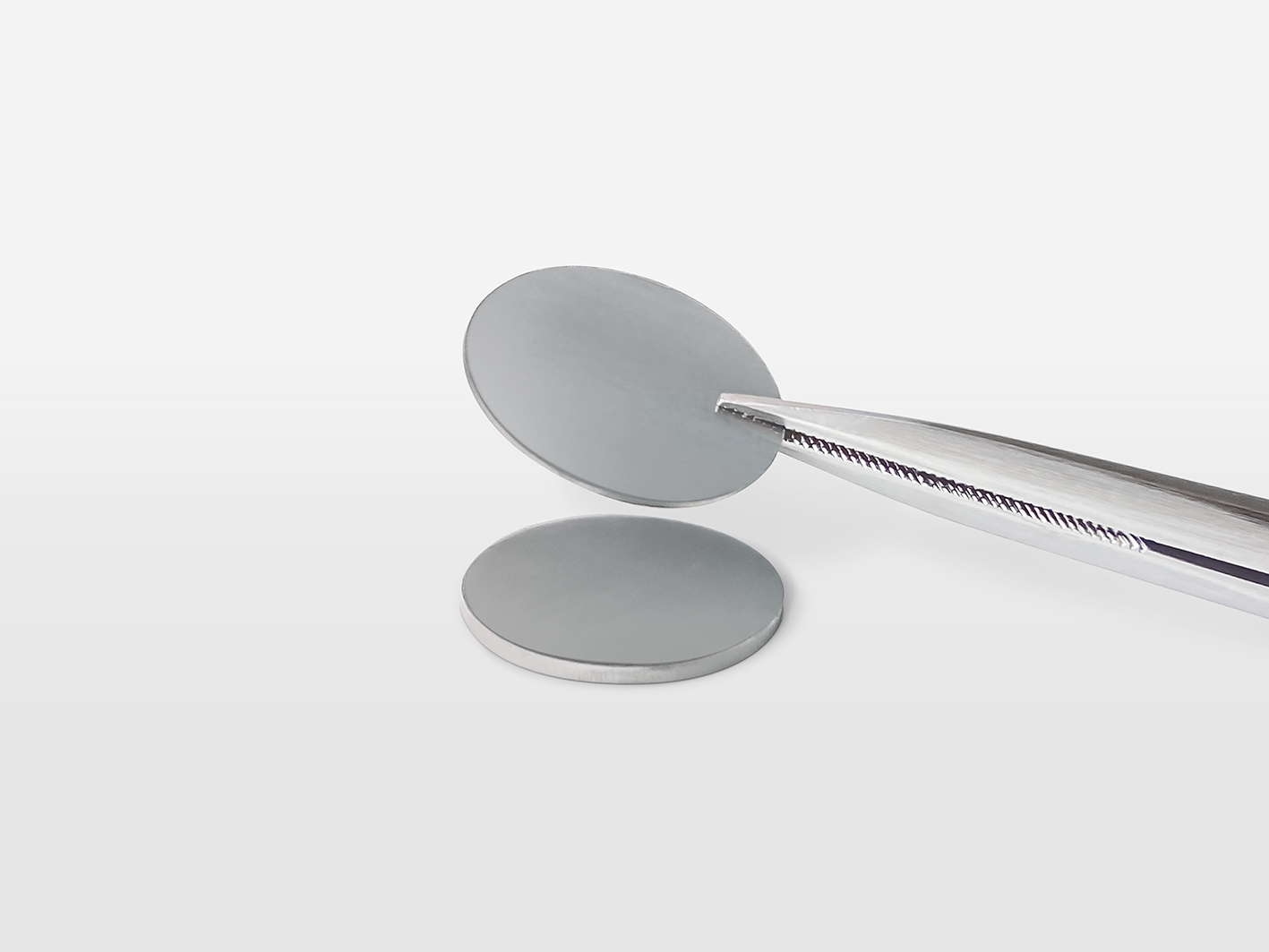
Diamond is often called the “ultimate semiconductor material” due to its superior material characteristics compared to Si, SiC, and GaN. In particular, as diamond has excellent insulation strength and heat conductivity, it is expected to be a good material for power semiconductors, and device development is underway at various research institutes.
On the other hand, as it is an extraordinarily hard material, it came to be known that it is difficult to process mechanically. Therefore, laser became the general method used to slice wafers from a diamond crystalline ingot. However, with the conventional laser slicing method, as the ingot is processed from the sidewall, there was a limitation on the ingot diameter, and it was difficult to increase it.
With KABRA slicing, there is no limitation on the ingot diameter as the laser is irradiated from the upper surface of the ingot, making it possible to increase the ingot diameter.
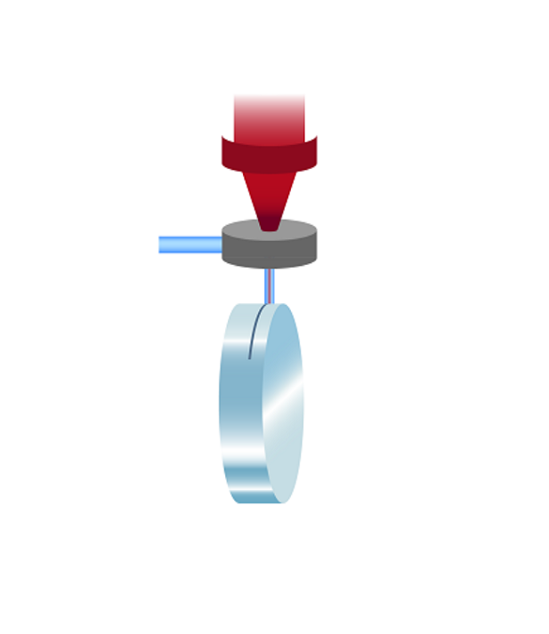
Figure 1: Conventional slicing method using laser

Figure 2: KABRA for diamond processing
Features:
- Supports large-diameter ingots exceeding Φ50 mm
With the conventional method where the laser is irradiated from the sidewall of an ingot (Figure 1), the largest supported diameter was approx. Φ30 mm, but with the KABRA method (Figure 2), as the laser is irradiated from the upper surface of the ingot, there is no limitation on the ingot diameter. - Splitting wafers with a thickness of 100 µm or less is possible
By irradiating the laser at a shallow depth from the upper surface of the ingot, it is possible to split thin wafers. Therefore, a larger number of split wafers can be expected compared to the conventional method. - Achieves equivalent or higher throughput compared to the conventional method
The splitting speed is equal to or faster than the conventional method, achieving lower processing costs.
In addition, 45 patents related to this technology have been registered. Test cuts are available. Contact a DISCO sales representative.
Original – DISCO
- Supports large-diameter ingots exceeding Φ50 mm
-

Alpha and Omega Semiconductor Limited (AOS) will showcase its expanding line of advanced power management solutions at PCIM 2024. Designed to meet the dynamic, important power management challenges in several key application areas and markets, the AOS products highlighted at PCIM include:
- New Silicon Carbide (SiC) MOSFET Announcement at PCIM: Supporting the needs of a wide range of automotive and industrial applications, AOS will introduce three new advanced package options for its latest Gen2 SiC MOSFET line. The new packages comprise a surface mount topside cooling option with a Kelvin source that meets the needs of the most power-dense advanced designs. It will also be announced that an AEC-Q101-qualified surface mount package will be in the standard D2PAK-7L footprint. The third package is a half-bridge module that provides an excellent solution for the high power industrial solar and charging station markets. The announcements will detail how these packages support AOS’ comprehensive line of SiC MOSFETs from 10mOhm to 500mOhm and voltages from 650V to 1700V.
- New Motor Drive Announcement at PCIM: AOS will announce a new range of 60V and 100V drivers for power tools, outdoor garden equipment, and e-mobility applications, including a 100V half bridge, a 100V 3-phase, and a 60V 3-phase. These products all support 100 percent duty cycle operation, and demo boards using AOS motor drivers and MOSFETs will be featured in the AOS booth.
- Power Supply and Renewable Energy: A significant solution in AOS’ growing High Voltage Super Junction MOSFET portfolio is its industry-leading optimized αMOS5™ 600V to 700V Super Junction MOSFETs that help designers achieve efficiency and density goals while satisfying budget goals. Featuring fast switching, a robust UIS/body diode, and ease of use, these state-of-the-art MOSFETs meet the latest server, telecom rectifier, solar inverter, EV charger, gaming, PC, and universal charging/PD design requirements. The newly released AONA66916, a 100V AlphaSGT™ MOSFET, delivers industry-leading Rthjc-top and Rthjc-bottom thermal resistances. A compact DFN 5×6 double-sided cooling package offers improved thermal designs in demanding telecom, solar, and DC-DC converter applications.
- Automotive and E-mobility: In AOS’ increasing line of automotive MOSFETs, the new automotive grade 80V (AOTL66810Q) and 100V (AOTL66912Q) MOSFETs in the TOLL package are designed to achieve the highest current capability. The AOS TOLL package utilizes advanced clip technology to achieve a high in-rush current rating and very low package resistance and inductance, enabling improved EMI performance compared to other TOLL packages based on standard wire-bonding technology packages. These new automotive-grade MOSFETs help designers meet the power requirements in electric vehicles, battery management systems (BMS), and high-performance inverters (BLDC motors) for e-mobility.
- Intelligent Power Modules, Mega IPM7: AOS has integrated its latest RC IGBT and high-voltage gate driver into the world’s most compact package design, capable of delivering mega power of up to 100W in motor control applications. The portfolio covers 600V / (1A−3A) in a variety of package options (Mega IPM-7D, IPM7DT, IPM-7E) that are ideal solutions for a broad array of design requirements.
- Poster Presentation: Jong-Mu Lee, Ph.D. and director of AOS IGBT and Module Product Lines, will present SiC-IPM for Compact and Energy Efficient in the Intelligent Power Modules session on Tuesday, June 11, at 15:30.
Original – Alpha and Omega Semiconductor
