
-

GlobalFoundries announced the appointment of industry and company veteran, Kay Chai (KC) Ang, as president of Asia and Chairman of China. With over 30 years of semiconductor foundry experience, Mr. Ang will lead new business development and strategic partnerships across Asia with a focus on China.
Mr. Ang joined GF in 2010 and has served in a variety of senior leadership roles for the company including most recently as Chief Manufacturing Officer with responsibility for GF’s global sites as well as previously as head of all GF’s Singapore operations.
Prior to joining GF, Mr. Ang held senior leadership positions at Chartered Semiconductor Manufacturing, including Senior Vice President of Sales and Marketing with responsibility for global sales, marketing, services, customer support and regional business operations.
Mr. Ang has been a key player in the growth of Singapore’s chip industry. He serves on the Board of the National Research Foundation in Singapore and is the Chairman of the SEMI Southeast Asia Regional Advisory Board.
“At GF, we leverage our global footprint to provide our customers with the secure, essential chips they need, where they want them produced,” said Niels Anderskouv, chief business officer at GF. “Given his more than 30 years experience coupled with his long-standing relationships with some of Asia’s most senior semiconductor industry leaders, KC is the ideal leader to drive customer engagements and partnerships across Asia and accelerate GF’s business growth within the China market in particular.”
“I am excited about this next stage of my career. I am looking forward to partnering with my commercial, technical and product management colleagues to expand GF’s relationships and be a trusted, dependable partner for our customers,” said KC Ang, president, Asia & Chairman, China at GF.
“The differentiated technology solutions that we offer combined with our manufacturing excellence, especially in key end markets such as automotive, make us a perfect partner for fast growing customers in Asia. In addition, we are responding to many of our existing multi-national customers who are looking for ways to partner with GF to serve the growing demands of their Chinese end customers with high quality manufacturing and essential chip technologies.”
Original – GlobalFoundries
-

Transphorm, Inc. announced that its PCIM 2024 showcase will underscore its ability to outperform competitive wide bandgap technologies in higher power systems. For example, Transphorm’s normally-off d-mode SuperGaN®platform delivers higher electron mobility resulting in lower crossover losses versus Silicon Carbide—making it more a cost-effective, higher performing solution for various electric vehicle, datacenter/AI, infrastructure, renewable energy, and other broad industrial applications. To learn more, visit Transphorm during PCIM in Hall 7, Stall 108 during June 11 to 13, 2024.
Transphorm SuperGaN FETs are in production in a wide range of customer products crossing the power spectrum from low 45 W power adapters to higher power 7.5 kW PSUs. Many of these customer products are the first publicly recognized GaN-based systems of their kind and uniquely demonstrate advantages enabled only by the SuperGaN platform.
Examples include the previously mentioned liquid-cooled 7.5 kW PSU for mission-critical datacenter/blockchain applications; a 2.7 kW server CRPS with > 82 W/in3 power density (highest in any GaN power system available today); and 2.2 kW and 3 kW rack-mount 1U uninterruptible power supplies (UPSes). These design wins illustrate Transphorm’s ability to drive GaN into the various application markets composing an estimated GaN TAM of $8 billion by 2028.
In addition to real-world customer products, Transphorm continues to lead in technological achievements having recently demonstrated a 5 microsecond short-circuit withstand time, a bidirectional four-quadrant switch, and a 1200 V GaN-on-Sapphire device.
On-site demonstrations will include Transphorm solutions for 2- and 3-wheeler electric vehicle chargers along with customer PSUs for renewable energy systems, data centers, and more.
Speaking Engagement
Learn more about how Transphorm’s GaN solutions outperform competitive technologies and enable cross-industry innovations during the Bodo’s Power Systems session.
Panel: GaN Wide Bandgap Design, the Future of Power
Speaker: Philip Zuk, Senior Vice President, Business Development and Marketing
Date: June 12
Time: 2:20 – 3:20 p.m. CEST
Location: Hall 7, Stall 743Original – Transphorm
-
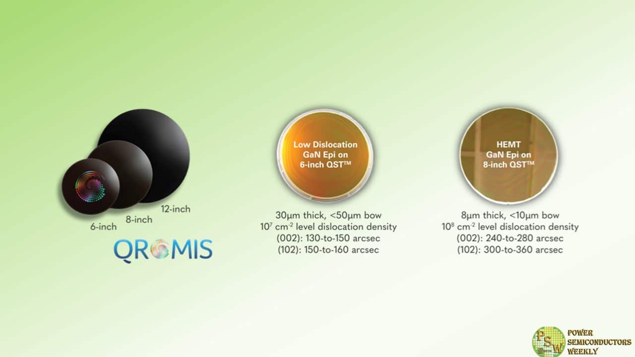
Qromis, Inc. brings a revolutionary, high performance substrate solution for large-diameter GaN epi and device wafers. Rather than solving incremental scale and performance challenges of conventional substrates for WBG semiconductors, QST™ (Qromis Substrate Technology) has been developed and validated as a disruptive solution, with cross-functional optimization.
In this approach, the key properties of substrate material such as stress, lattice mismatch, thermal stability and shape control are engineered independently for the best fit with GaN epitaxial and device layers, as well as with different device architectures and performance targets. QST™ materials layers are integrated together in the conventional semiconductor fab with a simple manufacturing flow.
The resulting large diameter substrates (6-inch, 8-inch, 12-inch or beyond) are capable of supporting from a few to tens of microns of high-quality GaN epitaxy, from which unique, high performance and low cost GaN device structures are fabricated.Qromis is designing reference devices for device manufacturers to demonstrate the benefits of the groundbreaking QST™ technology. These devices exploit key advantages of QST™ over other substrate solutions:
– High quality and stress-free GaN,
– Ability to deposit thick, bulk-like GaN epi layers on large diameter substrates,
– Low defectivity, eliminating a major limitation to performance and scalability.
With these distinct features, designers can now break free from the current technological limitations of GaN process technologies and develop advanced device architectures for lateral and vertical device designs of light emitters, switches, rectifiers, as well as monolithic and integrated circuits.Qromis, Inc., established in March 2015 and located in Silicon Valley, California, is a privately held fabless technology innovator focusing on energy efficient and high performance wide bandgap (WBG) semiconductor materials and device solutions which dramatically reduce global energy use and consumption. The Company is poised to become one of the premier players in the rapidly growing, multi-billion dollar WBG industry with its disruptive and validated solutions in substrate and device technologies, which enable an unmatched cost, performance, and application scale. Markets served include power electronics, light emitting diodes (LEDs), advanced displays, and RF electronics, and other emerging high performance and energy efficient applications.
As a fabless company, Qromis is driving the commercialization of its unique solutions in conjunction with its foundry network. The Company and its foundry partner offer WBG device foundry services, as well as access to advanced and novel process technology platforms, for its customers and partners.To learn more about Qromis and its substrate technology, join the International Conference on Compound Semiconductor Manufacturing Technology which takes place May 20-23, 2024 in Tucson, Arizona.
Original – Qromis