-
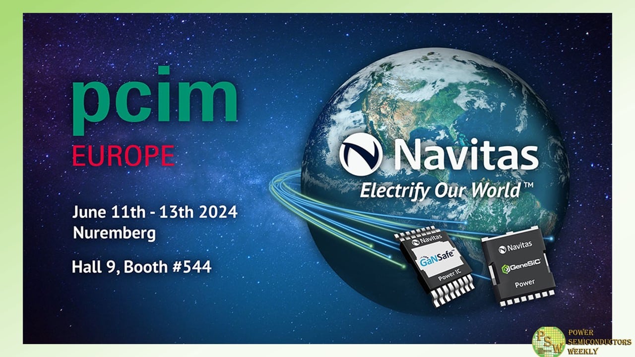
Navitas Semiconductor invites visitors to experience “Planet Navitas” at PCIM 2024 (June 11th-13th) and see how industry-leading GaN and SiC solutions deliver optimal performance in a broad array of fast-growing markets and applications from 20 W to 20 MW.
Aligned with Navitas’ mission to “Electrify Our World™”, the “Planet Navitas” booth invites visitors to discover how next-gen GaN and SiC technology enable the latest solutions for fully-electrified EV transportation, AI data centers, industrial compressors, drives, and robotics plus renewable energy sourcing and storage.
Each example highlights end-user benefits such as increased portability, longer range, faster charging, and grid independence, along with a focus on how low-carbon-footprint GaN and SiC technology can save over 6 Gtons/yr CO2 by 2050.
“PCIM is a key event in the power-electronics calendar,” says Alessandro Squeri, Navitas’ senior director for European sales. “Complementary GaNFast and GeneSiC portfolios, with comprehensive, application-specific system design support, accelerate customer time-to-market with sustainable performance advantages. ‘Planet Navitas’ represents the very real, inspiring implementation of GaN & SiC that makes up a $1.6B identified customer pipeline as part of a vast $22B/year market opportunity.”
Major technology updates and releases include GaNSafe™ – the world’s most-protected, most reliable, and highest-performance GaN power, Gen-4 GaNSense™ Half-Bridge ICs – the most integrated GaN devices, and Gen-3 Fast GeneSiC power FETs – for game-changing motor drive and energy-storage applications.
In addition to the exhibition, PCIM 2024 includes peer-review technical presentations, including:
11th June, 13:00 – 14:30, Hall 10.1
- “Low-Cost High-Density 300 W / 20 V AC-DC Converter Enabled by GaN Power ICs”– Tom Ribarich, Sr. Director of Strategic Marketing, Navitas Semiconductor
- A low-cost 300 W high-density AC-to-DC converter has been designed and demonstrated to achieve >96% peak efficiency and 270 cc. The circuit topologies include a 2-phase interleaved PFC input stage, an LLC DC-DC stage, and a synchronous rectification output stage. The design includes GaN Power ICs and off-the-shelf controllers running at 300 kHz. This new design has resulted in a cased power density of 1.1 W/cc.
12th June, 15:30 – 17:00, Foyer
- Evaluation of SiC Devices for Over 500 kHz Application Based on Buck Circuit – Minli Jia, Sr. Staff Applications Engineer, Navitas Semiconductor
- This paper selects three 1200 V SiC devices of similar specifications and different manufacturers for analysis and experimental research and designs a Buck converter with an output power of 3.6 kW and a switching frequency of 600 kHz. The efficiency and heat of three SiC types were tested under the same working conditions, and the results showed that the SiC with fast turn-off characteristics and low thermal resistance was more suitable for high-frequency converter applications.
Original – Navitas Semiconductor
- “Low-Cost High-Density 300 W / 20 V AC-DC Converter Enabled by GaN Power ICs”– Tom Ribarich, Sr. Director of Strategic Marketing, Navitas Semiconductor
-

Nexperia announced that it is now offering its industry leading 1200 V silicon carbide (SiC) MOSFETs in D2PAK-7 surface mount device (SMD) packaging, with a choice of 30, 40, 60, and 80 mΩ RDSon values. This announcement follows on from Nexperia’s late-2023 release of two discrete SiC MOSFETs in 3 and 4-pin TO-247 packaging and is the latest offering in a series which will see its SiC MOSFET portfolio swiftly expand to include devices with RDSon values of 17, 30, 40, 60 and 80 mΩ in flexible package options.
With the release of the NSF0xx120D7A0, Nexperia is addressing the growing market demand for high performance SiC switches in SMD packages like D2PAK-7, which is becoming increasingly popular in various industrial applications including electric vehicle (EV) charging (charge pile, offboard charging), uninterruptible power supplies (UPS) and inverters for solar and energy storage systems (ESS).
It is also further testimony to Nexperia’s successful strategic partnership with Mitsubishi Electric Corporation (MELCO), which has seen the two companies join forces to push the energy efficiency and electrical performance of SiC wide bandgap semiconductors to the next level, while additionally future-proofing production capacity for this technology in response to ever growing market demand.
RDSon is a critical performance parameter for SiC MOSFETs because it impacts conduction power losses. However, many manufacturers concentrate on the nominal value, neglecting the fact that it can increase by more than 100% as device operating temperatures rise, resulting in considerable conduction losses.
Nexperia identified this as a limiting factor in the performance of many currently available SiC devices and leveraged the features of its innovative process technology to ensure that its new SiC MOSFETs offer industry-leading temperature stability, with the nominal value of RDSon increasing by only 38% over an operating temperature range from 25 °C to 175 °C.
Tightest threshold voltage, VGS(th) specification, allows these discrete MOSFETs to offer balanced current-carrying performance when connected in parallel. Furthermore, low body diode forward voltage (VSD) is a parameter which increases device robustness and efficiency, while also relaxing the dead-time requirement during freewheeling operation.
Original – Nexperia
-

GlobalFoundries announced the appointment of industry and company veteran, Kay Chai (KC) Ang, as president of Asia and Chairman of China. With over 30 years of semiconductor foundry experience, Mr. Ang will lead new business development and strategic partnerships across Asia with a focus on China.
Mr. Ang joined GF in 2010 and has served in a variety of senior leadership roles for the company including most recently as Chief Manufacturing Officer with responsibility for GF’s global sites as well as previously as head of all GF’s Singapore operations.
Prior to joining GF, Mr. Ang held senior leadership positions at Chartered Semiconductor Manufacturing, including Senior Vice President of Sales and Marketing with responsibility for global sales, marketing, services, customer support and regional business operations.
Mr. Ang has been a key player in the growth of Singapore’s chip industry. He serves on the Board of the National Research Foundation in Singapore and is the Chairman of the SEMI Southeast Asia Regional Advisory Board.
“At GF, we leverage our global footprint to provide our customers with the secure, essential chips they need, where they want them produced,” said Niels Anderskouv, chief business officer at GF. “Given his more than 30 years experience coupled with his long-standing relationships with some of Asia’s most senior semiconductor industry leaders, KC is the ideal leader to drive customer engagements and partnerships across Asia and accelerate GF’s business growth within the China market in particular.”
“I am excited about this next stage of my career. I am looking forward to partnering with my commercial, technical and product management colleagues to expand GF’s relationships and be a trusted, dependable partner for our customers,” said KC Ang, president, Asia & Chairman, China at GF.
“The differentiated technology solutions that we offer combined with our manufacturing excellence, especially in key end markets such as automotive, make us a perfect partner for fast growing customers in Asia. In addition, we are responding to many of our existing multi-national customers who are looking for ways to partner with GF to serve the growing demands of their Chinese end customers with high quality manufacturing and essential chip technologies.”
Original – GlobalFoundries
-

Transphorm, Inc. announced that its PCIM 2024 showcase will underscore its ability to outperform competitive wide bandgap technologies in higher power systems. For example, Transphorm’s normally-off d-mode SuperGaN®platform delivers higher electron mobility resulting in lower crossover losses versus Silicon Carbide—making it more a cost-effective, higher performing solution for various electric vehicle, datacenter/AI, infrastructure, renewable energy, and other broad industrial applications. To learn more, visit Transphorm during PCIM in Hall 7, Stall 108 during June 11 to 13, 2024.
Transphorm SuperGaN FETs are in production in a wide range of customer products crossing the power spectrum from low 45 W power adapters to higher power 7.5 kW PSUs. Many of these customer products are the first publicly recognized GaN-based systems of their kind and uniquely demonstrate advantages enabled only by the SuperGaN platform.
Examples include the previously mentioned liquid-cooled 7.5 kW PSU for mission-critical datacenter/blockchain applications; a 2.7 kW server CRPS with > 82 W/in3 power density (highest in any GaN power system available today); and 2.2 kW and 3 kW rack-mount 1U uninterruptible power supplies (UPSes). These design wins illustrate Transphorm’s ability to drive GaN into the various application markets composing an estimated GaN TAM of $8 billion by 2028.
In addition to real-world customer products, Transphorm continues to lead in technological achievements having recently demonstrated a 5 microsecond short-circuit withstand time, a bidirectional four-quadrant switch, and a 1200 V GaN-on-Sapphire device.
On-site demonstrations will include Transphorm solutions for 2- and 3-wheeler electric vehicle chargers along with customer PSUs for renewable energy systems, data centers, and more.
Speaking Engagement
Learn more about how Transphorm’s GaN solutions outperform competitive technologies and enable cross-industry innovations during the Bodo’s Power Systems session.
Panel: GaN Wide Bandgap Design, the Future of Power
Speaker: Philip Zuk, Senior Vice President, Business Development and Marketing
Date: June 12
Time: 2:20 – 3:20 p.m. CEST
Location: Hall 7, Stall 743Original – Transphorm
-
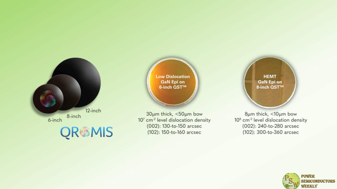
Qromis, Inc. brings a revolutionary, high performance substrate solution for large-diameter GaN epi and device wafers. Rather than solving incremental scale and performance challenges of conventional substrates for WBG semiconductors, QST™ (Qromis Substrate Technology) has been developed and validated as a disruptive solution, with cross-functional optimization.
In this approach, the key properties of substrate material such as stress, lattice mismatch, thermal stability and shape control are engineered independently for the best fit with GaN epitaxial and device layers, as well as with different device architectures and performance targets. QST™ materials layers are integrated together in the conventional semiconductor fab with a simple manufacturing flow.
The resulting large diameter substrates (6-inch, 8-inch, 12-inch or beyond) are capable of supporting from a few to tens of microns of high-quality GaN epitaxy, from which unique, high performance and low cost GaN device structures are fabricated.Qromis is designing reference devices for device manufacturers to demonstrate the benefits of the groundbreaking QST™ technology. These devices exploit key advantages of QST™ over other substrate solutions:
– High quality and stress-free GaN,
– Ability to deposit thick, bulk-like GaN epi layers on large diameter substrates,
– Low defectivity, eliminating a major limitation to performance and scalability.
With these distinct features, designers can now break free from the current technological limitations of GaN process technologies and develop advanced device architectures for lateral and vertical device designs of light emitters, switches, rectifiers, as well as monolithic and integrated circuits.Qromis, Inc., established in March 2015 and located in Silicon Valley, California, is a privately held fabless technology innovator focusing on energy efficient and high performance wide bandgap (WBG) semiconductor materials and device solutions which dramatically reduce global energy use and consumption. The Company is poised to become one of the premier players in the rapidly growing, multi-billion dollar WBG industry with its disruptive and validated solutions in substrate and device technologies, which enable an unmatched cost, performance, and application scale. Markets served include power electronics, light emitting diodes (LEDs), advanced displays, and RF electronics, and other emerging high performance and energy efficient applications.
As a fabless company, Qromis is driving the commercialization of its unique solutions in conjunction with its foundry network. The Company and its foundry partner offer WBG device foundry services, as well as access to advanced and novel process technology platforms, for its customers and partners.To learn more about Qromis and its substrate technology, join the International Conference on Compound Semiconductor Manufacturing Technology which takes place May 20-23, 2024 in Tucson, Arizona.
Original – Qromis
-

Applied Materials, Inc. reported results for its second quarter ended Apr. 28, 2024.
Applied generated revenue of $6.65 billion. On a GAAP basis, the company reported gross margin of 47.4 percent, operating income of $1.91 billion or 28.8 percent of net revenue, and earnings per share (EPS) of $2.06. On a non-GAAP basis, the company reported gross margin of 47.5 percent, operating income of $1.93 billion or 29.0 percent of net revenue, and EPS of $2.09.
The company generated $1.39 billion in cash from operations and distributed $1.09 billion to shareholders including $820 million in share repurchases and $266 million in dividends.
“Applied Materials continues to deliver strong performance in 2024, with fiscal second quarter revenue and earnings towards the high end of our guided range,” said Gary Dickerson, President and CEO.
“Applied Materials has the most enabling portfolio of materials engineering technologies for chips that underpin tectonic shifts in technology including AI, IoT, electric vehicles and clean energy, which puts us in a great position to grow along with these long-term, secular trends.”
Original – Applied Materials
-
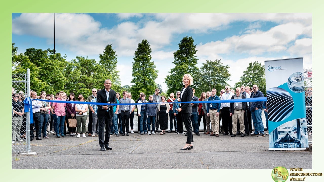
Siltronic Portland proudly announced the inauguration of its state-of-the-art solar field on May 16, 2024. This marks a milestone in the company’s commitment to sustainability and reducing its carbon footprint.
“We see sustainability not just as a duty, but as a deeply rooted conviction. It is our responsibility not only to ensure financial profits, but also to work for the sustainable development of Siltronic and the preservation of our environment for future generations. Our new solar field exemplifies our commitment to a greener and more sustainable future”, stated Claudia Schmitt, CFO of Siltronic.
Siltronic AG has implemented a climate action plan aimed at limiting global warming to 1.5 degrees Celsius, in line with the 2015 Paris Climate Agreement. The company intends to reduce its Scope 1 and 2 greenhouse gas emissions by 42 percent by 2030, using 2021 as the baseline. Additionally, Siltronic aims to achieve net zero emissions by 2045. To achieve these targets, Siltronic utilizes three main levels: enhancing energy efficiency, generating its own renewable energy, and purchasing renewable energy.
As part of the in-house generation of renewable energy, the solar field with a capacity of 1,500 MWh per year started generating electricity last week. The energy produced from this solar field could sustain almost 140 Oregon households for an entire year. It contains 2,353 panels mounted on a fixed ground mount system and spans an area of 420 feet by 250 feet. The ribbon-cutting ceremony was conducted by Claudia Schmitt, CFO of Siltronic, and Subramania Krishnakumar, President of the Portland Site.
Founded in 1978 as Wacker Siltronic Corporation, the Portland site serves as the first international location in Siltronic’s production network. In 1980, the site celebrated the inauguration of Fab 1 and commenced production of 100 mm wafers, followed by expansions to increase capacity and capability, including the addition of 150 mm wafers in the mid-1980s. In 1996, production began in Fab 2, specializing in 200 mm wafers. Throughout its history, the Portland site has received numerous awards for its dedication to efficiency and sustainability. Today, Siltronic Portland remains focused on manufacturing high-quality 200 mm wafers for customers worldwide. With approximately 400 employees, the site specializes in wafering production, offering a range of polished and epitaxial wafers.
Original – Siltronic
-
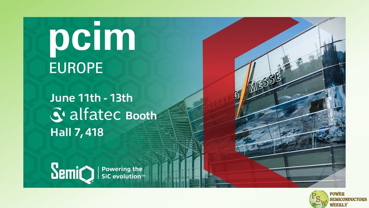
SemiQ will showcase its latest SiC power solutions and recently launched Known-Good-Die (KGD) screening process at PCIM Europe 2024 in Nuremberg from June 11-13, 2024.
During the event SemiQ will debut the latest addition to its QSiC™ family of high-speed-switching MOSFET half-bridge modules in S3 packages, which offer enhanced design flexibility and performance in current applications.
Featuring industry-standard 62mm footprints and standing at 26.3mm in height, the new power modules address the size, weight and power demands of challenging applications, ranging from induction heaters, welding equipment and uninterruptible power supplies (UPS) to photovoltaic and wind inverters, energy storage systems, high-voltage DC-DC converters and battery charging systems for electric vehicles (EVs). They are available in 600A (GCMX003A120S3B1-N) and 400A (GCMX005A120S3B1-N). Visitors will also be able to see SemiQ’s QSiC family of 1200V modules in SOT-227, half-bridge and full-bridge options.
Attendees visiting SemiQ’s stand at Alfatec’s booth (Hall 7, 418) will have the unique opportunity to learn more about the recently launched Known-Good-Die (KGD) screening program and see SemiQ’s MOSFET bare die on Known-Good-Die UV tape array for the first time. The KGD process delivers high-quality, electrically sorted and optically inspected advanced SiC MOSFET technology ready for back-end processing and direct die attachment.
“We’re thrilled to participate at PCIM, a significant event in the power electronics industry,” said Dr. Timothy Han, President of SemiQ. “With the expansion of our QSiC family, our goal is to offer a comprehensive, high-performance SiC portfolio across various sectors and offer customized solutions for cutting-edge designs. Our continued dedication to rigorous testing and quality assurance, delivering unmatched reliability, is embodied in our new KGD program which we will be demonstrating at the event.”
Founded in 1979, PCIM Europe stands as the pinnacle exhibition and conference for power electronics and its applications. Held annually in Nuremberg, the event attracts industry specialists and academia from around the globe, serving as the platform where new trends, technologies, and developments are first unveiled to the public.
Schedule a meeting with the SemiQ team right away using online calendar here or email at media@semiq.com.
Original – SemiQ
-

X-FAB Silicon Foundries SE, the leading analog/mixed-signal and specialty foundry, has updated its XP018 high-voltage CMOS semiconductor fabrication platform with new 40V and 60V high-voltage primitive devices, which feature an extended SOA for improved operational robustness.
These 2nd generation high-voltage primitive devices exhibit up to a 50% reduction in RDSon figures compared to the previous version. This offers an alternative which is better positioned to address certain key applications – particularly where devices’ footprints need to be reduced and unit costs minimized.
The XP018 platform is a modular 180nm high-voltage EPI technology solution, based on a low mask count 5V single-gate core module. It supports an extended temperature range of -40 to 175°C and offers a wide range of optional devices and modules, including high-gain bipolar devices, standard and high-capacitance MIM capacitors, multi-threshold (Vt) options, Schottky diodes, and depletion devices.
The platform is supported by high-reliability automotive NVM solutions, such as embedded Flash, EEPROM, and OTP, making it specifically designed for cost-sensitive and robust automotive, industrial, and medical applications.
In addition to the new 40V/60V devices, the platform has been enhanced by the inclusion of 5.3V Zener diodes. The new low leakage Zener diode is designed to effectively protect the gate oxide in critical applications, such as Wide Bandgap gate driver applications. Furthermore, there are also new isolated drain high-voltage devices up to 24V and a new 1.8 V medium Vt option on offer.
Tilman Metzger, Product Line Manager for High-Voltage at X-FAB, comments: “With this update of our XP018 platform we are demonstrating X-FAB’s commitment to enhancing established technologies. XP018 has been in production for more than a decade and still sees widespread adoption for new designs from our focus market segments: automotive, industrial and medical. The new competitive high-voltage devices and updates will enable our customers to implement more innovative and cost-effective products. Designers utilizing the new XP018 primitive devices have access to comprehensive PDK support across major EDA platforms like Cadence, Siemens EDA, Synopsys, ensuring seamless integration and optimization for a range of applications.”
A new medium Vt standard cell library is scheduled to be released in Q3 2024. Further details on the XP018 platform can be accessed by going to: www.xfab.com/technology/high-voltage
Original – X-FAB Silicon Foundries
-

DISCO Corporation has developed a process for diamond wafer manufacturing that applies the KABRA process, an ingot slicing method using laser technology. This process contributes to increasing the diameter of diamond wafers.
Diamond is often called the “ultimate semiconductor material” due to its superior material characteristics compared to Si, SiC, and GaN. In particular, as diamond has excellent insulation strength and heat conductivity, it is expected to be a good material for power semiconductors, and device development is underway at various research institutes.
On the other hand, as it is an extraordinarily hard material, it came to be known that it is difficult to process mechanically. Therefore, laser became the general method used to slice wafers from a diamond crystalline ingot. However, with the conventional laser slicing method, as the ingot is processed from the sidewall, there was a limitation on the ingot diameter, and it was difficult to increase it.
With KABRA slicing, there is no limitation on the ingot diameter as the laser is irradiated from the upper surface of the ingot, making it possible to increase the ingot diameter.
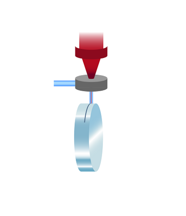
Figure 1: Conventional slicing method using laser
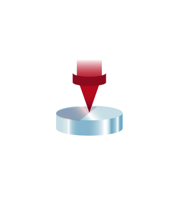
Figure 2: KABRA for diamond processing
Features:
- Supports large-diameter ingots exceeding Φ50 mm
With the conventional method where the laser is irradiated from the sidewall of an ingot (Figure 1), the largest supported diameter was approx. Φ30 mm, but with the KABRA method (Figure 2), as the laser is irradiated from the upper surface of the ingot, there is no limitation on the ingot diameter. - Splitting wafers with a thickness of 100 µm or less is possible
By irradiating the laser at a shallow depth from the upper surface of the ingot, it is possible to split thin wafers. Therefore, a larger number of split wafers can be expected compared to the conventional method. - Achieves equivalent or higher throughput compared to the conventional method
The splitting speed is equal to or faster than the conventional method, achieving lower processing costs.
In addition, 45 patents related to this technology have been registered. Test cuts are available. Contact a DISCO sales representative.
Original – DISCO
- Supports large-diameter ingots exceeding Φ50 mm
