-
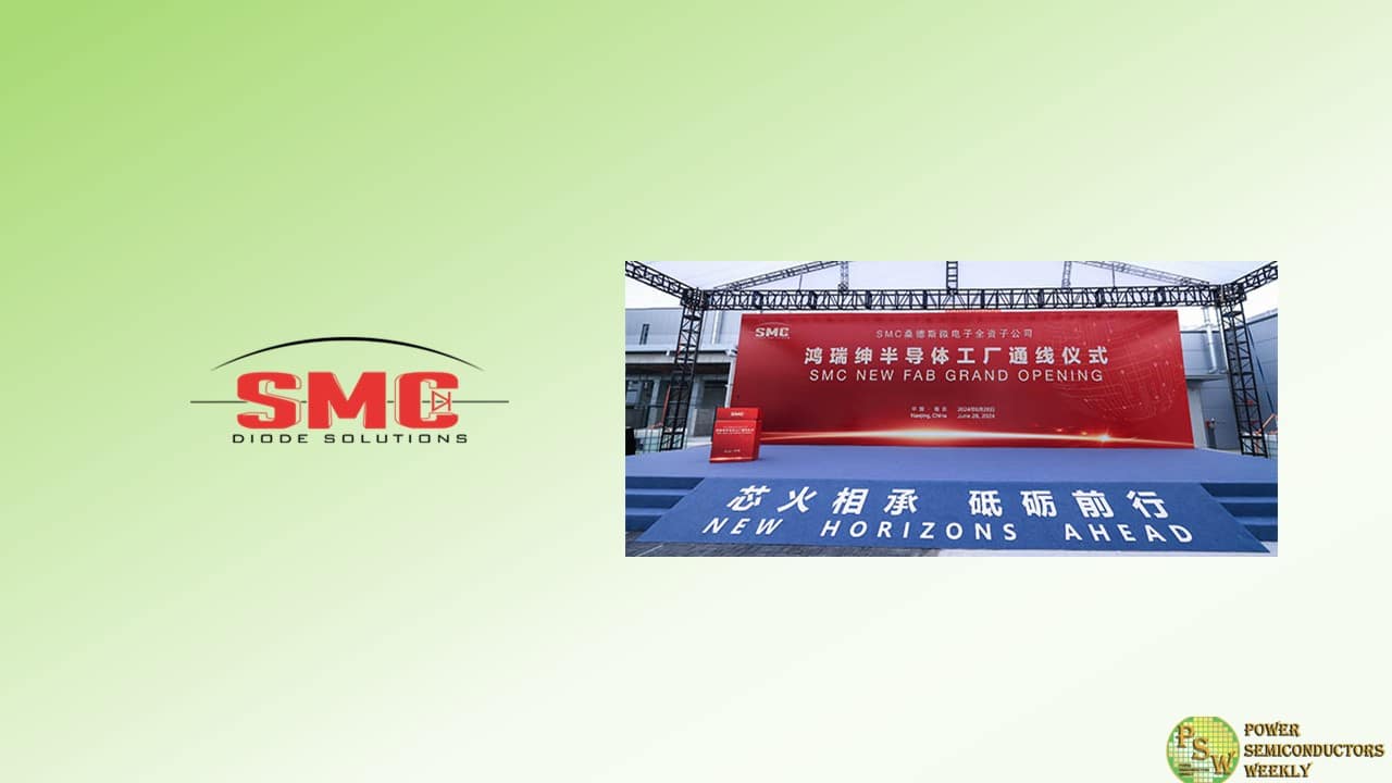
SMC Diode Solutions, an American-led semiconductor design and manufacturing company, celebrated the opening of its second power discrete fab in Nanjing, China. The new facility realized volume production only 21 months after groundbreaking in September of 2022, and will begin shipments to customers in Q4 2024 for high power and high voltage rectifiers and MOSFET 6-inch and 8-inch wafers.
This new fab marks a milestone in SMC’s growth as they further invest in the China market and the growing renewable energy sector. The new 300,000 square foot facility is set to produce 1.2 million silicon wafers and 60,000 silicon carbide wafers per year, increasing SMC’s total production by over four times. SMC’s current fab in Lukou, Nanjing currently produces 300,000 silicon wafers per year. The $3 billion RMB investment in the new fab will allow SMC to handle the end-to-end production of silicon carbide products for the first time and has created three hundred new jobs.
“As the world moves towards using more and more renewable energy, we are thrilled to now be able to participate in the sector and be part of the solution to increase green energy usage and protect our Earth. We are very excited to have our new fab up and running and we look forward to servicing our customers’ needs better with the increased capacity.” – Dr. Yunji Corcoran, SMC chairwoman and chief executive officer.
As Nanjing is also home to SMC’s current fab, the city was an advantageous choice for the new fab location. With their experienced management team, starting up the new fab was a seamless process, allowing production to begin not long after breaking ground. The city is also home to abundant resources and engineering talent, making it an ideal place for SMC to grow and expand.
Power Semiconductors Weekly team had pleasure to interview Dr. Yunji Corcoran on this occasion:
- The company history dates back to 1997. Can you tell us about some of the major milestones and your semiconductor journey so far?
Certainly. In the early stages of our company, from 1997 until about 2014, we focused on the US and South Korean markets. We were growing steadily, but remained focused on the quality of our products. From 2014 to 2019, we began to focus on active growth, but I consider this more of a preparation stage for our company’s expansion. We investigated ways to create better products and put more of our R&D efforts into new silicon and Silicon Carbide (SiC) products. We also began strengthening our salesforce globally. From 2019 on, we started shipping our new products, both silicon and SiC. Now, we have reached our most significant milestone to date: opening our second fab and quadrupling our production capabilities. We are beginning a new phase that will focus on growing our presence in the power semiconductor market.
- Today we see many semiconductor companies investing a lot of energy into the automotive, renewables, and AI applications. With a wide product line and a new wafer fab to support further expansion, what are your major areas of interest and how do you see them evolve in the coming years?
Automotive, renewables, and AI are extremely relevant markets for both our company and the overall semiconductor industry right now. AI requires a lot of power supply, so we plan to grow our power supply products in that area alongside our existing customers. Automotive and renewables are newer segments for us and the semiconductor market, but ones with incredibly high demand right now. The market is growing rapidly, so we are growing with aims to successfully compete in those areas as well.
Our plan is to focus on our growth within the power supply market and naturally expand into the sustainable energy market. As the world continues to prioritize clean energy, the demand for EV and renewable energy products will also grow. Since SiC products in particular meet the specific power needs of those applications, a rise in the use of SiC products seems likely. I suspect the semiconductor industry will play a crucial role in providing more clean energy globally, which we are excited to be a part of.
- With the new fab you plan to address both silicon and silicon carbide markets? What is your view on the growing demand for SiC and how SMC Diode Solutions plan to correspond to it?
Yes, our new fab will produce both silicon and SiC products. Our current fab produces approximately 300,000 silicon wafers per year, but our new fab has the capability to produce a total of 1,260,000 wafers per year – 1,200,000 silicon and 60,000 SiC. We are very much focused on our silicon power products and view our SiC line as a natural extension of that.
The growing demand for SiC products makes perfect sense. SiC is a material with remarkable properties. It is considered a “wide bandgap” material, which means that it requires more energy to excite electrons from the valence band to the conduction band compared to standard silicon semiconductors. As a result, it offers superior performance characteristics including higher reverse voltage capabilities and greater stability at high temperatures.
Overall, SiC-based products offer improved efficiency and reliability compared to traditional silicon counterparts. For a lot of newer applications, particularly in the sustainable energy sector, these capabilities have become more and more necessary. We see our new fab opening as a natural response to this demand, ande are increasing our capabilities to grow alongside the market.
- Today you have four major locations in China, South Korea, Germany and the USA. Do you plan to expand your network further?
Yes, definitely. We consider SMC to be a global company, and have a range of operations throughout the world, including our headquarters in China and other offices in the US, Germany, South Korea, the UK, and India. As we grow and gain customers throughout the world, we will continue to establish more locations, whether they are R&D, manufacturing, packaging, or sales offices.
- Speaking of the network and future growth opportunities. Both of your fabs are located in Nanjing. With many companies in the US already taking advantage of the CHIPS and Science Act, do SMC Diode Solutions have any considerations to join the rest and use this chance to strengthen the US presence?
It is exciting that governments are recognizing the importance of semiconductors through initiatives like the CHIPS and Science Act, and I think this will really bolster the industry as a whole. Right now, we’re focused on our manufacturing efforts in Asia, but are open to the possibility as we continue to grow.
- With the rise of the Chinese semiconductor industry and a very competitive landscape, how do you position your company and differentiate from the growing number of new entrants?
The key thing is our products. Our products stand out for their high quality and outstanding performance. Our team’s commitment to customer service really sets us apart as well.
Our company also approaches the semiconductor market from a unique perspective. As a business with global locations and leadership, we deeply understand the needs of the international market. We prioritize high quality standards that the international market demands while benefiting from relatively low overall production costs, creating an ideal product for our customers.
- We see many companies in China, Europe, the US, shifting to the vertical structure and full integration of all processes – from growing the semiconductor boules to the packaging of the final product. What are your thoughts on such an approach and do you see it applicable for your company in the future as well?
I’ve also noticed this trend in the industry. While I can see the benefits of this approach for some, I would not anticipate applying it within SMC. I believe in focusing our efforts on what we’re able to do best. We have specialized in design and manufacturing for over 25 years and plan to continue that.
We do have an existing silicon module line, so we are considering expanding into SiC modules in the future. However, for our company we believe it’s best to stay focused on the functions we currently have and prioritize delivering the highest quality product.
- And lastly, after the announcement of a new fab opening, many of your partners would be willing to engage in discussions to find out more. What trade shows or conferences in the second half of 2024 can they meet the company at?
We would love to engage in those discussions as well. You can find us with our own booth at Electronica 2024 this September in Munich, Germany and the Anaheim Electronics & Manufacturing Show (AEMS 2024) in Anaheim, California this October. We will also be attending ISCRM 2024 in Raleigh, North Carolina this fall.
More often than not, you will find someone from our company at any major semiconductor event. Feel free to contact us at sales@smc-diodes.com for any questions or check our website updates to see where you can find us next.
Original – SMC Diode Solutions
-

Axcelis Technologies, Inc. announced the establishment of new service offices in Chitose, Hokkaido and Kumamoto, Kyushu to support the Company’s expanding customer base in Japan. Both service office locations opened in June 2024.
President and CEO of Axcelis Technologies Russell Low, said, “We are proud of our growing installed base in Japan and remain focused on expanding our market share by providing customers the most innovative, enabling implant technology and support solutions to ensure their success. Our family of application specific systems address high current, medium current, medium energy and high energy implant requirements for all existing and emerging IC applications.”
Charles Pieczulewski, Axcelis Japan Country Manager, commented, “We are pleased to announce the opening of two new Japan Service centers. The proximity of both of the new offices to customers will enable localized support resources for our Purion ion implant equipment running in production. Axcelis has established business relationships with both Silicon (Si) and Silicon Carbide (SiC) semiconductor power device customers in Japan and is now positioned to support investments by Japanese customers in advanced logic production capacity.”
Original – Axcelis Technologies
-
Semiconductor manufacturer Nexperia announced plans to invest USD 200 million (appx. 184 million Euros) to develop the next generation of wide bandgap semiconductors (WBG) such as silicon carbide (SiC) and gallium nitride (GaN), and to establish production infrastructure at the Hamburg site. At the same time, wafer fab capacity for silicon (Si) diodes and transistors will be increased. The investments are jointly announced with Hamburg’s Minister for Economic Affairs, Dr. Melanie Leonhard, on the occasion of the 100-year anniversary of the production site.
To meet the growing long-term demand for efficient power semiconductors, all three technologies (SiC, GaN, and Si) will be developed and produced in Germany starting in June 2024. This means Nexperia is supporting key technologies in the fields of electrification and digitalization. SiC and GaN semiconductors enable power-hungry applications, such as data centers, to operate with exceptional efficiency and are core building blocks for renewable energy applications and electromobility. These WBG technologies have great potential and are increasingly important for achieving decarbonization goals.
“This investment strengthens our position as a leading supplier of energy-efficient semiconductors and enables us to utilize available electrical energy more responsibly,” comments Achim Kempe, COO and managing director at Nexperia Germany. “In the future, our Hamburg fab will cover the complete range of WBG semiconductors while still being the largest factory for small signal diodes and transistors. We remain committed to our strategy of producing high-quality, cost-efficient semiconductors for standard applications and power-intensive applications, while addressing one of the greatest challenges of our generation: meeting the growing demand for energy and while reducing the environmental footprint.”
First production lines for high-voltage GaN D-Mode transistors and SiC diodes started in June 2024. The next milestone will be modern and cost-efficient 200 mm production lines for SiC MOSFETs and GaN HEMTs. These will be established at the Hamburg factory over the next two years. At the same time, the investment will help to further automate the existing infrastructure at the Hamburg site and expand silicon production capacity by systematically converting to 200 mm wafers. Following the expansion of the clean room areas, new R&D laboratories are being built to continue to ensure a seamless transition from research to production in the future.
In addition to advancing technology, the semiconductor supplier expects the initiative to stimulate local economic development. The investments make an important contribution to securing and creating jobs and enhancing the European Union’s semiconductor self-sufficiency. Nexperia works closely with universities and research institutes to benefit from each other’s expertise and promote highly qualified employee training. Nexperia relies on a robust research and development ecosystem in Hamburg and throughout Europe. Development partnerships and co-operations, e.g. in the field of GaN technology as part of the Industrial Affiliation Program (IIAP) of the nanoelectronics research center imec, play a crucial role. These and other collaborations ensure continuous innovation and technological excellence in Nexperia’s products.
“The planned investment enables us to bring WBG chip design and production to Hamburg. However, SiC and GaN are by no means new territory for Nexperia. GaN FETs have been part of our portfolio since 2019, and in 2023 we expanded our range of products to include SiC diodes and SiC MOSFETs, the latter in collaboration with Mitsubishi Electric. Nexperia is one of the few suppliers to offer a comprehensive range of semiconductor technologies, including Si, SiC, and GaN in both e-mode and d-mode. This means, we offer our customers a one-stop shop for all their semiconductor needs”, explains Stefan Tilger, CFO and managing director at Nexperia Germany.
The investment is yet another milestone in the 100-year history of Nexperia’s production site in Hamburg-Lokstedt. Since the foundation of Valvo Radioröhrenfabrik in 1924, the site has continuously developed and today supplies around a quarter of the global demand for small signal diodes and transistors. Since its spin-off from NXP in 2017, Nexperia has invested substantial sums in the Hamburg site, increased the workforce from 950 to around 1,600 and brought the technological infrastructure up to the state-of-the-art. This continued expenditure underlines the company’s commitment to remaining at the forefront of the industry and providing innovative solutions to its customers worldwide.
Original – Nexperia
-
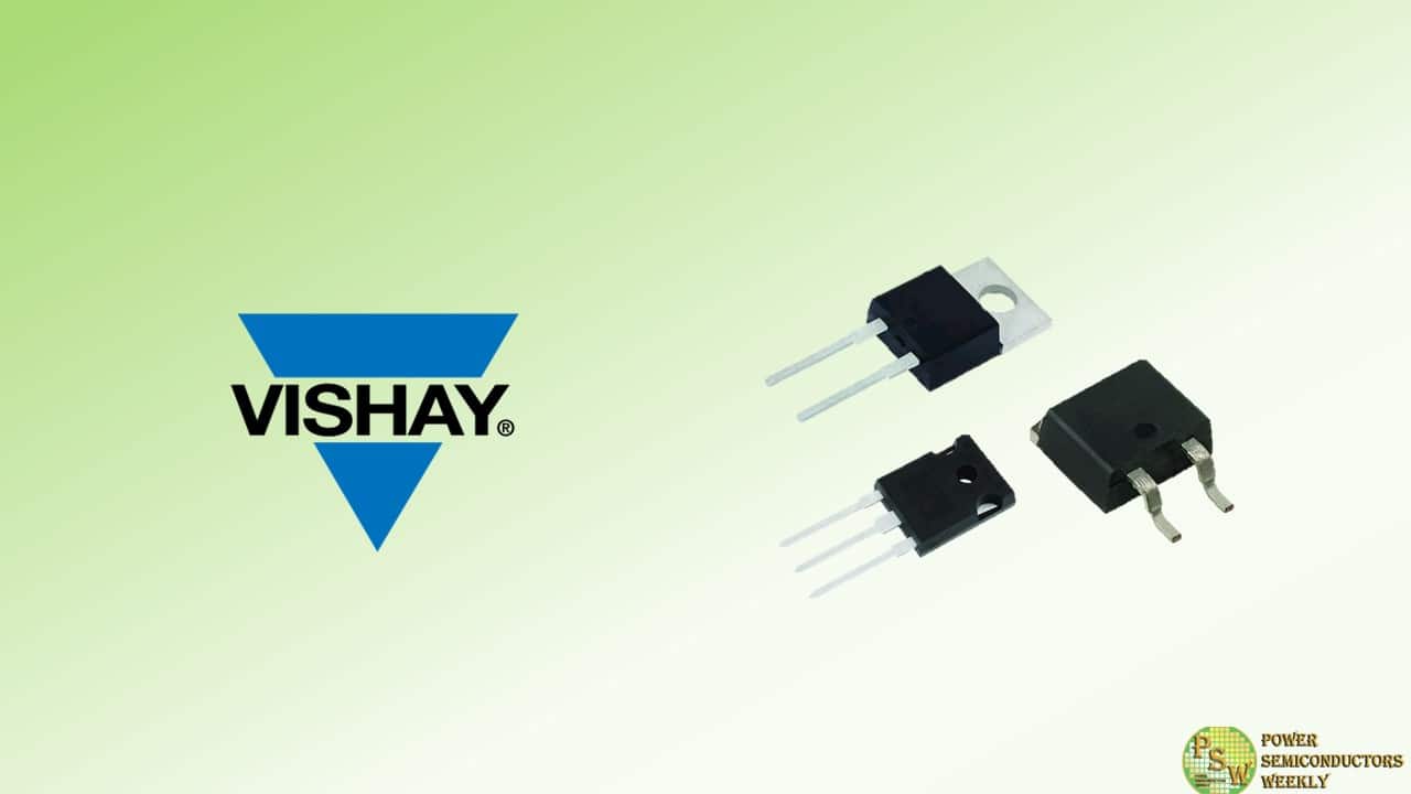
Vishay Intertechnology, Inc. introduced 16 new Gen 3 1200 V silicon carbide (SiC) Schottky diodes. Featuring a merged PIN Schottky (MPS) design, the Vishay Semiconductors devices combine high surge current robustness with low forward voltage drop, capacitive charge, and reverse leakage current to increase efficiency and reliability in switching power designs.
The next-generation SiC diodes released today consist of 5 A to 40 A devices in the TO-220AC 2L, TO-247AD 2L, and TO-247AD 3L through-hole and D2PAK 2L (TO-263AB 2L) surface-mount packages. The diodes offer a low capacitance charge down to 28 nC, while their MPS structure — which features a backside thinned via laser annealing technology — delivers a reduced forward voltage drop of 1.35 V. In addition, the devices’ low typical reverse leakage current down to 2.5 µA at 25 °C reduces conduction losses, ensuring high system efficiency during light loads and idling. Unlike ultrafast diodes, the Gen 3 devices have virtually no recovery tail, which further improves efficiency.
Typical applications for the diodes will include AC/DC PFC and DC/DC ultra high frequency output rectification in FBPS and LLC converters for solar power inverters; energy storage systems; industrial drives and tools; and datacenters. For the harsh environments of these applications, the devices combine operating temperatures to +175 °C with forward surge ratings to 260 A for high robustness. In addition, diodes in the D2PAK 2L package feature a molding compound with a high CTI ≥ 600, ensuring excellent electrical insultation at elevated voltages.
Offering high reliability, the RoHS-compliant and halogen-free devices have passed higher temperature reverse bias (HTRB) testing of 2000 hours and temperature cycling testing of 2000 thermal cycles.
Device Specification Table:
Part # IF(AV) (A) IFSM (A) VF at IF (V) QC (nC) Configuration Package VS-3C05ET12T-M3 5 42 1.35 28 Single TO-220AC 2L VS-3C10ET12T-M3 10 84 1.35 55 Single TO-220AC 2L VS-3C15ET12T-M3 15 110 1.35 81 Single TO-220AC 2L VS-3C20ET12T-M3 20 180 1.35 107 Single TO-220AC 2L VS-3C05ET12S2L-M3 5 42 1.35 28 Single D2PAK 2L VS-3C10ET12S2L-M3 10 84 1.35 55 Single D2PAK 2L VS-3C15ET12S2L-M3 15 110 1.35 81 Single D2PAK 2L VS-3C20ET12S2L-M3 20 180 1.35 107 Single D2PAK 2L VS-3C10EP12L-M3 10 84 1.35 55 Single TO-247AD 2L VS-3C15EP12L-M3 15 110 1.35 81 Single TO-247AD 2L VS-3C20EP12L-M3 20 180 1.35 107 Single TO-247AD 2L VS-3C30EP12L-M3 30 260 1.35 182 Single TO-247AD 2L VS-3C10CP12L-M3 2 x 5 42 1.35 28 Common cathode TO-247AD 3L VS-3C20CP12L-M3 2 x 10 84 1.35 55 Common cathode TO-247AD 3L VS-3C30CP12L-M3 2 x 15 110 1.35 81 Common cathode TO-247AD 3L VS-3C40CP12L-M3 2 x 20 180 1.35 107 Common cathode TO-247AD 3L Samples and production quantities of the new SiC diodes are available now, with lead times of 13 weeks.
Original – Vishay Intertechnology
-

Wolfspeed, Inc. provided an update on key milestones and an operational update.
Wolfspeed’s Mohawk Valley silicon carbide fab has reached 20% wafer start utilization, a critical step in the Company’s efforts to meet the growing demand for silicon carbide power devices. Additionally, Wolfspeed’s Building 10 Materials facility has achieved its 200mm wafer production target to support approximately 25% wafer start utilization at the Mohawk Valley fab by the end of calendar year 2024. Wolfspeed plans to update the market on its next utilization milestone for Mohawk Valley during its fiscal Q4 2024 earnings call in August.
The Mohawk Valley fab has also achieved LEED (Leadership in Energy and Environmental Design) Silver certification, a distinction from the world’s most widely used green building framework and rating system. The LEED Silver certification highlights Wolfspeed’s enduring commitment to going beyond compliance, promoting environmental health and industry leading sustainability.
This state-of-the-art Mohawk Valley facility is the world’s first purpose-built, fully automated 200mm silicon carbide fab, and when combined with Wolfspeed’s market-leading 200mm materials production, solidifies Wolfspeed’s competitive position as the only fully vertically integrated 200mm silicon carbide manufacturer at scale.
Additionally, Wolfspeed’s John Palmour Manufacturing Center (“the JP”) in Siler City, NC, which will be the world’s largest, most advanced silicon carbide materials facility upon completion, has installed and recently activated initial furnaces less than one year after vertical construction commenced. As a result, the facility is on schedule to achieve crystal qualification by early August 2024. This meaningful progress reinforces the Company’s confidence that it is well-positioned to ramp the JP in line with its target to deliver wafers from the facility to Mohawk Valley by the summer of 2025.
Wolfspeed also announced that it experienced an equipment incident at its Durham 150mm device fab that resulted in a temporary capacity reduction while the incident was being remediated. Production has been resumed and the Company expects that the Durham 150mm device fab’s capacity utilization can return to previously targeted levels by August. As a result of the production disruption, the Company does not expect an impact on fourth quarter revenue, but does expect to have an underutilization impact and incur other costs in the fourth quarter as described below.
“Having reached our 20% utilization target at Mohawk Valley, we are well-positioned to continue executing our 200mm vertical integration strategy ahead of other market participants,” said Gregg Lowe, president and CEO of Wolfspeed. “Further, recent advancements at the JP put Wolfspeed well on track to achieve our facility targets and significantly expand our materials capacity, driving meaningful progress towards our strategic goals. We quickly identified and resolved an equipment incident at our Durham 150mm device fab, and we continue to focus on execution as we move with urgency to continue this first-of-its-kind ramp.”
Business Outlook
Based on the Durham 150mm device fab equipment incident, Wolfspeed is updating its fiscal fourth quarter 2024 guidance as follows, and providing a preliminary outlook on fiscal first quarter 2025 revenue and non-GAAP gross margin:
- Targeted fiscal fourth quarter revenue from continuing operations is unchanged at $185 million to $215 million; and a potential negative impact to fiscal first quarter 2025 revenue of approximately $20 million.
- Targeted fourth quarter GAAP gross margins in the range of (4%) to 4% and non-GAAP gross margins in the range of 0% to 8%, due to an underutilization impact realized in the fourth quarter and other fourth quarter costs related to the equipment incident. The Company also expects fiscal first quarter 2025 non-GAAP gross margins in a similar range due to underutilization it will realize in the period.
- Fourth quarter GAAP net loss from continuing operations is targeted at $204 million to $182 million, or $1.61 to $1.44 per diluted share. Non-GAAP net loss from continuing operations is targeted to be in a range of $122 million to $105 million, or $0.96 to $0.83 per diluted share. Targeted non-GAAP net loss from continuing operations excludes $77 million to $82 million of estimated expenses, net of tax, primarily related to stock-based compensation expense, amortization of discount and debt issuance costs, net of capitalized interest, project, transformation and transaction costs and loss on Wafer Supply Agreement.
Original – Wolfspeed
-
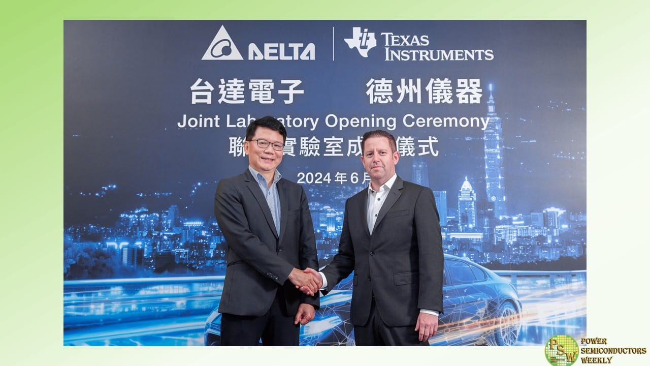
Texas Instruments announced a long-term collaboration with Delta Electronics, a global power and energy management manufacturer, to create next-generation electric vehicle (EV) onboard charging and power solutions. This work will leverage both companies’ research and development capabilities in power management and power delivery in a joint innovation laboratory in Pingzhen, Taiwan. Together, TI and Delta aim to optimize power density, performance and size to accelerate the realization of safer, faster-charging and more affordable EVs.
“The transition to electric vehicles is key to helping achieve a more sustainable future, and through years of collaboration with Delta Electronics, we have a solid foundation to build upon,” said Amichai Ron, senior vice president for Embedded Processing at TI. “Together with Delta, we will use TI semiconductors to develop EV power systems like onboard chargers and DC/DC converters that are smaller, more efficient and more reliable, increasing vehicle driving range and encouraging more widespread adoption of electric vehicles.”
“Delta has been developing high-efficiency automotive power products, systems and solutions since 2008 to help reduce transportation-related carbon emissions,” said James Tang, executive vice president of Mobility and head of the Electric Vehicle Solutions business group at Delta Electronics.
“Through the establishment of this joint innovation laboratory with TI, Delta intends to leverage TI’s abundant experience and advanced technology in digital control and GaN to enhance the power density and performance of our EV power systems. With more leading-edge product development and design capabilities, we aim to achieve closer technology exchange and collaboration to accelerate product development and improve product safety and quality. We look forward to furthering our technology leadership and creating a win-win situation in the rapidly developing electric vehicle market.”
Three phases of development for next-generation automotive power solutions
- Phase one for the collaboration focuses on Delta’s development of a lighter-weight, cost-effective 11kW onboard charger, using TI’s latest C2000™ real-time microcontrollers (MCUs) and TI’s proprietary active electromagnetic interference (EMI) filter products. The companies are working together using TI’s products to reduce the charger’s size by 30% while achieving up to 95% power conversion efficiency.
- In phase two, TI and Delta will leverage the latest C2000 real-time MCUs for automotive applications to enable automakers to achieve automotive safety integrity levels (ASILs) up to ASIL D, which represents the strictest automotive safety requirements. Highly integrated automotive isolated gate drivers will further enhance the power density of onboard chargers, while also minimizing overall solution size.
- In phase three, the two companies will collaborate to develop the next generation of automotive power solutions, capitalizing on TI’s more than 10 years of experience in developing and manufacturing products with gallium nitride (GaN) technology.
“The rapid growth of electronics in automotive applications has enabled more feature-rich, efficient and safer vehicles. However, technical challenges remain,” said Luke Lee, president of Taiwan, Japan, Korea and South Asia, Texas Instruments. “Having been in Taiwan for 55 years, coupled with decades of experience in automotive power management, TI has built a strong connection with the local automotive industry. Establishing this collaboration and joint innovation laboratory with Delta is just one more way TI is driving vehicle electrification forward.”
Original – Texas Instruments
-
Infineon Technologies AG introduced the new CoolGaN™ Transistor 700 V G4 product family. The devices are highly efficient for power conversion in the voltage range up to 700 V. In contrast to other GaN products on the market, the input and output figures-of-merit of these transistors provide a 20 percent better performance, resulting in increased efficiency, reduced power losses, and more cost-effective solutions. The combination of electrical characteristics and packaging ensures maximum performance in many applications such as consumer chargers and notebook adapters, data center power supplies, renewable energy inverters, and battery storage.
The product series comprises 13 devices with a voltage rating of 700 V and on-resistance range from 20 mΩ to 315 mΩ. The increased granularity in device specification, combined with a wide range of industry standard package options including PDFN, TOLL and TOLT allow R DS resistance and packages to be selected according to application requirements. As a result, both electrical and thermal system performance can be optimized and implemented in the most cost-effective solution.
The devices are characterized by a fast turn-on and turn-off speed and minimal switching losses. The on-resistance range enables power systems from 20 W to 25,000 W. In addition, the 700 V E-mode with the industry’s highest transient voltage of 850 V increases the reliability of the overall system as it offers greater robustness against anomalies in the user environment such as voltage peaks.
The CoolGaN Transistor 700 V G4 products in TOLL, PDFN 5×6 and 8×8 packages are available now, more variety in R DS(on) as well as the TOLT package will follow later this year.
Original – Infineon Technologies
-
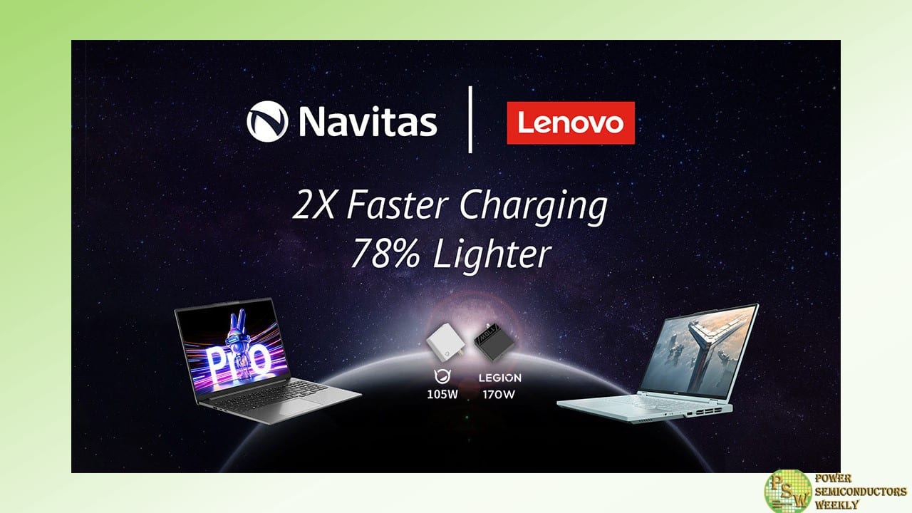
Navitas Semiconductor announced that its GaNFast power ICs have been selected to lead Lenovo’s latest GaN technology chargers; Xiaoxin 105 W GaN charger, and the Legion C 170 W GaN charger, respectively designed for daily travel and gaming power, bringing consumers a brand new fast charging experience.
The Xiaoxin 105 W GaN charger is designed for daily travel. It outputs 105 W of power and is equipped with 3 ports (2C1A) supporting multiple protocols; easily achieving the charging needs of various devices simultaneously. At only 206 g, the 105 W fast-charger is 41% lighter than a typical 100 W computer adapter and takes only 34 minutes to charge the Xiaoxin 16 Pro to 50%. The Navitas NV6138 GaNFast power IC with GaNSense™ technology is at the heart of the high-frequency flyback topology design, providing a stable, durable, and efficient charging experience.
The Legion C170 W GaN charger is designed specifically for hardcore gamers. It delivers 170 W of continuous power through a single port to meet the high-power demands of gaming devices. At only 245 grams, it’s 78% lighter than Legion Y9000P’s original inbox charger and can charge up to 2 times faster than the Legion C140 W Charger. The Navitas NV6136 GaNFast power IC with GaNSense technology is used in the PFC stage, featuring loss-less current sensing and 6 times faster short-circuit protection than competing solutions, delivering cooler operation, superior efficiency, reliability, and power density.
Lenovo’s long-term collaboration with Navitas has brought a series of groundbreaking fast chargers to the market and played a significant role in raising market awareness on showcasing the benefits of GaN technology. At the Lenovo YOGA CC65 dual-port GaN charger launch event in 2021, Navitas’ 6-inch GaN wafer and GaNFast power ICs were publicly showcased for the first time, unveiling the mysteries of this leading technology to consumers.
In terms of gaming products, Navitas collaborated with Lenovo to create a 90 W charger for the Lenovo Legion Pro Gaming Phone and a 135 W, C135 W GaN charger for the Legion 5 and 5 Pro Gen 7 laptops. For lightweight travel, Lenovo developed a series of compact, lightweight powerful GaN chargers using Navitas technology, including the revolutionary compact Thinkplus ‘lipstick’ and the ultra-thin Thinkbook ‘biscuit’ charger.
Lenovo and Navitas are not only partners in power technology but also pioneers in sustainability. Lenovo Group is verified by the Science Based Targets initiative (SBTi) for net zero targets and Navitas is the world’s first power semiconductor company to achieve CarbonNeutral® certification. Navitas’ advanced GaN technology enables Lenovo to continuously create smaller, lighter chargers with higher power density, significantly reducing the number of passive and magnetic components inside the charger, achieving CO2 reduction in production through “dematerialization”. The increased efficiency reduces power loss during use, thus further lowering carbon emissions in the product lifecycle.
“With the support of Navitas GaNFast power ICs, we have successfully introduced two new Xiaoxin and Legion GaN chargers to the market, enabling a lightweight and powerful charging experience for daily travel and gaming performance,” said Elon Chen, Product Manager of Consumer Business for Lenovo Group China. “Moreover, the successful application of Navitas’ GaNFast technology continuously reduces the size and weight of chargers, highly increasing efficiency, bringing convenience to consumers, while contributing to carbon reduction.”
“Powerland is very pleased to collaborate with Navitas again to create two high-performance and lightweight GaN chargers for Lenovo,” said Dr. Wang Chuanyun, VP of R&D for Powerland Group. “Powerland is dedicated to pushing the envelope of technology to build leading power products for our clients. Efficient, reliable, and easy-to-use GaNFast power ICs are crucial to realize that.”
“Navitas is very honored to enter Lenovo’s supply chain twice in a short period, providing high-efficiency and stable GaNFast fast charging power into two important Lenovo products,” said Charles Zha, VP and GM of Navitas China. “By working closely with Powerland, our highly integrated GaNFast technology has enabled Lenovo to continuously achieve leading-edge results in size, performance, and reliability of chargers. With innovative laptops like AI PCs on the rise, Navitas predicts a surge in demand for powerful GaNFast charging solutions. Navitas is on a mission to push the limits of gallium nitride technology, empowering global partners like Lenovo to slash energy usage and emissions in charger and adapter production. Together, we will speed towards a greener, more sustainable planet!”
Original – Navitas Semiconductor
-

Renesas Electronics Corporation announced that it has completed the acquisition of Transphorm, Inc. as of June 20, 2024. With the closing of the acquisition now completed, Renesas will immediately start offering GaN-based power products and related reference designs to meet the rising demand for wide bandgap (WBG) semiconductor products.
WBG materials such as GaN and silicon carbide (SiC) are considered key technologies for next-generation power semiconductors due to their superior power efficiency, higher switching frequencies and small footprints compared to conventional silicon-based devices. Both GaN and SiC-based products are expected to grow rapidly over the next decade, driven by demand from electric vehicles (EVs), inverters, data center servers, artificial intelligence (AI), renewable energy, industrial power conversion, consumer applications and others.
“Customers instantly benefit from the new GaN products through turnkey reference designs, which integrate technologies from both companies,” said Chris Allexandre, Senior Vice President and General Manager of Power at Renesas. “Adding GaN into our portfolio also reinforces our commitment to develop products and technology that make people’s lives easier. Providing robust and sustainable power solutions that save energy, reduce cost and minimize environmental impacts does just that.”
Investing in the power business is an important part of Renesas’ strategy for achieving sustainable, long-term growth. Other recent moves that Renesas has made to bolster this market segment include: the opening of the Kofu Factory, a dedicated 300-mm wafer fab for power products; ramping up a new SiC production line at the Takasaki Factory; and forging an agreement with Wolfspeed to secure a steady supply of SiC wafers over the next 10 years. With GaN technology now part of Renesas’ portfolio, Renesas is poised to offer more comprehensive power solutions to support the evolving needs of customers across a broad range of applications.
On the same day that it completed the acquisition of Transphorm, Renesas rolled out 15 new Winning Combinations, market-ready reference designs that combine the new GaN products with Renesas’ embedded processing, power, connectivity and analog portfolios. These include the designs of Transphorm’s automotive-grade GaN technology integrated for on-board battery chargers as well as 3-in-1 powertrain solutions for EVs.
Some examples are:
- 500W Onboard Battery Charger for 2-Wheeler EV
- 3-in-1 EV Unit: Inverter, Onboard Charger, DC/DC Converter
- 240W 48V Extended Power Range AC/DC Adapter
- 3.6KW Bi-directional Digital Power DAB System
Founded in 2007 in Goleta, California, Transphorm, with roots from the University of California at Santa Barbara and the Wide Bandgap industry, is built on a foundation of unique technology entrepreneurship. Transphorm, a leading innovator in GaN semiconductors designs, manufactures and sells high-performance and high-reliability GaN power products for a broad spectrum of high-voltage power conversion applications.
Original – Renesas Electronics
-

Electrification, renewables and artificial intelligence are global megatrends converging and driving unprecedented demands for advanced power semiconductors capable of optimizing energy conversion and management. In a strategic move toward addressing these demands, onsemi announced plans to establish a state-of-the-art, vertically integrated silicon carbide (SiC) manufacturing facility in the Czech Republic. The site would produce the company’s intelligent power semiconductors that are essential for improving the energy efficiency of applications in electric vehicles, renewable energy and AI data centers.
“Our brownfield investment would establish a Central European supply chain to better service our customers’ rapidly increasing demand for innovative technologies that improve the energy efficiency in their applications,” said Hassane El-Khoury, president and CEO, onsemi. “Through a close collaboration with the Czech government, the expansion would also enhance our production of intelligent power semiconductors that are essential to helping ensure the European Union is able to achieve its ambitions to significantly reduce carbon emissions and environmental impact.”
“onsemi’s decision to expand in Czechia is a clear confirmation of our country’s attractiveness for foreign investment and will bring significant momentum for the development of our economy,” said Mr. Jozef Síkela, Minister of Industry and Trade of the Czech Republic. “This investment not only strengthens our position in the semiconductor field but can also contribute to the development of the automotive industry and help us with its adaptation to the rise of electromobility.”
onsemi’s plan to expand SiC manufacturing with a multi-year brownfield investment of up to $2 billion (44 billion CZK) is part of the company’s previously disclosed long-term capital expenditure target. This investment would build on the company’s current operations in the Czech Republic, which include silicon crystal growth, silicon and silicon carbide wafer manufacturing (polished and EPI) and a silicon wafer fab. Today, the site can produce more than three million wafers annually, including more than one billion power devices. Upon completion, the operation would contribute annually more than $270 million USD (6 billion CZK) to the country’s GDP.
Pending all final regulatory and incentive approvals, including the investment incentive approval by the government of the Czech Republic and its notification to the European Commission, this would be one of the largest private sector investments in the Czech Republic’s history and would further contribute to the prosperity and economic dynamism of the Zlín region. onsemi is one of the first companies to invest in advanced semiconductor manufacturing in the Central European region.
With this investment, the company would contribute to the strategic positioning of the region within the EU’s semiconductor value chain and demonstrate that all EU countries can benefit from the European Chips Act. The announcement also reflects onsemi’s strategic alignment with the overarching goals of the European Chips Act of increasing market share and technological advancement to strengthen the resilience of the EU’s semiconductor supply chains in times of ever-growing demand.
Silicon carbide is a critical material for high-power, high-temperature applications, and is extremely difficult to produce. onsemi is one of the only companies in the world with the ability to manufacture SiC-based semiconductors from crystal growth to advanced packaging solutions. By expanding its production facilities in the Czech Republic, onsemi would be faster to provide supply assurance for customers, strengthening its leadership in intelligent power solutions. This integration would also enable onsemi to leverage its latest advancements in research and development (R&D) to maximize manufacturing and production efficiency.
Original – onsemi
