-

Infineon Technologies AG received the German Brand Award in the renowned “Best of Category” as “Excellent Brands – Corporate Brand of the Year”. The German Council of Design recognizes Infineon’s exceptional brand development, highlighting the company’s dedication to establishing a consistent brand that harmonizes seamlessly with its corporate strategy.
“To receive the German Brand Award as Corporate Brand of the Year is a special recognition for Infineon’s brand development over the past years,” said Andreas Urschitz, Member of the Management Board and Chief Marketing Officer of Infineon. “We are a global technology and thought leader with a clear vision and decisive actions. As a company, we are dedicated to driving decarbonization and digitalization through our solutions and in our business areas, together with our customers and partners. This commitment is deeply rooted in our corporate strategy, our brand, and within the entire global Infineon team.”
The award underlines Infineon’s commitment to excellence and innovation in brand strategy and design. It also reflects a strategic and decisive approach in the brand and corporate strategy, which ultimately enhances the company’s market presence with its audience.
The jury of the German Brand Award, which consists of members of the German Council of Design, acknowledged Infineon’s brand identity that resonates with its target audience while continuously staying true to its core values and vision.
The jury’s statement states: “Infineon has been a strong brand for 25 years – and also ‘Corporate Brand of the Year’ in 2024. The semiconductor manufacturer has decisively developed its strategy and design to link the brand even more closely with the corporate strategy. The close integration, including vision, mission and values, is exemplary and contributes to an outstanding positioning. Only a few companies in the competitive arena have such a consistent and distinctive brand. The dedicated 360-degree brand development and, above all, implementation is credible and has a high unique selling point.”
The German Brand Award is the award for successful brand management, initiated by Germany’s design and brand authority. Judged by a top-tier jury of experts from brand management and brand science, the German Brand Award discovers, presents and honors unique brands and brand makers.
Original – Infineon Technology
-
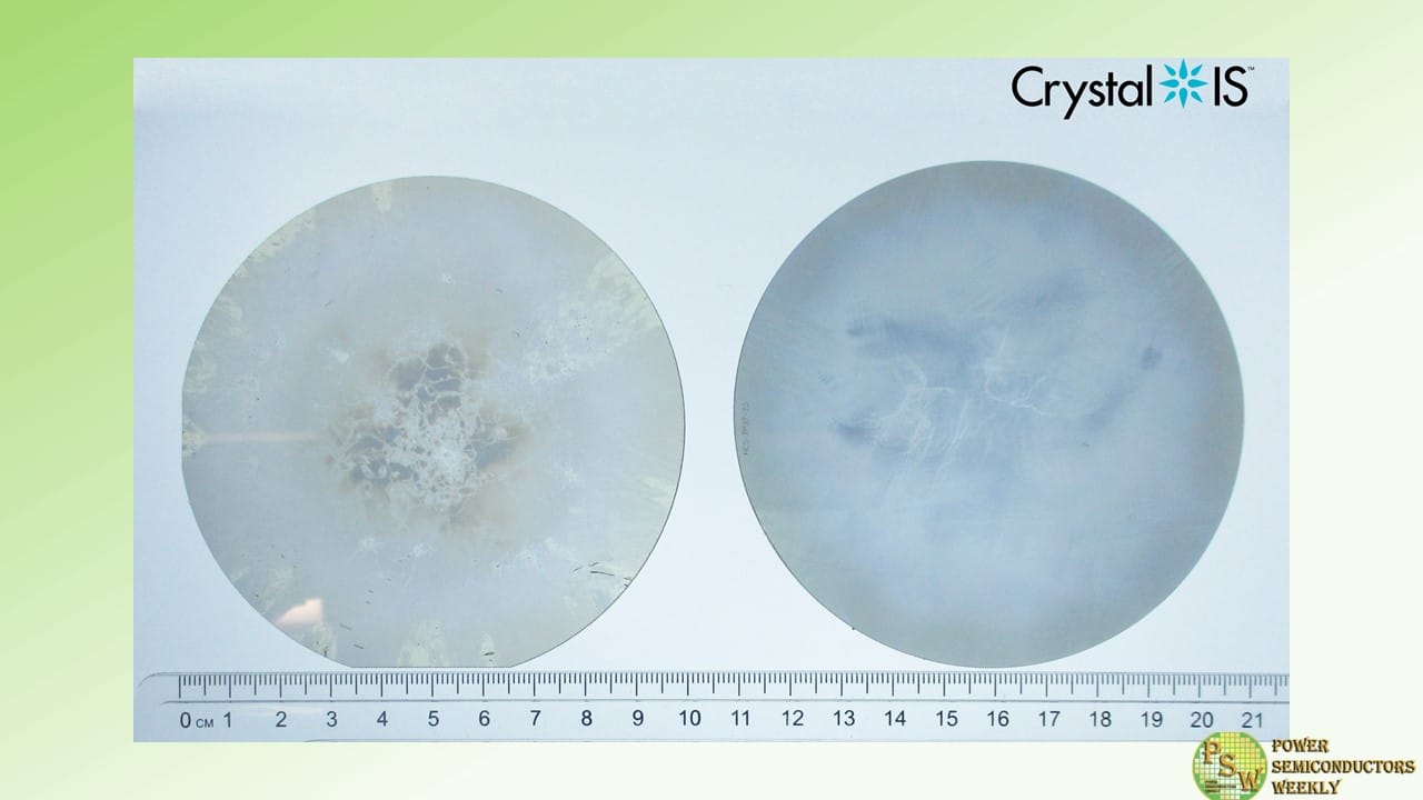
Crystal IS, an Asahi Kasei company, announced production of 100 mm diameter single-crystal aluminum nitride (AlN) substrates with 99% usable area, based on current requirements for UVC LEDs. This improved quality is steadily approaching that of Crystal IS’ existing 2-inch substrates used in the production of its UVC LEDs. The ultra-wide bandgap and high thermal conductivity of AlN helps improve device reliability and performance in both UVC LEDs and other next generation RF and power devices.
“The improvement of our large diameter substrate quality over the last nine months showcases the expertise of our team in aluminum nitride innovation,” said Eoin Connolly, President and CEO of Crystal IS. “The inherent benefits of aluminum nitride are unlocking new applications in RF and power devices—we are excited to work with our partners to further develop this material to meet their needs.”
This achievement follows the company’s announcement of the first ever recorded 100 mm diameter in August 2023, which won an excellence award at Semiconductor of the Year in electronic materials for the Semiconductors Category. The Semiconductor of the Year Awards are organized by Electronic Device Industry News, an industry journal published in Tokyo by SangyoTimes Inc.
Crystal IS manufactures bulk aluminum nitride substrates at its headquarters in Green Island, New York and began selling 2-inch diameter substrates for research and development in RF and power devices in late 2023. This 100 mm diameter milestone accelerates the development of new applications on aluminum nitride substrates as it integrates into existing fabrication lines for power and RF devices using alternative materials. The company plans to offer 100 mm diameter substrates manufactured in its US facility to key partners this year as they expand their focus beyond UVC LEDs.
Original – Crystal IS
-
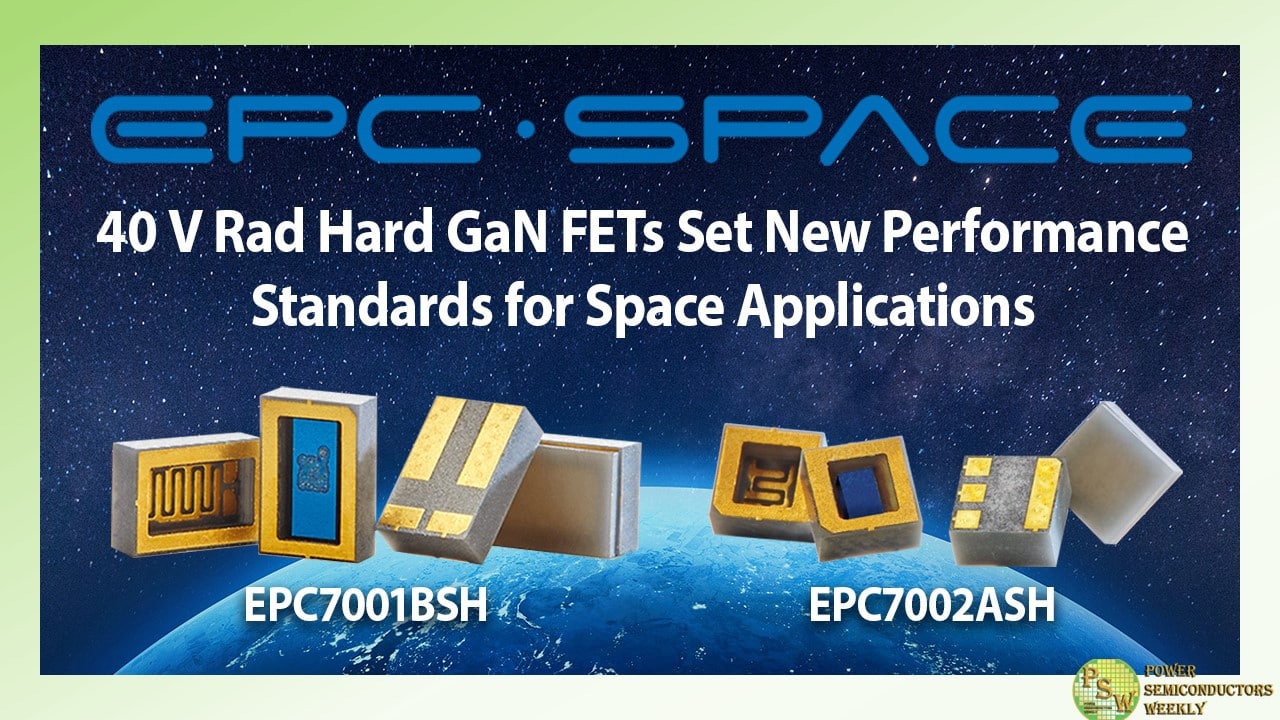
EPC Space announced the introduction of two new rad-hard GaN discretes with low on-resistance and extremely low gate charge for high power density solutions that are lower cost and more efficient than the nearest comparable radiation-hardened silicon MOSFET.
The EPC7001BSH is a Rad-Hard eGaN® 40 V, 50 A, 11 mΩ Surface Mount (FSMDB) and the EPC7002ASH is a Rad-Hard eGaN 40 V, 15 A, 28 mΩ Surface Mount (FSMDA). Both devices have a total dose radiation rating greater than 1,000K Rad(Si) and SEE immunity for LET of 83.7 MeV/mg/cm2 with VDS up to 100% of rated breakdown. These devices come packaged in hermetic packages in very small footprints.
EPC’s eGaN FETs and ICs offer a higher performing alternative to conventional rad hard silicon devices for high reliability and space applications. EPC’s Rad hard devices are significantly smaller, have 40 times better electrical performance, and lower overall cost than rad hard silicon devices. Moreover, EPC Space’s rad hard devices exhibit superior resistance to radiation, supporting higher total radiation levels and SEE LET levels compared to traditional silicon solutions.
Part Number Drain to Source Voltage (VDS) Drain to Source Resistance (RDS(on)) Single-Pulse Drain Current (IDM) Package Size (mm) Total Dose (TID) Heavy Ion Single Event Effects (SEE) EPC7001BSH 40 11 mΩ 120 5.7 x 3.9 1 Mrad SEE immunity up to LET of 83.7 MeV/mg/cm2 with VDS up to 100% of rated Breakdown EPC7002ASH 40 28 mΩ 40 3.4 x 3.4 1 Mrad SEE immunity up to LET of 83.7 MeV/mg/cm2 with VDS up to 100% of rated Breakdown With higher breakdown strength, lower gate charge, lower switching losses, better thermal conductivity, and lower on-resistance, power devices based on GaN significantly outperform silicon-based devices and enable higher switching frequencies resulting in higher power densities, higher efficiencies, and more compact and lighter weight circuitry for critical spaceborne missions.
Applications benefiting from the performance of these products include DC-DC power supplies for satellites and space mission equipment, motor drives for robotics, instrumentation and reaction wheels, deep space probes, and ion thrusters.
“These two new additions to our rad-hard product line offer designers high power and low on-resistance solutions enabling a generation of power conversion and motor drives in space operating at higher efficiencies, and greater power densities than what is achievable with traditional silicon-based rad-hard solutions,” said Bel Lazar, CEO of EPC Space.
Original – EPC Space
-
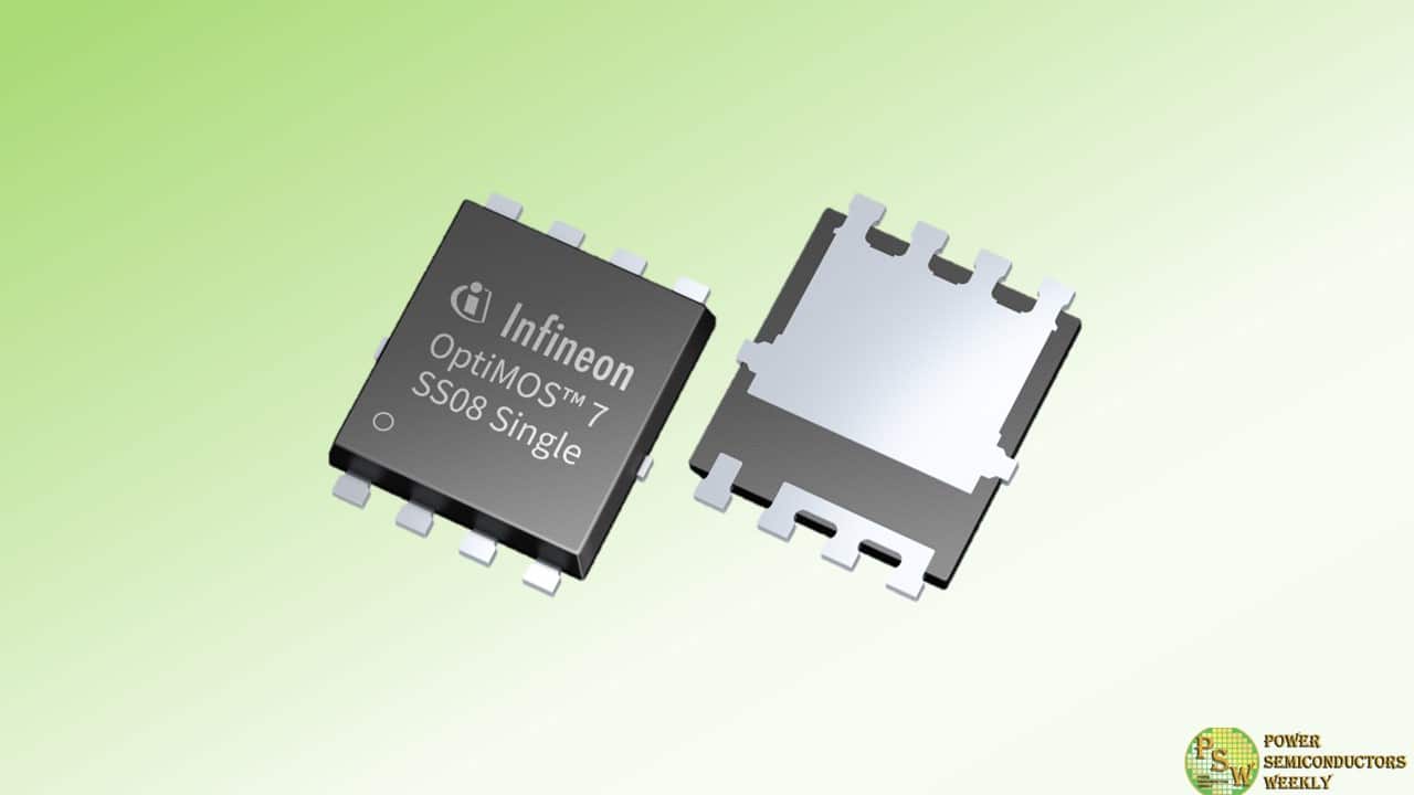
Infineon Technologies AG is expanding its portfolio of next-generation OptiMOS™ 7 MOSFETs for automotive applications: the portfolio of 40 V products now includes additional devices in robust, lead-free packages. In addition, 80 V and 100 V OptiMOS 7 MOSFETs are now also available.
The MOSFETs are optimized for all standard and future automotive 48 V applications, including electric power steering, braking systems, power switches in new zone architectures, battery management, e-fuse boxes, DC/DC, and BLDC drives in various 12 V and 48 V electrical system applications. They are also suitable for other transportation applications such as light electric vehicles (LEV), e2wheelers, eScooters, eMotorcycles, and commercial and agricultural vehicles (CAV).
“As a technology leader in power semiconductors, Infineon is committed to shape the future technology standards in automotive power MOSFETs in terms of power efficiency, innovative and robust power packaging with high quality,” said Axel Hahn, Senior Vice President and General Manager Automotive LV MOSFETs of Infineon. “We are providing our customers a diverse product portfolio and are addressing all their requirements to drive the development of modern automotive applications.”
By combining 300 mm thin-wafer technology and innovative packaging, the new OptiMOS 7 technology enables significant performance advantages in all available voltage classes. As a result, the components are now available in various rugged automotive power packages, including Single SSO8 (5×6), Dual SSO8 (5×6), mTOLG (8×8) and sTOLL (7×8).
The family offers high power density and energy efficiency with the industry’s lowest on-state resistance (e.g. 1.3 mΩ max in a single SSO8 (5×6) 80V package) in the smallest form factor. The devices also offer reduced switching losses, improved Safe Operating Area (SOA) robustness and high avalanche current capability. With this, they enable a highly efficient system design for tomorrow’s automotive applications.
Original – Infineon Technologies
-
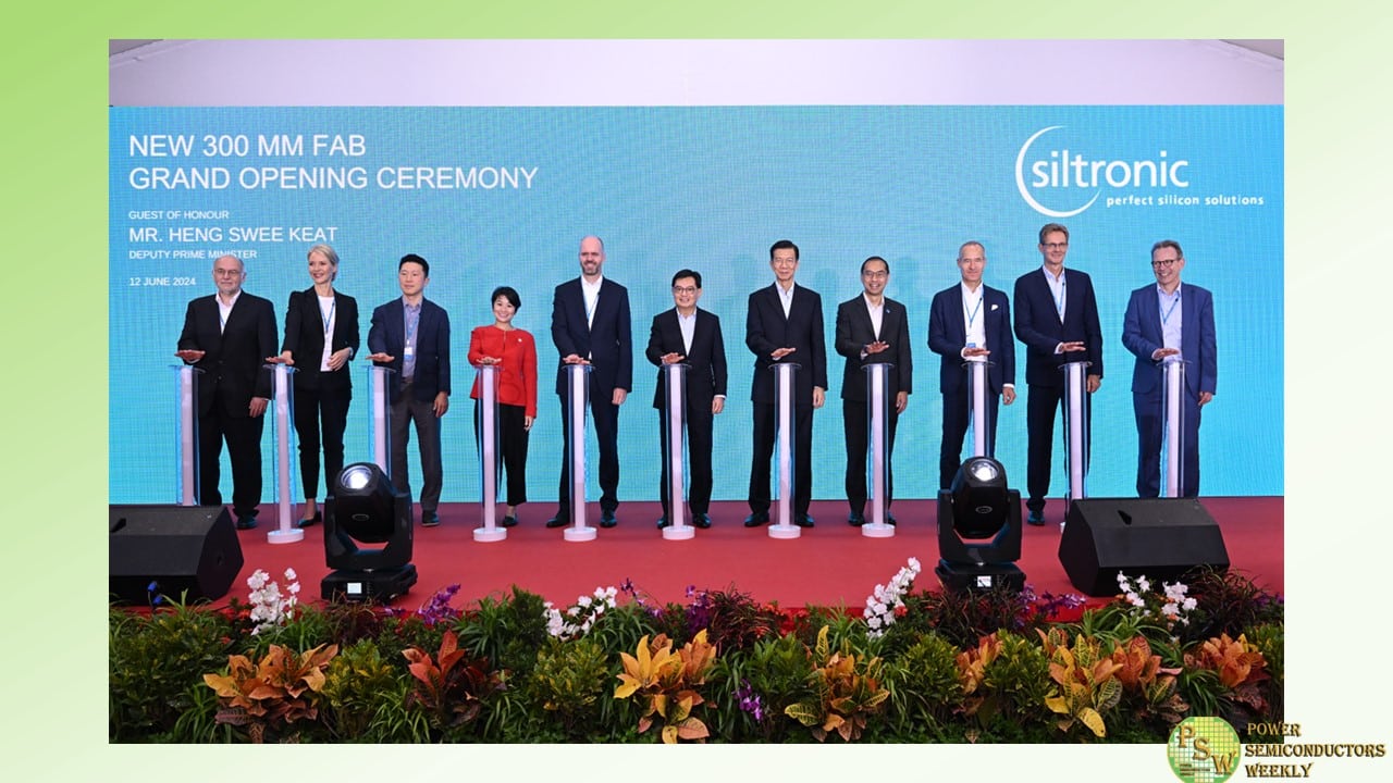
June 12 marked a milestone in the history of Siltronic AG: after more than 500 construction days and roughly 23 million working hours, Siltronic inaugurated one of the world’s most advanced wafer fabs. The inauguration of the new production facility, which is one of the most modern and cost-efficient of its kind, took place in Singapore.
The highly automated fab at JTC’s Tampines Wafer Fab Park was officially opened in the presence of around 150 guests, including numerous high-ranking representatives of the Singaporean government, customers and suppliers. Singapore’s Deputy Prime Minister Heng Swee Keat was the Guest of Honour to grace the occasion. The fab was commissioned at the beginning of 2024 and will now be ramped to full capacity over several years.
“With our new fab, we will accompany the future growth of the wafer industry for many years to come and take Siltronic to a new level. What the entire team, including all business partners, has achieved is a masterpiece, and I would like to thank everyone for their outstanding contribution,” said Dr. Michael Heckmeier, CEO of Siltronic AG, in his speech.
Ms. Jacqueline Poh, Managing Director of Singapore Economic Board (EDB) said: “We are proud of our long-standing partnership with Siltronic. As one of top 5 global wafer suppliers, Siltronic’s new fab is a significant expansion that not only supplies to Singapore’s semiconductor industry but also strengthens the resilience of the global semiconductor supply chain. This investment will create good jobs and further grow the existing collaboration that Siltronic has with local suppliers in automation and precision components.”
The success story of Siltronic in Singapore began in 1997 with the founding of Siltronic Singapore Pte. Ltd. in JTC’s Tampines Wafer Fab Park. The first 200 mm wafers were produced as early as 1999. This was followed in 2006 by the establishment of a joint venture with Samsung and the start of construction of the first 300 mm fab, from which the first wafers were delivered to customers in 2008. The foundation stone for the second 300 mm fab was laid in 2021, and it was officially opened today. Singapore is Siltronic’s largest production site.
Today’s inauguration of the state-of-the-art wafer fab in Singapore is not only the largest investment in Siltronic’s history, but also a milestone of which Siltronic is extremely proud. With its high level of automation and impressive efficiency, the fab sets new standards in our industry and strengthens Siltronic’s position as one of the world’s leading wafer manufacturers.
Original – Siltronic
