• onsemi Unveiled 800A 1200V QDual3 IGBT Power Module

    onsemi Unveiled 800A/1200V QDual3 IGBT Power Module

    3 Min Read

    The latest onsemi 7th generation 1200V QDual3 Insulated Gate Bipolar Transistor (IGBT) power modules offer increased power density and deliver up to 10% more output power than other available competing products. Based on the latest Field Stop 7 (FS7) IGBT technology, the 800-amp (A) QDual3 module delivers industry-leading efficiency to reduce system costs and simplify designs.

    In a 150KW inverter, the QDual3 module will dissipate 200 watts (W) less in losses compared to the closest competition, significantly reducing heatsink size. QDual3 is engineered to work under harsh conditions and is ideal for high-power electronics converters such as central inverters in solar farms, energy storage systems (ESS), commercial agricultural vehicles (CAVs) and industrial motor drives.

    Currently, two products are available depending on the applications – NXH800H120L7QDSG and SNXH800H120L7QDSG.

    Increasing renewable energy adoption amplifies the need for solutions that can manage peak demand and ensure continuous power supply. Peak shaving, the practice of reducing electricity use during peak hours, is essential for maintaining electric grid stability and reducing costs. Using the QDual3 modules, manufacturers can construct a solar inverter and ESS that output more power in the same system size, enabling more efficient energy management and storage capabilities, and allowing for a smoother integration of solar power into the grid.

    The modules also mitigate the intermittency of solar energy by storing excess power in an ESS, ensuring a reliable and consistent energy flow. For large systems, the modules can be paralleled to increase the output power up to a couple of MWs and compared to traditional 600 A module solutions, the 800 A QDual3 significantly reduces the module quantity, greatly simplifying design complexity and cutting system costs.

    The QDual3 IGBTs module features an 800 A half-bridge configuration that integrates the latest Gen7 trench Field Stop IGBT and diode technology using onsemi’s advanced packaging techniques to reduce switching and conduction losses.

    With FS7 technology, the die size is reduced by 30%, allowing more die per module, increasing the power density to enable the maximum current capacity up to 800 A or higher. With an IGBT Vce(sat) as low as 1.75V (175°C) and low Eoff, the 800 A QDual3 module dissipates 10% lower energy losses than the next-best alternative. The modules also meet the stringent standards required of an automotive application.

    “Increased electrification of commercial fleets such as trucks and busses and the need of renewable energy sources demand solutions that can generate, store and distribute power more efficiently. Transferring energy from renewable sources to the grid, storage systems and to downstream loads with the lowest power losses possible is increasingly critical,” said Sravan Vanaparthy, vice president, Industrial Power Division, Power Solutions Group, onsemi. “With its industry-standard pin-out and market-leading efficiencies, QDual3 enables power electronics designers to plug and play these modules for an immediate performance boost in their systems.”

    Original – onsemi

    Comments Off on onsemi Unveiled 800A/1200V QDual3 IGBT Power Module
  • Texas Instruments Introduced Industry's First 650V Three-Phase GaN IPM

    Texas Instruments Introduced Industry’s First 650V Three-Phase GaN IPM

    3 Min Read

    Texas Instruments introduced the industry’s first 650V three-phase GaN IPM for 250W motor drive applications. The new GaN IPM addresses many of the design and performance compromises engineers typically face when designing major home appliances and heating, ventilation and air-conditioning (HVAC) systems.

    The DRV7308 GaN IPM enables more than 99% inverter efficiency, optimized acoustic performance, reduced solution size and lower system costs. It is on display at the Power Electronics, Intelligent Motion, Renewable Energy and Energy Management (PCIM) Conference, held June 11-13 in Nuremberg, Germany.

    “Designers of high-voltage home appliances and HVAC systems are striving to meet higher energy-efficiency standards to support environmental sustainability goals around the world,” said Nicole Navinsky, Motor Drives business unit manager at TI. “They are also addressing consumer demand for systems that are reliable, quiet and compact. With TI’s new GaN IPM, engineers can design motor driver systems that deliver all of these expectations and operates at peak efficiency.”

    Improve system efficiency and reliability with TI GaN

    Worldwide efficiency standards for appliances and HVAC systems such as SEER, MEPS, Energy Star and Top Runner are becoming increasingly stringent. The DRV7308 helps engineers meet these standards, leveraging GaN technology to deliver more than 99% efficiency and improve thermal performance, with 50% reduced power losses compared to existing solutions.

    In addition, the DRV7308 achieves industry-low dead time and low propagation delay, both less than 200ns, enabling higher pulse-width modulation (PWM) switching frequencies that reduce audible noise and system vibration. These advantages plus the higher power efficiency and integrated features of the DRV7308 also reduce motor heating, which can improve reliability and extend the lifetime of the system.

    To learn more about the benefits of GaN technology, read the white paper, “How three-phase integrated GaN technology maximizes motor-drive performance.”

    Advanced integration and high power density reduce solution size and costs

    Supporting the trend of more compact home appliances, the DRV7308 helps engineers develop smaller motor drive systems. Enabled by GaN technology, the new IPM delivers high power density in a 12mm-by-12mm package, making it the industry’s smallest IPM for 150W to 250W motor-drive applications.

    Because of its high efficiency, the DRV7308 eliminates the need for an external heatsink, resulting in motor drive inverter printed circuit board (PCB) size reduction of up to 55% compared to competing IPM solutions. The integration of a current sense amplifier, protection features and inverter stage further reduces solution size and cost.

    To learn about designing more efficient, compact motor systems, see the GaN IPM page on TI.com.

    This high-efficiency, high-voltage GaN IPM is the latest example of TI innovations to help solve engineering challenges and transform motor designs.

    TI’s reliable high-voltage technology at PCIM 2024

    Visitors to PCIM can see new products and solutions from TI that are enabling the transition to a more sustainable future with reliable high-voltage technology in Hall 7, Booth 652. In addition to the DRV7308 GaN IPM, TI highlights at PCIM include:

    • Next-generation electric vehicle (EV) propulsion system: TI is demonstrating a new 800V, 750kW SiC-based scalable traction inverter system for EV six-phase motors, in collaboration with EMPEL Systems. The demonstration features high power density and efficiency using TI’s high-performance isolated gate drivers, isolated DC/DC power modules and Arm® Cortex®-R MCUs.
    • TI’s manager of high-voltage power systems applications, Sheng-Yang Yu, will speak on June 11 in the Markt & Technik panel discussion: “Will SiC ultimately Hold its Own against GaN?”
    • TI’s manager of renewable energy systems, Harald Parzhuber, will speak on June 12 in Bodo’s Power Systems panel discussion: “GaN Wide Bandgap Design, the Future of Power.”

    Original – Texas Instruments

    Comments Off on Texas Instruments Introduced Industry’s First 650V Three-Phase GaN IPM
  • hofer powertrain and ETH Zurich to Collaborate on a Multilevel GaN Traction Inverter

    hofer powertrain and ETH Zurich to Collaborate on a Multilevel GaN Traction Inverter

    3 Min Read

    hofer powertrain announced the commencement of a groundbreaking research project in collaboration with the Swiss Federal Institute of Technology in Zurich (ETH Zurich), focusing on the development of a state-of-the-art multilevel Gallium Nitride (GaN) traction inverter. Supported by a prestigious funding from INNOSUISSE, the Swiss Agency of Innovation Promotion, which advances science-based innovations in the interest of the economy and society in Switzerland. The next steps in this project will enable the pursuit of cutting-edge advancements in power electronics even further.

    The core objective of the project is to rapidly develop an advanced multilevel traction inverter integrating Gallium Nitride (GaN) switches. hofer powertrain has made significant strides in developing advanced multilevel power electronics utilizing Gallium Nitride (GaN) chip technology over the last four years, resulting in enhanced efficiency and power density compared to silicon-based systems.

    Their latest 800V GaN inverters have showcased remarkable performance in tests. The collaborative project with ETH Zurich builds on that experience to realize a revolutionary inverter solution, which aims to leverage a novel modulation scheme, operate at very high switching frequencies, and incorporate a wide array of additional pioneering features that the company has been working on in recent years.

    ETH has appointed a highly qualified PhD candidate to lead the research efforts, ensuring the project benefits from fresh, innovative thinking and rigorous academic oversight. The project will be supervised by Professor Johann Biela from ETH Zurich, a renowned expert in power electronics, and Lukasz Roslaniec, the division lead of power electronics at hofer powertrain, who brings extensive industry experience to the table and has been working on these technologies proactively.

    The funding from Innosuisse underscores the project’s significance and potential impact in the country and the DACH-region. This financial support will facilitate the design of a new, optimized, and highly efficient three-level GaN power inverter, featuring adaptive gate drivers to improve switching controllability and further reduce energy losses. The outcome will significantly enhance the performance and efficiency of powertrain systems for modern electrified vehicles, making a substantial contribution to the future of mobility.

    Dr. Lukasz Roslaniec highlights the driving force behind this project, stating, “We eagerly anticipate the fruitful collaboration with ETH, renowned for its groundbreaking work in Power Electronics and Electric Drives. We are confident that our partnership will yield solutions that are not only technologically advanced and unparalleled but also financially accessible, thereby pushing the adoption of electric vehicles and environmental sustainability in the region and beyond.”

    Original – hofer powertrain

    Comments Off on hofer powertrain and ETH Zurich to Collaborate on a Multilevel GaN Traction Inverter
  • Infineon Technologies Pioneering in Semiconductor Industry with Comprehensive Product Carbon Footprint Data

    Infineon Technologies Pioneering in Semiconductor Industry with Comprehensive Product Carbon Footprint Data

    3 Min Read

    Infineon Technologies AG will provide customers with comprehensive Product Carbon Footprint (PCF) data, taking a pioneering role in the semiconductor industry. The company is committed to eventually providing PCF data for its entire product portfolio, starting now with about half of its portfolio.

    The initiative will empower customers to advance their own sustainability goals and reduce their carbon footprint effectively along the entire supply chain. The Product Carbon Footprint is a metric that quantifies the greenhouse gas emissions associated with an individual product, allowing the comparison of different products’ climate impact. Infineon will share more insights with customers at the upcoming PCIM trade fair in Nuremberg, Germany, from 11 to 13 June 2024.  

    “By providing comprehensive Product Carbon Footprint data, we are driving the vision of a net-zero society and empowering our customers to reduce carbon emissions even more effectively,” says Elke Reichart, Member of the Management Board and Chief Digital and Sustainability Officer at Infineon. “Infineon is taking a leading role in carbon transparency by committing to include the entire product portfolio over the coming years. This underlines our ambition to be a leader not only in terms of technology, but also sustainability.”

    The specific data Infineon provides on its individual products is essential for the growing number of customers who want to increase transparency on their own carbon footprint. Moreover, it supports informed decision making to leverage additional potential for reducing emissions along the value chain.

    In the absence of established industry standards, Infineon has developed a robust methodology to calculate the Product Carbon Footprint, incorporating customer needs and best practices. Infineon includes emissions from raw materials and supplies, its own manufacturing processes, manufacturing partners and transportation to the customer (“from cradle to gate”).

    This means that the Product Carbon Footprint reported by Infineon covers scope 1 and 2 emissions as well as scope 3 emissions from suppliers and manufacturing partners, all the way to the customer’s gate. The Product Carbon Footprint is expressed in kilograms of carbon dioxide equivalent (kg CO 2e).

    Infineon has published the assessment of reference product families on the Infineon website.

    Driving transparency goes hand in hand with Infineon’s strong commitment to decarbonization and digitalization. Infineon’s products make a major contribution to the global energy transition and thus to a net-zero society. They are used in solar and wind power plants, electric cars and increase energy efficiency in numerous applications, including AI data centers. Over their lifetime, the company’s chips overall save 34 times the amount of CO 2e emitted during their production.

    Breaking the carbon footprint down to the product level is another major milestone in Infineon’s sustainability journey. Infineon has already pledged to achieve carbon neutrality by 2030 for direct and indirect emissions (scope 1 and 2). Last year, the company additionally committed to setting a science-based target encompassing supply chain emissions (scope 3) as well.

    Original – Infineon Technologies

    Comments Off on Infineon Technologies Pioneering in Semiconductor Industry with Comprehensive Product Carbon Footprint Data
  • At PCIM Europe 2024, Fraunhofer IISB, Fraunhofer ISIT and Fraunhofer IMS to Present Entire Value Chain for Next-Gen Power Electronics

    At PCIM Europe 2024, Fraunhofer IISB, Fraunhofer ISIT and Fraunhofer IMS to Present Entire Value Chain for Next-Gen Power Electronics

    10 Min Read

    Wide-bandgap (WBG) semiconductor technology and artificial intelligence together are revolutionizing power electronics. A new class of intelligent power electronic systems is unlocking new performance and application areas. The high demands of system development impact the entire power electronics value chain. Specifically, this applies to semiconductor materials and devices as well as packaging and module technology. Extreme operating and environmental conditions demand maximum reliability and ultra-high performance. At PCIM Europe 2024, Fraunhofer IISB, Fraunhofer ISIT and Fraunhofer IMS together present the entire value chain for next-generation power electronics.

    All-electric Society
    In power electronics, a fundamental change is happening. Two very dynamic sectors are currently automotive electronics and energy technology. In both application areas, there is a race for ever more efficient, high-performance and cost-effective power electronics systems. On top of this, there are increased requirements in terms of the reliability and service life of the electronic parts and components.

    The main purpose of power electronics is the conversion and distribution of electrical energy using electronic switches between different sources, energy storages and loads that are electrically linked to each other. Power electronics fulfill these functions both in stationary applications, such as integrating renewable energy sources into the power grid, and more and more in mobile applications, like in battery electric vehicles. The central and crucial components here are the electrical converters, which can be used, for example, as chargers, voltage converters or drive inverters.

    Faster – Stronger – Higher
    With drive outputs of up to 1000 kW and ranges of over 1000 km, electric powertrains for electric cars have reached a new level. The electric converters are operating in the megawatt class. As a result, vehicle electronics are advancing vehemently into the area of larger drives and opening up further interesting fields of application. Outstanding examples are the emerging electrification in ships and aviation.

    Hybridization, i.e., the combination of combustion engines or jet propulsion systems with fuel cell technology and battery storage, promises enormous savings in terms of fuel consumption and emissions. Alongside batteries, hydrogen is becoming an interesting energy carrier. The hydrogen technology in turn opens up its own technological possibilities, such as the design of cryogenic converters or the use of superconducting cables and motor windings. However, classic silicon components have reached their physical limits and the use of wide-bandgap semiconductors such as silicon carbide or gallium nitride is a necessity.

    Taking off with WBG
    WBG-based power devices offer low on-state losses, enable higher switching frequencies and can handle high currents at high operating voltages. They provide superior thermal properties and are suitable for operation in a wide temperature range. Customized device and process technologies, such as VDMOS, pave the way to fully exploit the potential of WBG semiconductors for power electronics.

    In terms of industrial application, SiC (silicon carbide) and GaN (gallium nitride) semiconductor technologies have gained significant impact on the market. However, there are still unlocked advantages at system level in terms of cost, efficiency, and construction volume. Current research activities are focused on an in-depth understanding of device characteristics and materials properties, not only on device level.

    In the development of WBG-capable modules, especially GaN and SiC power modules, various technical challenges remain to be investigated. So, to realize highest efficiency power electronic conversion with fast switching, parasitic effects have to be minimized. In this context, the spatial and functional integra-tion of the semiconductor switches with the driver control is crucial.

    New challenges for WBG power modules come from extreme temperatures like cryogenic as well as high-temperature applications with appropriate adaptations to the packaging technology. Accordingly extended qualification measures and test procedures are required, that take novel failure mechanism into account. With special environmental and operational conditions, aviation is one of the hardest areas to conquer. Reliability is the key here, as failure rates must be precicely identified and extremely low. And all this with an outstanding power-to-weight ratio.

    Power Meets Intelligence
    Another trend in system development is apparent: the progressive integration of information and commu-nication technology.

    On-board power grids for aircrafts and vessels are comparable with the local power grid of a small town in terms of their complexity and dimensions. The grids connect many distributed sources and loads via long cables and transfer high power simultaneously. As a result, the focus is shifting to grid stability and droop control, i.e., the control and synchronization of generators and converters. Additional functions for monitoring, management and communication, as well as intelligent capabilites need to be implemented in the grids: On-board grids are evolving into smart grids. In stationary grid technology, especially in smart grids or local DC grids, as well as in battery systems for battery management, this transformation has been visible for a while now.

    The fusion with data processing requires an increasing integration of digital technology components. Microcontrollers and system on chips have long been used in drivers and control circuits for electronic power switches. Approaches from classic signal processing are also being applied, e.g., for forming the alternating current waveform to save space and material-intensive passive filter components. This is also exemplified by modular multi-level converters, which consist of a large number of freely configurable inverter cells and can be used to cover a very wide range of applications and performance.

    The Perfect Match
    A new class of intelligent power electronics with additional AI functionality, the so-called cognitive power electronics, is currently being developed further. These “perceptive systems” are equipped with sensors to detect various physical parameters and embedded electronics to record and analyze data in real time. Electric drives thereby become integrated intelligent systems that know about their present operating status. Based on methods of machine learning, cognitive power electronic systems can make predictions and react autonomously to internal and external influences and events.

    The high demands imposed by system developers affect all stages of the power electronics value chain. It is already apparent today that the demanded performance characteristics of the new type of power electronics can no longer be achieved with the existing semiconductor devices and system features. Power semiconductors based on ultra-wide bandgap materials and other innovative devices, such as integrated snubbers or active circuit breakers, are in the pipeline. Accompanying, the transition towards an all-electric society pushes the power electronic systems development to new performance levels.

    The integrated power electronic system – the symbiosis of innovative power semiconductor technologies, microelectronics and artificial intelligence – is becoming a reality.

    PCIM Europe 2024 Nuremberg – Excelling in Power Electronics

    At this year’s leading trade fair for power electronics in Europe – PCIM Europe 2024 in Nuremberg – three Fraunhofer Institutes are teaming up at their joint booth no. 6-368. From June 11 to 13, 2024, the Fraunhofer IISB, Fraunhofer ISIT and Fraunhofer IMS together present the entire value chain for next-generation power electronics.

    Visitors can expect exhibits on topics ranging from wide-bandgap and ultra-wide-bandgap semiconductors, (U)WBG-ready packaging and module technology, cryogenic to high-temperature, integrated passives, active fuse components, advanced sensor technology, MEMS integration, ultra-compact power converters and modular multi-level converters to electric powertrains for large-scale drives.

    PowerCare – Cognitive Power Electronics with Integrated Failure Protection
    The centerpiece of the joint booth and overlap of the expertise of the three partner institutes is the exhibition area for project PowerCare. PowerCare uses a new monitoring concept in the form of a miniaturized motor controller with integrated real-time failure prediction (edge AI) to detect upcoming maintenance needs in advance. This is laying the foundation for a new evolutionary stage of intelligent power modules. Simultaneously, the switch to vertical GaN MOSFETs allows for unrivaled power densities and ruggedness.

    Within the project, Fraunhofer ISIT works on novel, vertical GaN trench MOSFETs and their behavioral models. Fraunhofer IMS contributes embedded AI models integrated in a PWM controller for failure prediction of electric motors and GaN power semiconductors. Fraunhofer IISB demonstrates GaN MOSFETs and an in-telligent motor control with AI-based condition monitoring of the electric drive. For a market-oriented development of cognitive power electronics, the project partners Siemens AG, X-FAB Dresden GmbH & Co. KG, NXP® Semiconductors Germany GmbH, and TU Dortmund University provide support and valuable practical feedback.

    Fraunhofer Institute for Integrated Systems and Device Technology IISB
    The Fraunhofer IISB in Erlangen specializes in wide-bandgap semiconductors and efficient power electronics. Here, materials and device know-how merges with complex system development, especially for e-mobility and sustainable energy supply. With its solutions, the institute has been setting benchmarks in energy efficiency and power density, even for extreme operating conditions like in aviation and space.

    At its long-time no. 1 trade fair, the IISB shows the broad spectrum of its activities in high-performance power electronics. Starting from WBG and UWBG base materials over semiconductor technology with SiC device development and prototype processing, the spectrum ranges to hybrid integration, packaging and module technology. In the area of system integration, visitors await exciting exhibits showcasing medium voltage electronics and advanced SiC and GaN power electronics for automotive, maritime and aircraft applications. Special highlights are a fully integrated aircraft power train in the megawatt class and a crewless electric vertical take-off and landing vehicle for early AI-based forest fire detection.

    Fraunhofer Institute for Silicon Technology ISIT
    The Fraunhofer ISIT in Itzehoe is one of Europe’s most modern research facilities for microsystems technology and power electronics. At the heart of the institute are its cleanroom facilities, large enough not only to conduct research but also to manufacture the microchips developed on an industrial scale.

    At PCIM 2024, Fraunhofer ISIT gives insights into current and future activities in the areas power electronics and electronic energy systems. As a part of Fraunhofer’s GaN pilot line, an emerging, independent ecosystem for development activities ranging from epitaxy via device processing to application, the ISIT presents lateral and vertical GaN devices and its processing capabilities as well as GaN-on-QST services.

    With the concept Active Reliability, the institute shows condition monitoring techniques and data processing approaches such as data-fusion and digital twin for online state-of-health estimation, lifetime extension, and fault tolerance. Further highlights are the EnergyHub, a DC power router for multi-source integration and high-availability power supply and GaN-based converters for high-efficiency and high-density energy conversion.

    Fraunhofer Institute for Microelectronic Circuits and Systems IMS
    The Fraunhofer IMS in Duisburg is a trusted research and development partner for industry. Its goal is to develop customized sensor systems for specific needs in the areas of biomedical sensors, optical systems, open-source semiconductors, embedded AI, technology services and even quantum technology.

    At PCIM Europe 2024, Fraunhofer IMS presents innovative technologies in power electronics and RFID technology. The institute also offers solutions in ASIC and chip design as well as CMOS, MEMS and LiDAR. Its RISC-V processors deliver outstanding performance and improve efficiency and reliability in various applications. With the PredictiveBoX developed at the IMS, AI-based vibration analysis can be carried out and production optimized. In addition, customized vertical GaN switches enable savings of megatons of CO2.

    Research Fab Microelectronics Germany
    The overall framework is the Research Fab Microelectronics Germany FMD (acronym in German), a cooperation of the Fraunhofer Group for Microelectronics with the Leibniz institutes FBH and IHP. With more than 4,600 employees and a diversity of expertise and infrastructure, the virtual umbrella organization of FMD is the largest association of its kind in Europe. As a pioneer in cross-location and cross-technology cooperation, FMD is actively addressing the current and future challenges of electronics research to ensure the preservation and expansion of Germany’s and Europe’s technological sovereignty.

    Original – Fraunhofer IISB

    Comments Off on At PCIM Europe 2024, Fraunhofer IISB, Fraunhofer ISIT and Fraunhofer IMS to Present Entire Value Chain for Next-Gen Power Electronics
  • Mitsubishi Electric Added Two New SBD-embedded SiC-MOSFET Power Modules

    Mitsubishi Electric Added Two New SBD-embedded SiC-MOSFET Power Modules

    1 Min Read

    Mitsubishi Electric Corporation has begun shipping low-current 3.3kV/400A and 3.3kV/200A versions of a Schottky barrier diode (SBD) embedded silicon carbide (SiC) metal-oxide-semiconductor field-effect transistor (MOSFET) module for large industrial equipment, including rolling stock and electric power systems, from today, June 10.

    Together with the existing 3.3kV/800A version, the newly named UnifullTM series comprises three modules to meet the growing demand for inverters capable of increasing power output and power conversion efficiency in large industrial equipment. The new modules will be exhibited at major trade shows, including Power Conversion Intelligent Motion (PCIM) Europe 2024 in Nuremberg, Germany from June 11 to 13.

    Mitsubishi Electric’s SBD-embedded SiC-MOSFET modules, including the 3.3kV/800A version released on March 29, feature an optimized package structure to reduce switching loss and improve SiC performance. Compared to existing power modules, UnifullTM modules, significantly reduce switching loss and contribute to higher power output and efficiency in large industrial equipment, making them suitable for auxiliary power supplies in railcars and drive systems with relatively small capacities.

    Original – Mitsubishi Electric

    Comments Off on Mitsubishi Electric Added Two New SBD-embedded SiC-MOSFET Power Modules
  • Vishay Intertechnology to Bring Its First SiC MOSFETs to PCIM Europe 2024

    Vishay Intertechnology to Bring Its First SiC MOSFETs to PCIM Europe 2024

    3 Min Read

    Vishay Intertechnology, Inc. announced that at PCIM Europe 2024 the company will be showcasing its broad portfolio of power management solutions that address several increasingly important trends in power electronics, including e-mobility, high efficiency power conversion, energy storage, and grid management. In Hall 9, Booth 208, Vishay experts will be available to discuss the company’s extensive offering of passive and semiconductor solutions for these next-generation applications.

    Taking center stage for Vishay at PCIM will be the company’s newly released 1200 V MaxSiC™ series silicon carbide (SiC) MOSFETs, which deliver on-resistances of 55 mW, 95 mW, and 280 mΩ in standard packages for industrial applications, with custom products also available.

    In addition, Vishay will provide a roadmap for 650 V to 1700 V SiC MOSFETs with on-resistances ranging from 10 mΩ to 1 Ω. Vishay’s SiC platform is based on  proprietary MOSFET technology — enabled through the company’s  acquisition of MaxPower Semiconductor, Inc. — which will address market demands in traction inverter, photovoltaic energy conversion and storage, on-board charger, and charging station applications. At the booth, Vishay’s experts will also be discussing upcoming planned releases of the MaxSiC platform, including AEC-Q101 Automotive Grade products.

    At PCIM, Vishay will be offering a variety of application-focused demonstrations, including:

    • A high voltage intelligent battery shunt for 400 V and 800 V batteries
    • A 40 kW resettable electronic fuse (eFuse) for 400 V and 800 V battery electric vehicles (BEV)
    • A unidirectional, 11 kW three-phase AC on-board charger (OBC) with a BOM consisting of 90 % Vishay parts
    • A bidirectional 10 kW eFuse for 48 V applicationsA collaborative robot workstation featuring Vishay power resistors, ESTA power electronic capacitors (PEC), Automotive Grade diodes, SiC MOSFETs, and an SiC-based auxiliary power converter.

    Vishay passive components on display at PCIM will include IHPT series solenoid-based haptic actuators featuring Immersion Corporation licenses, a 5.5 kW transformer / inductor for LLC applications, and IHLE® series low profile, high current inductors with integrated e-field shields; wirewound resistors and charging resistors featuring hybrid wirewound technology; thick film power resistors; robust metallized polypropylene film capacitors, including AC and pulse capacitors and DC-Link capacitors with high temperature operation up to +125 °C and the ability to withstand temperature humidity bias (THB) testing of 85 °C / 85 % for 1000 h; X1, X2, and Y2 EMI suppression film capacitors certified to safety and humidity robustness grade IIIB; and DC and AC power electronic capacitors (PEC) with high impulse current ratings, low inductance, and high reliability.

    Highlighted Vishay semiconductor solutions will consist of surface-mount diodes in the eSMP® and FlatPAK 5×6 packages; leadless surface-mount diodes in the DFN, CLP, and LLP series packages; and 650 V and 1200 V SiC Schottky diodes up to 20 A in eSMP® series and 40 A in power packages for AC/DC power factor correction (PFC) and ultra high frequency output rectification. In addition, Vishay will be showcasing microBUCK® and microBRICK® buck regulators, including the 60 V input SiC967 synchronous buck regulator with integrated power MOSFETs and inductors; high voltage MOSFETs in the PowerPAK 10×12 package; automotive power modules in the EMIPAK 1B, MaacPAK, FlatPAK, and HC0 packages; and industrial power modules in Gen III TO-244, IAP, SOT-227, and MTC packages.

    Prior to the exhibition, on June 9, Vishay’s Sanjay Havanur — senior manager of system applications — will be presenting the seminar “Silicon Is Still Here: A Refresher on the Narrow Bandgap Power MOSFETs and Their Datasheets” at 2 p.m. in the Arvena Park Hotel. During the show, Claudio Damilano — director of product marketing and market development, power modules — will present “Evolution in Vishay Power Modules for E-Mobility: Solutions for High Voltage and Low Voltage Applications” on June 11, at 3:50 p.m. in Hall 6, Booth 220.

    Original – Vishay Intertechnology

    Comments Off on Vishay Intertechnology to Bring Its First SiC MOSFETs to PCIM Europe 2024
  • Microchip Technology Introduced an On-Board Charger Solution Based on mSiC™ MOSFETs

    Microchip Technology Introduced an On-Board Charger Solution Based on mSiC™ MOSFETs

    3 Min Read

    The market for Battery Electric Vehicles (BEVs) and Plug-in Hybrid Electric Vehicles (PHEVs) continues to grow as the push towards decarbonization requires sustainable solutions to reduce emissions. A critical application for EVs is the on-board charger, which converts AC power into DC power to recharge the vehicle’s high-voltage battery.

    Microchip Technology announced an On-Board Charger (OBC) solution that uses a selection of its automotive-qualified digital, analog, connectivity and power devices, including the dsPIC33C Digital Signal Controller (DSC), the MCP14C1 isolated SiC gate driver and mSiC™ MOSFETs in an industry-standard D2PAK-7L XL package.

    This solution is designed to increase an OBC system’s efficiency and reliability by leveraging the dsPIC33 DSC’s advanced control functions, the MCP14C1 gate driver’s high-voltage reinforced isolation with robust noise immunity and the mSiC MOSFETs’ reduced switching losses and improved thermal management capabilities. To further simplify the supply chain for customers, Microchip provides the key technologies that support the other functions of an OBC, including communication interfaces, security, sensors, memory and timing.

    To accelerate system development and testing, Microchip offers a flexible programmable solution with ready-to-use software modules for Power Factor Correction (PFC), DC-DC conversion, communication and diagnostic algorithms. The software modules in the dsPIC33 DSC are designed to optimize performance, efficiency and reliability, while offering flexibility for customization and adaptation to specific OEM requirements.

    “Microchip established an E-Mobility megatrend team with dedicated resources to support this growing market, so in addition to providing the control, gate drive and power stage for an OBC, we can also provide customers with connectivity, timing, sensors, memory and security solutions,” said Joe Thomsen, corporate vice president of Microchip’s digital signal controller business unit. “As a leading supplier to OEMs and Tier-1s, Microchip offers comprehensive solutions to streamline the development process, including automotive-qualified products, reference designs, software and global technical support.”

    Here is an overview of the key components in this OBC solution:

    • The dsPIC33C DSC is AEC-Q100 qualified and features a high-performance DSP core, high-resolution Pulse-Width Modulation (PWM) modules and high-speed Analog-to-Digital Converters (ADCs), making it optimal for power conversion applications. It is functional safety ready and supports the AUTOSAR® ecosystem.
    • The MCP14C1 isolated SiC gate driver is AEC-Q100 qualified and is offered in SOIC-8 wide-body package supporting reinforced isolation and SOIC-8 narrow-body supporting basic isolation. Compatible with the dsPIC33 DSC, the MCP14C1 is optimized to drive mSiC MOSFETs via Undervoltage Lockout (UVLO) for VGS = 18V gate drive split output terminals, which simplifies implementation and eliminates the need for an external diode. Galvanic isolation is achieved by leveraging capacitive isolation technology, which results in robust noise immunity and high Common-Mode Transient Immunity (CMTI).
    • The mSiC MOSFET in an AEC-Q101-qualified D2PAK-7L XL surface mount package includes five parallel source sense leads to reduce switching losses, increase current capability and decrease inductance. This device supports 400V and 800V battery voltages.

    Microchip has published a white paper that provides more information about how this OBC solution can optimize a design’s performance and speed up its time to market.

    For more information about Microchip’s OBC solutions for EVs, visit Microchip’s website.

    Original – Microchip Technology

    Comments Off on Microchip Technology Introduced an On-Board Charger Solution Based on mSiC™ MOSFETs
  • Infineon Technologies Introduced 600V CoolMOS™ S7TA Superjunction MOSFET

    Infineon Technologies Introduced 600V CoolMOS™ S7TA Superjunction MOSFET

    3 Min Read

    Infineon Technologies AG introduced the 600 V CoolMOS™ S7TA Superjunction MOSFET for automotive power management applications. Designed to meet the specific requirements of automotive electronics, the S7TA features an integrated temperature sensor that significantly improves the accuracy of junction temperature sensing, building on the advances made by its counterpart for industrial applications (CoolMOS S7T). The resulting benefits include improved durability, safety, and efficiency, all of which are essential in the automotive domain.

    Like its industrial counterpart, the automotive-graded CoolMOS S7TA is particularly well suited for solid-state relay (SSR) applications, demonstrating superior R DS(on) and sensing accuracy, which is crucial for various automotive electronic devices that rely on efficient power management solutions. The integration of a Superjunction MOSFET with an embedded temperature sensor in the same package enhances the performance of SSRs and ensures dependable operation even under the most severe overload conditions, which is an absolute necessity for automotive applications where reliability is non-negotiable.

    The embedded sensor of the S7TA offers a 40 percent increase in accuracy and up to four times faster response time than standalone on-board sensors. Such advances in temperature monitoring are critical for automotive applications, enabling individual monitoring within multi-device systems, thereby improving reliability, and preventing thermal issues that can lead to system failures.

    The optimized power transistor utilization of the CoolMOS S7TA promises not only superior performance, but also precise control of the output stage. This level of precision is key to reducing power consumption and energy costs, which is a pressing concern in automotive applications where efficiency translates directly into vehicle range and operational economy. Compared to traditional electromechanical relays, the CoolMOS S7TA offers a significant improvement in total power dissipation.

    The CoolMOS S7TA further provides a high overcurrent threshold, which serves to increase the reliability of the SSR and reduce the likelihood of failures. The robust switching solution paves the way for safer operations within the vehicle, and the enhanced robustness of the MOSFETs leads to a longer automotive relay lifecycle, resulting in lower maintenance and replacement costs.

    The 600 V CoolMOS S7TA provides an optimized solution for potential applications that are central to the safety and functionality of modern vehicles. These include critical components such as circuit breakers, encompassing high-voltage battery disconnect switches, low-frequency switches for both direct current (DC) and alternating current (AC), as well as high-voltage electronic fuses (HV eFuses).

    Infineon also introduces the EVAL_eFuse_PoC_400V_S7, a proof-of-concept board that showcases the robustness and versatility of an automotive eFuse. The board demonstrates a reliable method for safeguarding automotive electrical systems, featuring an interchangeable power stage that adapts to various operating conditions with different voltage classes and cooling methods.

    Both the 600 V CoolMOS S7T in automotive and industrial grades are already available and come in QDPAK TSC and BSC packages, offering a range of R DS(on) from 17 to 40 mΩ. The 10 mΩ variant will be added to the lineup in the second half of 2024. Further information is available at www.infineon.com/s7ta and www.infineon.com/s7t.

    Original – Infineon Technologies

    Comments Off on Infineon Technologies Introduced 600V CoolMOS™ S7TA Superjunction MOSFET
  • Improve Thermal Management and Conserve Power with Wolfspeed’s New TSC MOSFETs and Schottky Diodes

    Improve Thermal Management and Conserve Power with Wolfspeed’s New TSC MOSFETs and Schottky Diodes

    3 Min Read

    Wolfspeed is expanding its portfolio of industry-leading SiC MOSFET & Schottky diode discrete products with the addition of the new Top Side Cooled (TSC) package: the U2. With options ranging from 650 V – 1200 V, Wolfspeed’s TSC products significantly increase system level power density and efficiency, while improving thermal management and board layout flexibility.

    Applications:

    • Electric Vehicle (EV) On-Board Chargers and Fast Charging Infrastructure
    • EV & Industrial HVAC (Heating, Ventilation, and Air Conditioning) Motor Drives
    • High Voltage DC/DC Converters
    • Solar and Energy Storage
    • Industrial Motor Drives
    • Industrial Power Supplies

    Features:

    • Low profile, surface mount footprint
    • Top side cooling with low Rth
    • AEC-Q101 Automotive Qualified Options
    • SiC MOSFETs Available from 750 V – 1200 V
    • SiC Schottky Diodes Available from 650 V – 1200 V

    Benefits:

    • Highest Creepage Distance Available for SiC Top Side Cooled Packages
    • Higher System Power Density with Optimized PCB Layouts
    • High Volume Manufacturing Capability with Surface Mount Footprint

    What’s New? Advantages of New Top Side Cooled Packages

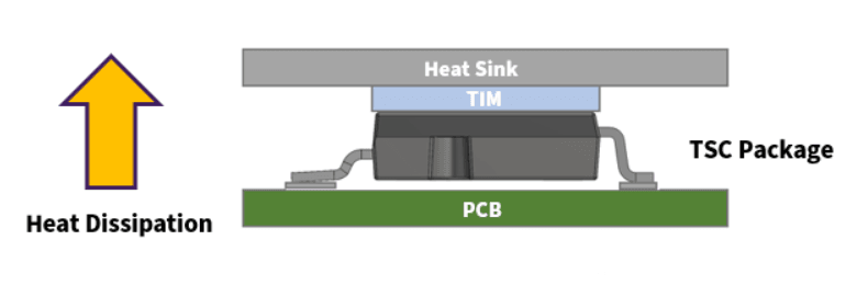
    Most standard surface mount discrete power semiconductors remove heat through the bottom of the device by making direct contact with the power circuit board (PCB), which utilizes a heat sink or cooling plate attached underneath. This method is common across many different power electronics applications, particularly when size and weight requirements do not limit PCB mounting and heat sinks.

    Top side cooled (TSC) devices, on the other hand, dissipate heat through the top side of the package. Inside TSC packages, the die sits upside down in the upper portion of the package to allow heat to flow directly to the top surface. Generally, TSC devices are best suited for high-performance applications such as automotive and e-mobility systems where high-power densities, advanced thermal management solutions, and small footprints are essential. Within these applications, TSC devices help address cooling requirements by enabling maximum power dissipation and optimizing thermal performance.

    TSC designs also allow for dual-side usage of the PCB since the bottom board surface is no longer needed for the heatsink interface. Removing the heatsink from the thermal path not only creates an improved overall system thermal impedance; it also allows for automated assembly, which can increase manufacturing throughput for a more efficient and cost-effective solution.

    Illustration showing how the TSC package can help with heat dissipation

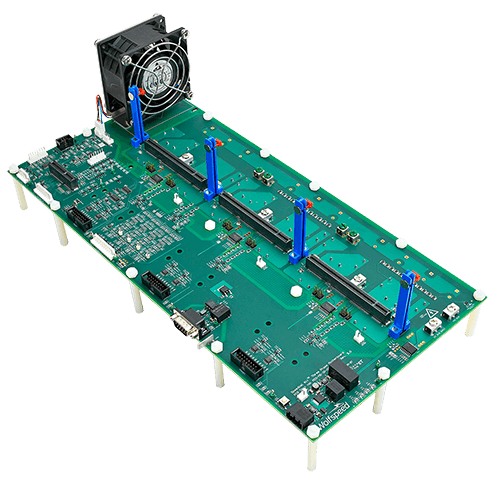
    Evaluating U2 TSC Devices Made Easy with SpeedVal™ Kit

    Wolfspeed’s SpeedVal Kit Modular Evaluation Platform allows engineers to reduce the transition from silicon to silicon carbide (SiC) with a flexible set of building blocks for in-circuit evaluation of system performance at real operating points. The recently released 3-phase motherboard enables high-power testing with static loads as well as a foundation for advanced motor control firmware development.  

    Evaluation boards for a variety of Rdson ratings for Wolfspeed’s TSC MOSFET devices are coming soon.  

    Product photography of a Wolfspeed SpeedVal™ Kit motherboard.
    SpeedVal™ Kit Modular Evaluation Platform​ Three-Phase Motherboard

    Putting U2 TSC Devices to Work: 13 kW Automotive HVAC Motor Drive Reference Design

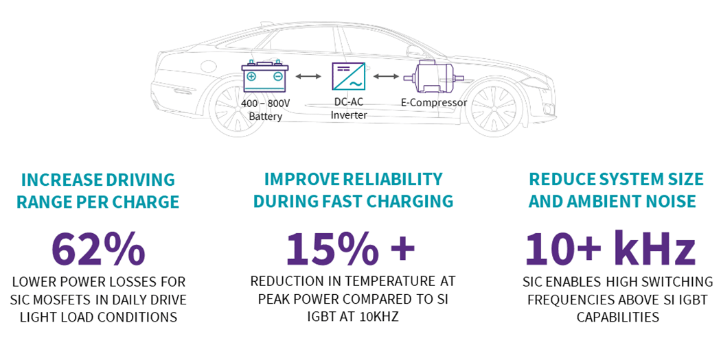
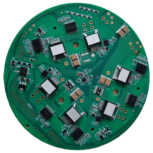
    Wolfspeed’s upcoming 13 kW motor drive reference design, featuring the TSC U2 package, demonstrates the benefits of U2 devices for 10 kW+ EV HVAC systems, which support thermal management of the cabin, battery, and electronics. Optimizing the efficiency and operating temperature range of the HVAC system with the implementation of SiC enables systems designers to bring fast charging to the driver in under 15 minutes, while also extending the driving range per charge for the lifetime of the car. Utilizing Wolfspeed’s new CRD-13DA12N-U2 13 kW HVAC reference design, SiC enables:

    PowerPoint slide showing how the U2 TSC can help increase driving range, improve fast charging, and reduce ambient noise.

    Reference Design Specifications:

    • Input Voltage: 550 – 850 V
    • Max Output Current: 25 A
    • Max Output Power: 13 kW
    • Switching Frequency: 10 – 32 kHz
    • Peak Efficiency: > 98%

    Original – Wolfspeed

    Comments Off on Improve Thermal Management and Conserve Power with Wolfspeed’s New TSC MOSFETs and Schottky Diodes