
-

Toshiba Electronic Devices & Storage Corporation has started mass production of a 3rd generation silicon carbide (SiC) 1200 V and drain current (DC) rating 400 A of SiC MOSFET module “MG400Q2YMS3” for industrial equipment and has expanded its lineup.
The new product MG400Q2YMS3 offers low conduction loss with low drain-source on-voltage (sense) of 0.9 V (typ.). It also offers low switching loss with both turn-on switching loss and turn-off switching loss of 13 mJ (typ.). These help to reduce power loss of equipment and the size of cooling device.
MG400Q2YMS3 has a low stray inductance of 12 nH (typ.) and is capable of high-speed switching. In addition, it suppresses surge voltage in switching operation. Thus, it is available for high frequency isolated DC-DC converter.
Toshiba’s SiC MOSFET module of 2-153A1A package has a lineup of five existing products, MG250YD2YMS3 (2200 V / 250 A), MG400V2YMS3 (1700 V / 400 A), MG250V2YMS3 (1700 V / 250 A), and MG600Q2YMS3 (1200 V / 600 A), including new products. This provides a wider range of product selection.
Toshiba will continue to meet the needs for high efficiency and the downsizing of industrial equipment.
Applications
Industrial equipment
- Auxiliary power supply for railway vehicles
- Renewable energy power generation systems
- Motor control equipment for industrial equipment
- High frequency DC-DC converters, etc.
Features
- Low drain-source on-voltage (sense):
VDS(on)sense=0.9 V (typ.) (ID=400 A, VGS=+20 V, Tch=25 °C) - Low turn-on switching loss:
Eon=13 mJ (typ.) (VDD=600 V, ID=400 A, Tch=150 °C) - Low turn-off switching loss:
Eoff=13 mJ (typ.) (VDD=600 V, ID=400 A, Tch=150 °C) - Low stray inductance:
LsPN=12 nH (typ.)
Original – Toshiba
-

Cambridge GaN Devices (CGD) will take the opportunity afforded by PCIM, Europe’s leading power electronics exhibition and conference (Nuremberg Messe, 11-13th June) to demonstrate how the company’s product portfolio is developing to address higher power applications such as motor drives, inverters and data centres, as well as lower power, ultra-compact smart portable device adapters and chargers.
As well as introducing a new product family, and showing a selection of informative demos on its booth (Hall 7 stand 643), CGD will have a very visible presence around the show with various presentations.
- 15.00, Tuesday 11th June, Hall 9-642: Dr Giorgia Longobardi, CGD’s CEO, will formally launch the company’s latest ICeGaN™ 650V family of GaN ICs, targeting applications in the 1kW to 5kW range.
- 13.30, Tuesday 11th June, Technology Stage (Hall 7 Stand 743): CGD’s CTO, Professor Florin Udrea will take part in a panel discussion hosted by Markt & Technik editor, Engelbert Hopf.
- 14:20, Wednesday 12th June, Technology Stage (Hall 7 booth 743): Professor Udrea will be part of a panel discussion hosted by Bodo’s Power Systems, entitled ‘GaN Wide Bandgap Design, the Future of Power.’
- 14.10, Thursday 13th June, Technology Stage (Hall 7 booth 743): Di Chen, Director of Business Development & Technical Marketing, CGD, and José Quiñones Staff Applications Engineer at Qorvo will share the stage with a joint presentation ‘GaN Power ICs and Power Application Controller Optimize Performance in BLDC and PMSM Motor Drives.’
ANDREA BRICCONI | CHIEF COMMERCIAL OFFICER, CGD
“With its inherent ruggedness and reliability, our ICeGaN™ GaN ICs are perfectly suited to meet the needs of higher power applications such as data centres and inverters. Our presentations and demos and the new devices which we are launching at the show will illustrate our capabilities for these markets.CGD’s Booth (Hall 7 643) will feature reference designs, evaluation boards and demos that support the company’s existing business in chargers and adapters as well as the new higher power applications. New exhibits include:
- Very high power density (30W/in3) 140W reference design produced with the Taiwanese Industrial Technology Research Institute (ITRI) board
- Single leg of a 3-phase automotive inverter demo board, developed in partnership with French public R&I institute, IFP Energies nouvelles
- Two half-bridge evaluation boards with new thermally-enhanced DFN package designs
- A 2.7kW totem-pole power factor correction demo board
- Qorvo motor drive evaluation kit using ICeGaN
- Demo comparing a half-bridge circuit realized using ICeGaN vs discrete e-Mode GaN
ANDREA BRICCONI | CHIEF COMMERCIAL OFFICER, CGD
“The power electronics world has swung irrevocably in favour of GaN. Visit CGD during PCIM to experience the world’s easiest-to-use GaN, so your application can benefit from GaN’s greater efficiency and higher power density now, without any design delays.”Original – Cambridge GaN Devices
-

Ideal Power Inc. announced the successful completion of its qualification of the Company’s second wafer fabrication supplier with high-volume production capability. This facility in Europe adds dual sourcing for wafer fabrication and will support future revenue growth, providing ample capacity to support anticipated customer demand over at least the next two to three years.
“We are delighted to announce this key milestone of qualifying a second high-volume wafer foundry to provide wafer fabrication for our products. This fab successfully completed a multi-wafer full process flow engineering run of double-sided B-TRAN™ wafers. By leveraging our proprietary and proven process flow, this foundry was able to produce functional, bidirectional devices on their initial run without the need for special equipment or capital investment,” said Dan Brdar, President and Chief Executive Officer of Ideal Power.
European wafer fabrication supplier highlights:
- This supplier, along with our previously qualified wafer fabricator in Asia, provides dual sourcing for wafer fabrication in disparate geographies with no exposure to China or Taiwan to mitigate supply chain risk.
- Demonstrated expertise in commercial manufacturing of high power, bipolar devices such as IGBTs. This expertise provides proven process recipes, capability and equipment that can be readily used or adapted for B-TRAN™ double-sided wafer fabrication.
- Qualified manufacturer of semiconductor wafers to multiple Tier 1 automotive suppliers. This will help Ideal Power to attract and engage prospective automotive OEMs and Tier 1 automotive suppliers as customers.
- ISO 9001 and ISO 14001 certified to globally recognized standards for quality and environmental management systems.
Ideal Power’s patented semiconductor power switch, B-TRAN™, can reduce power losses by 50% or more over conventional power switches, depending on the application. B-TRAN™’s higher efficiency results in less heat being generated and therefore significantly lower thermal management requirements, requiring significantly smaller surface area to dissipate heat and giving rise to potentially smaller original equipment manufacturer products.
B-TRAN™ offers the industry’s only symmetric bidirectional operation, reducing the number of components required for an application by 75% compared to a conventional bidirectional switch utilizing IGBTs and diodes. This highly efficient and unique symmetric operation provides a strong competitive advantage in bidirectional applications, which are growing rapidly as transportation electrifies and power generation shifts to renewable energy coupled with energy storage.
Original – Ideal Power
-

ElevATE Semiconductor and GlobalFoundries announced a manufacturing partnership for high-voltage chips produced at GF’s facility in Essex Junction, Vermont. Designed by ElevATE and manufactured at scale by GF on its proven and power-efficient 7HV technology platform, the chips are vital to both commercial semiconductor testing equipment and critical applications for aerospace and defense systems.
The agreement outlines GF’s supply of its 7HV chip technology to ElevATE and the marketplace. Manufactured on 200mm wafers at GF’s Vermont facility, the mature-node chips pair power management and wireless sensing capabilities, delivering the performance, design flexibility and power efficiency required by a range of electronics devices in national security systems. The 7HV platform is optimized for cost and performance, and offers a full suite of features and options with well-characterized design tools, as well as proven manufacturing reliability with robust yields.
To meet the demands of commercial clients and the aerospace and defense industry, ElevATE and GF are collaborating to provide restart support and reestablish the production of 7HV chips. The renewed availability of the 7HV platform will save customers costs, time, and the challenge of redesigning their products using a different chip technology. The new supply will build upon the success of the millions of 7HV chips previously manufactured at GF’s Vermont facility.
“This collaboration marks a significant transformation in ElevATE’s production strategy, transitioning its fabrication processes to GlobalFoundries,” said Anil Kodali, Vice President of Operations and Quality Assurance at ElevATE. “With GF as our manufacturing partner, we can be sure of a robust and reliable source of supply, enabling us to meet the escalating demands of our customers in terms of volume, quality and time-to-market.”
“Our collaboration with ElevATE underscores GF’s commitment to ensuring the U.S. semiconductor and national security ecosystems have a reliable supply of secure, domestically manufactured chips,” said Nicholas Sergeant, vice president and head of the aerospace, defense and critical infrastructure business at GF. “As the leading supplier of essential chips for the U.S. aerospace and defense industry and a longstanding partner to the Department of Defense, GF goes above and beyond to ensure our national security customers have the chips they need, manufactured where they want them, with the right level of security.”
GF’s facility in Essex Junction, Vermont, near Burlington, was among the first major semiconductor manufacturing sites in the United States. Today, around 1,800 GF employees work at the site. Built on GF’s differentiated technologies, these GF-made chips are used in smartphones, automobiles, and communications infrastructure applications around the world. The facility is a DMEA-accredited Trusted Foundry and manufactures secure chips in partnership with the U.S. government.
Original – GlobalFoundries
-
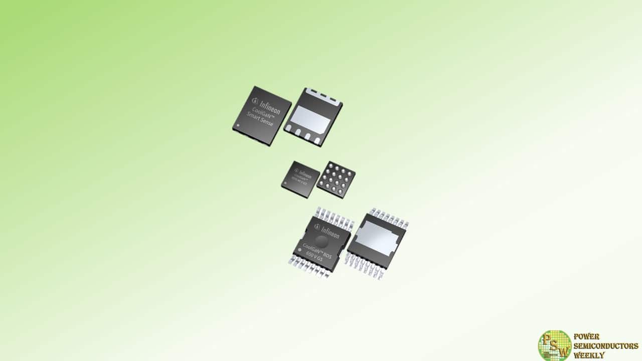
Infineon Technologies AG announced two new CoolGaN™ product technologies, CoolGaN bidirectional switch (BDS) and CoolGaN Smart Sense. CoolGaN BDS provides exceptional soft- and hard-switching behavior, with bidirectional switches available at 40 V, 650 V and 850 V. Target Applications of this family include mobile device USB ports, battery management systems, inverters, and rectifiers.
The CoolGaN Smart Sense products feature lossless current sensing, simplifying design and further reducing power losses, as well as transistor switch functions integrated into one package. They are ideal for usage in consumer USB-C chargers and adapters.
The CoolGaN BDS high voltage will be available at 650 V and 850 V and feature a true normally-off monolithic bi-directional switch with four modes of operation. Based on the gate injection transistor (GIT) technology, the devices have two separate gates with substrate terminal and independent isolated control. They utilize the same drift region to block voltages in both directions with outstanding performance under repetitive short-circuit conditions.
Applications can benefit by using one BDS instead of four conventional transistors, resulting in higher efficiency, density, and reliability. Furthermore, significant cost savings are achieved. The devices optimize performance in the replacement of back-to-back switches in single-phase H4 PFC and HERIC inverters and three-phase Vienna rectifiers. Additional implementations include single-stage AC power conversion in AC/DC or DC/AC topologies.
The CoolGaN BDS 40 V is a normally-off, monolithic bi-directional switch based on Infineon’s in-house Schottky Gate GaN technology. It can block voltages in both directions, and through a single-gate and common-source design, it is optimized to replace back-to-back MOSFETs used as disconnect switches in battery-powered consumer products. The first 40 V CoolGaN BDS product has a 6 mΩ R DS(on), with a range of products to follow. Benefits of using 40 V GaN BDS vs. back-to-back Si FETs include 50 – 75 percent PCB area savings and a reduction of power losses by more than 50 percent, all at a lower cost.
The CoolGaN Smart Sense products feature 2 kV electrostatic discharge withstand and can connect to controller current sense for peak current control and overcurrent protection. The current sense response time is ~200 ns, which is equal or less than common controller blanking time for ultimate compatibility.
Implementing the devices results in increased efficiency and cost savings. At a higher R DSs(on) of e.g. 350 mΩ, the CoolGaN Smart Sense products offer similar efficiency and thermal performance at lower cost compared to traditional 150mΩ GaN transistors. Moreover, the devices are footprint compatible to Infineon’s transistor-only CoolGaN package, eliminating the need for layout rework and PCB respin, and further facilitating design with Infineon’s GaN devices.
Engineering samples of the CoolGaN BDS 40 V are available now for 6 mΩ and will follow in Q3 2024 for 4 mΩ and 9 mΩ. Samples of the CoolGaN BDS 650 V will be available in Q4 2024, and 850 V will follow early 2025. CoolGaN Smart Sense samples will be available in August 2024. Further information is available here: https://www.infineon.com/cms/en/product/promopages/GaN-innovations/
Original – Infineon Technologies
-
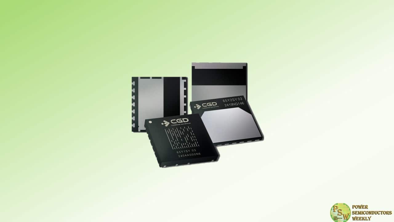
Cambridge GaN Devices (CGD) announced two new packages for the company’s ICeGaN™ family of GaN power ICs that offer enhanced thermal performance and simplify inspection. Variants of the well-proven DFN style, both packages are extremely rugged and reliable.
Developed for CGD, the DHDFN-9-1 (Dual Heat-spreader DFN) is a thin, dual-side cooled package with a small, 10×10 mm footprint and wettable flanks to simplify optical inspection. It offers low thermal resistance (Rth(JC), and can be operated with bottom-side, top-side and dual-side cooling, offering flexibility in design and out-performing the often-used TOLT package in top-side and, especially, dual-side cooled configurations.
The DHDFN-9-1 package has been designed with dual-gate pinout to facilitate optimal PCB layout and simple paralleling, enabling customers to address applications up to 6 kW with ease. The BHDFN-9-1 (Bottom Heat-spreader DFN) is a bottom-side cooled package, also with wettable flanks for easy inspection. Thermal resistance is 0.28 K/W, matching or exceeding other leading devices. Measuring 10×10 mm, the BHDFN is smaller than the commonly-used TOLL package yet shares a similar footprint, hence a common layout with TOLL-packaged GaN power ICs is possible for ease of use and evaluation.
Nare Gabrielyan | Product Marketing Manager, CGD
“These new packages are part of our strategy to enable customers to use our ICeGaN GaN power ICs at higher power levels. Servers, data centres, inverters/motor drives, micro-inverters and other industrial applications are all beginning to enjoy the power density and efficiency benefits that GaN brings, but they are also more demanding. Therefore, it is essential for such applications that devices are also rugged and reliable, and easy to design in. These attributes are inherent in ICeGaN, and are supported and extended by the new packages.”
Improving thermal resistance performance has several benefits. First, more power output is available at the same RDS(on) . Devices also run at cooler temperatures for the same power, so less heatsinking is required, resulting in reduced system costs. Lower operating temperatures also lead to higher reliability and longer lifetimes. Finally, if cost is the constraint for the application, designers can use a lower cost part with a higher RDS(on) and still achieve the required power output.
The new packages will be shown for the first time publicly at the upcoming PCIM exhibition on CGD’s booth # 7 643, Nürnberg Messe, Nuremberg, Germany, 11-13th June 2024.
Original – Cambridge GaN Devices
-
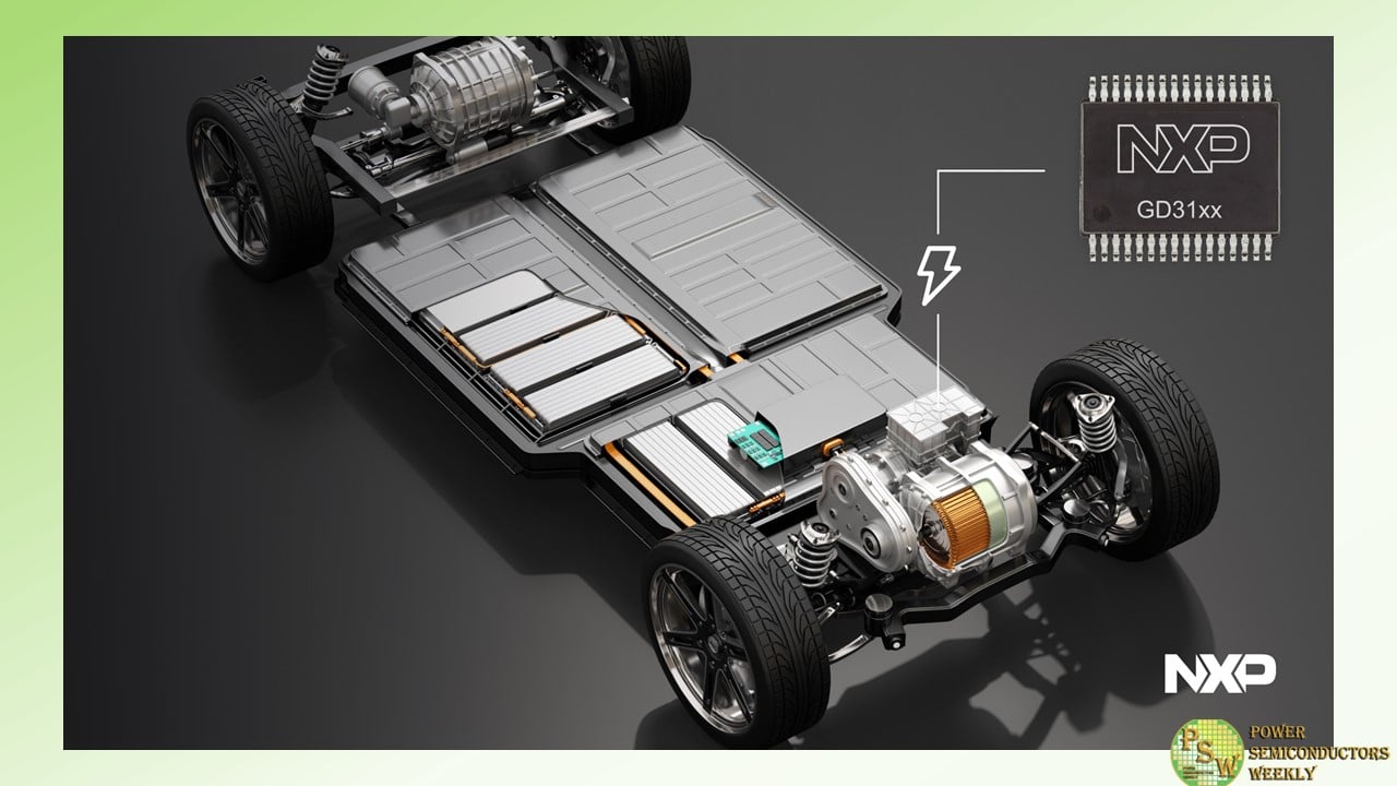
NXP Semiconductors N.V. announced a collaboration with ZF Friedrichshafen AG, a global leader in e-mobility, on next-generation SiC-based traction inverter solutions for electric vehicles (EVs). By leveraging NXP’s advanced GD316x high-voltage (HV) isolated gate drivers, the solutions are designed to accelerate the adoption of 800-V and SiC power devices. Safe, efficient and higher performance traction inverters enabled by the GD316x product family can be designed to extend EV range and reduce the number of charging stops while lowering system level costs for OEMs.
The collaboration between ZF and NXP is a significant step towards accelerating the electrification of the automotive industry, and creating more safe, sustainable, and energy-efficient EVs for the future.
“We look forward to working with NXP to raise the bar for the capabilities and performance of our 800-V traction inverter solutions, which will help us achieve our goals of reducing emissions and promoting sustainability,” said Dr. Carsten Götte, SVP Electrified Powertrain Technology at ZF. “The combination of ZF’s expertise in motor control and power electronics with NXP’s GD316x gate driver family enables us to provide our latest SiC-based traction inverters with higher power and volume density, efficiency and differentiation, and provide our customers with significant safety, efficiency, range and performance improvements.”
Traction inverters are a critical component of an EV’s electric powertrain, converting DC voltage from the battery into a time-varying AC voltage, which drives the vehicle’s motor. As traction inverters now migrate to SiC-based designs, the SiC power devices need to be paired with HV isolated gate drivers to harness the advantages such as higher switching frequency, lower conduction losses, better thermal characteristics and higher robustness at high voltages, compared to previous generation silicon-based IGBT and MOSFET power switches.
The GD316x family of advanced, functionally safe, isolated, high voltage gate drivers incorporates a number of programmable control, diagnostic, monitoring, and protection features, enhanced to drive the latest SiC power modules for automotive traction inverter applications. Its high level of integration allows a smaller footprint and simplifies the system design.
The outstanding capabilities reduce Electromagnetic Compatibility (EMC) noise while also reducing switching energy losses for better efficiency. Fast short-circuit protection times (< 1 µsec) in combination with powerful and programmable gate drive schemes optimize the performance of the traction inverter’s SiC power modules.
“Together with ZF, we are developing next-generation power electronics for future EVs,” said Robert Li, Senior Vice President and General Manager, Electrification at NXP. “Our gate driver family implements a number of outstanding features to both protect and unleash the benefits of high-voltage SiC power switches, making them an ideal choice for ZF’s new SiC-based traction inverter solutions. This collaboration is a testament to our commitment to delivering state-of-the-art solutions that enable OEMs to achieve their EV performance and sustainability goals.”
ZF traction inverters, enabled by NXP’s GD316x product family, are already on the road.
Original – NXP Semiconductors
-

STMicroelectronics and Geely Auto Group have signed a long-term Silicon Carbide (SiC) supply agreement to accelerate their existing cooperation on SiC devices. Under the terms of this multi-year contract, ST will provide multiple Geely Auto brands with SiC power devices for mid-to-high-end battery electric vehicles (BEVs), boosting Geely Auto’s NEV transformation strategy with improved performance, faster charging speeds and extended driving range.
In addition, building on their longstanding cooperation across multiple automotive applications, Geely and ST have established a joint lab to exchange information and explore innovative solutions related to automotive Electronics/Electrical (E/E) architectures (i.e. in-vehicle infotainment, smart cockpit systems), advanced driver assistance (ADAS), and NEVs.
Geely Auto Group has adopted ST’s third generation SiC MOSFET devices in electric traction inverters. The traction inverter is the core of electric powertrains and SiC MOSFETs maximize their efficiency. The combination of advanced inverter design with high-efficiency power semiconductors, like SiC, is the key to superior electric vehicle performance.
“We are very pleased to establish a win-win cooperation with STMicroelectronics, to empower each other and fully utilize our respective advantages and resources.I believe that through the form of innovation joint lab, Geely and ST can deepen our cooperation, achieve mutual benefit, and accelerate the development and implementation of innovative technologies in Geely Auto,” said Li Chuanhai, President of Electronic and Electrical Center of Geely Automotive Central Research Institute.
“We are pleased to have a deep cooperation with global automotive semiconductor leader STMicroelectronics to establish an innovation joint lab. Both sides will deepen long-term cooperation in fields such as smart driving to jointly focus on customer needs, accelerate the implementation of new products and solutions, and shape an efficient cooperation mode. I believe that this cooperation will be beneficial for both parties to conduct more forward-looking technical research based on the development trends of smart, electrified, and connected cars. Geely is delighted to leverage STMicroelectronics’ leading automotive business solutions to be well positioned in product performance, system integration, and overall market competitiveness,” said Fu Zhaohui, Director of the Electronic and Electrical Center of Geely Automotive Central Research Institute.
“Geely Auto, is a shining example of automotive innovation in China, making rapid progress in car electrification and digitalization, while expanding its presence in the global market. This long-term SiC supply agreement and the joint lab establishment mark a significant step forward in our long-established cooperation,” said Henry Cao, Executive Vice President of Sales & Marketing, China Region, STMicroelectronics. “China is the biggest NEV market worldwide and a leading innovator. Our local competence centers and joint labs with our customers across the value chain of automotive allow ST to better support automotive innovation and transformation in China.”
As a leading global automobile manufacturer and China’s top automotive brand, Geely Auto sold a total of 1.68 million vehicles in 2023, with NEV sales reaching 480,000 units, accounting for 28% of the Company’s total sales for the year. This NEV sales volume represents a year-over-year increase of 48%, demonstrating Geely Auto’s successful transition towards NEV and its growing impact in the industry.
With a state-of-the-art SiC manufacturing process and a completely vertically integrated supply-chain, ST provides SiC devices for a wide range of EV applications including traction inverter, OBC (onboard charger), DC-DC converter, EV charging station and e-compressor application, significantly enhancing the performance, efficiency, and range of NEVs. In June 2023, ST and Sanan Optoelectronics, a market leader in compound semiconductors in China, announced the creation of a new 200mm SiC device manufacturing JV in Chongqing, China. This facility will better support the needs of Chinese customers as ST collaborates with more leading Chinese carmakers, industrial customers, and solution providers in SiC, to accelerate the pace of electrification in China.
Original – STMicroelectronics
-

Qorvo® will showcase its latest power management innovations at the upcoming PCIM exhibition and conference from June 11-13 in Nuremberg, Germany. Attendees are invited to visit the Qorvo booth #7-406 to explore the latest advancements in SPICE simulation, silicon carbide (SiC) and motor control technologies.
Qorvo will feature the following at PCIM 2024:
QSPICE™ Simulation Software Showcase
PCIM attendees can experience the next level of simulation with Qorvo’s advanced QSPICE tool during small group Q&A with the tool’s creator, Mike Engelhardt.Training Session Schedule (visit Qorvo booth to confirm training session times)
• Tuesday, June 11, 1:30 p.m.: The QSPICE User Interface
• Wednesday, June 12, 1:30 p.m.: Importing 3rd Party Models
• Thursday, June 13, 10:30 a.m.: Anatomy of a Macro Model Done RightSiC Solutions
Qorvo’s unique cascode JFET configuration delivers industry-leading RDS(on) and best-in-class switching frequency in multi-kilowatt SiC applications across automotive, industrial, renewables and network infrastructure markets. Experts will be on hand to discuss the latest advancements with SiC JFETs, modules and FETs.
Motor Control Solutions
Qorvo’s booth will feature a variety of intelligent motor control solutions that span the input voltage spectrum, including:
• New family of 44V-72V motor controllers with integrated protection features for safety-critical applications like power tools and garden tools
• Robotics demo with partner Tinymvr featuring both Qorvo motor control and battery management solutions
• Wide bandgap showcase with both Qorvo SiC and partner Cambridge GaN Devices (CGD) products paired with high-voltage motor controllersOriginal – Qorvo
-

The electronics industry is witnessing a significant shift towards more compact and powerful systems, driven by technological advancements and a growing focus on decarbonization efforts. With the introduction of the Thin-TOLL 8×8 and TOLT packages, Infineon Technologies AG is actively accelerating and supporting these trends. They enable a maximum utilization of the PCB mainboard and daughter cards, while also taking the system’s thermal requirements and space restrictions into account.
The company is now expanding its portfolio of CoolSiC™ MOSFET discretes 650 V with two new product families housed in the Thin-TOLL 8×8 and TOLT packages. They are based on the CoolSiC Generation 2 (G2) technology, offering significantly improved figures-of-merit, reliability, and ease-of-use. Both product families specifically target high and medium switching-mode power supplies (SMPS), including AI servers, renewable energy, EV chargers, and large home appliances.
The Thin-TOLL package has a form factor of 8×8 mm and offers the best-in-class Thermal Cycling on Board (TCoB) capability on the market. The TOLT package is a top-side cooled (TSC) enclosure with a similar form factor to TOLL. Both package types offer developers several benefits: Using them in AI and server power supply units (PSU), for example, reduces the thickness and length of the daughter cards and allows for a flat heat sink.
When used in microinverters, 5G PSU, TV PSU and SMPS, the Thin-TOLL 8×8 package allows for a minimization of the PCB area occupied by the power supply devices on the mainboard, while TOLT keeps the junction temperature of the devices under control, given that these applications typically use convection cooling. In addition, TOLT devices complete Infineon’s top-side cooled CoolSiC industrial portfolio, namely CoolSiC 750 V in Q-DPAK. They enable developers to reduce the PCB footprint occupied by SiC MOSFETs when the power to be delivered to the devices does not require a Q-DPAK package.
The CoolSiC MOSFETs 650 V G2 in ThinTOLL 8×8 and TOLT are now available in R DS(on) from 20, 40, 50 and 60 mΩ. Additionally, the TOLT variant is also available with an R DS(on) of 15 mΩ. The product family will be expanded by a more granular portfolio by the end of 2024. More information is available at www.infineon.com/coolsic-gen2. Infineon will showcase the CoolSiC MOSFET 650 V Generation 2 at the PCIM in Nuremberg.
Original – Infineon Technologies