-

Toshiba Electronic Devices & Storage Corporation and Toshiba Corporation (Toshiba Group) have developed technology that mitigates the parasitic oscillation that occurs during switching operations by power modules with silicon carbide (SiC) MOSFETs connected in parallel, even with a 60% smaller gate resistance than is typical. The technology reduces power loss in power modules, mitigates oscillation, and realizes highly reliable switching operations.
The drive for carbon neutrality is stimulating demand for technologies that improve energy efficiency in many areas, including renewables, railways, and industrial equipment. In these sectors, the application of power modules built around SiC MOSFETs is seen as a solution that supports high-speed switching at high voltages and large currents—which is particularly important for the miniaturization of power converters, where higher switching frequencies result in higher rates of switching losses against power consumption.
Connecting multiple chips in parallel in power modules can form oscillation circuits, the result of wiring inductance between the chips and their parasitic capacitance. It can reduce module reliability if not countered, which is usually done by increasing gate resistance. However, this approach slows switching speed, resulting in a trade-off with switching losses. For power modules with SiC MOSFETs to perform high-speed switching, another approach is needed.
Toshiba Group used an equivalent circuit model of the power module (Figure 1) to determine the theoretical condition that triggers parasitic oscillation, and developed a wiring layout less likely to cause it. This was done by analyzing simulations of parasitic oscillation occurs when Lg/Ls, the ratio of gate-to-gate inductance Lg and source-to-source inductance Ls of parallel chips, is below a certain value (Figure 2). As increasing Lg/Ls is an effective means of mitigating parasitic oscillation, Toshiba Group fabricated prototype modules with different Lg/Ls and measured switching. This confirmed that increasing Lg/Ls mitigated oscillation, even with a 60% smaller gate resistance than that required by the alternative approach of increasing gate resistance (Figure 3).
Applying this approach to oscillation mitigation in power modules now under development has realized a power module less likely to cause parasitic oscillation, even with minimal gate resistance, that achieves low power loss with mitigated oscillation, and delivers highly reliable switching operation. Toshiba Group will continue to make refine the modules toward an early product launch.
Toshiba Group presented the details of this technology on June 6 at the 36th International Symposium on Power Semiconductor Devices and ICs (ISPSD) 2024, an international power semiconductor conference held in Bremen, Germany from June 2 to 6.
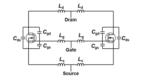
Figure 1. Model equivalent circuit of two MOSFETs connected in parallel 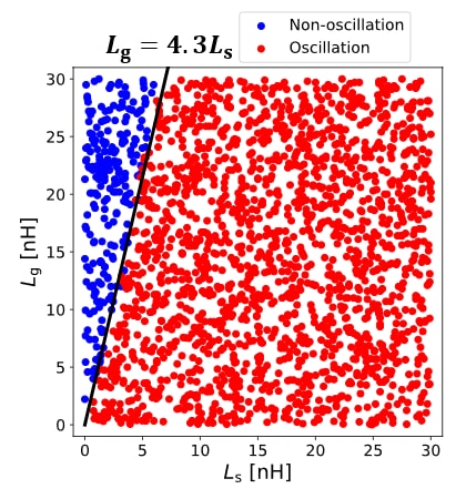
Figure 2. Simulation of oscillation in two MOSFETs with zero gate resistance connected in parallel 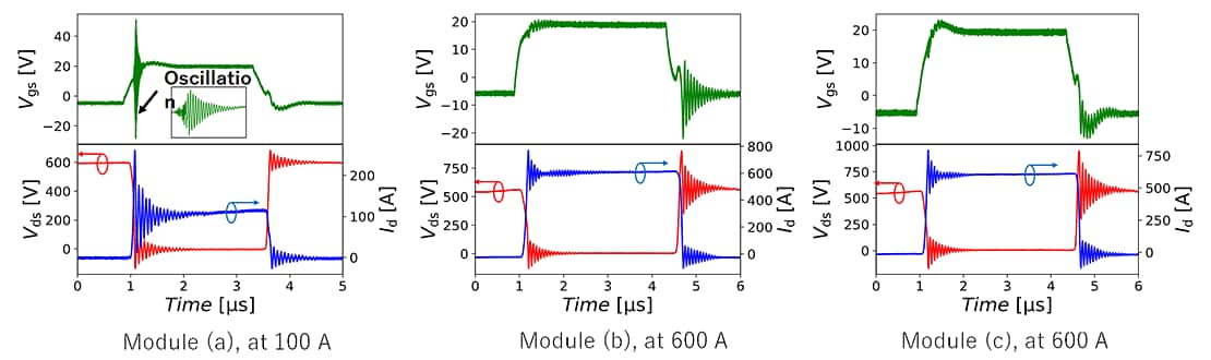
Vgs: Gate-Source voltage, Vds: Drain-Source voltage, Id: Drain current
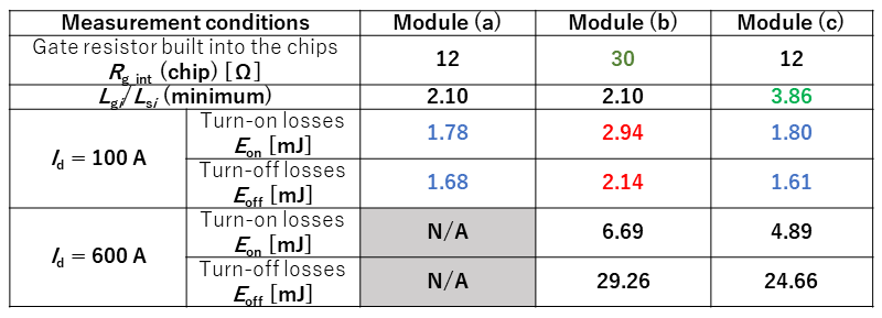
Figure 3. Switching waveforms and switching losses of the prototype modules (Source: Toshiba Group tests) Original – Toshiba
-

Infineon Technologies AG expanded the lawsuit pending before the District Court for the Northern District of California on 23 July 2024, adding claims against Innoscience (Zhuhai) Technology Company, Ltd., and Innoscience America, Inc. and affiliates based on the infringement of three additional patents referring to gallium nitride (GaN) technology owned by Infineon. In addition, Infineon today filed a complaint with the U.S. International Trade Commission (USITC) containing legal claims referring to the same four patents covered by the lawsuit.
Infineon seeks a permanent injunction for the infringement of United States patents referring to gallium nitride (GaN) technology owned by Infineon. The patent claims cover core aspects of GaN power semiconductors encompassing innovations that enable performance and reliability of Infineon’s proprietary GaN power transistors.
Already, on 14 March 2024, Infineon filed a patent infringement suit against Innoscience in the United States with the District Court for the Northern District of California. On 4 June 2024, Infineon filed a corresponding lawsuit with the District Court Munich, Germany. Additional lawsuits were filed against distributors of Innoscience in Germany.
Furthermore, Infineon successfully filed for a preliminary injunction (court order), which the District Court Munich issued on 12 June 2024. According to this court order Innoscience was obligated to remove all infringing product from their booth at the international power electronics trade show PCIM Europe.
Infineon leads the industry with its GaN patent portfolio, comprising approximately 350 patent families. Infineon’s portfolio of silicon, silicon carbide, gallium nitride power transistors and complementary drivers and controllers was enhanced with the October 2023 acquisition of GaN Systems Inc. The acquisition boosted Infineon’s GaN offering and further expanded its leading position in power semiconductors.
Original – Infineon Technologies
-

MCC introduced the latest additions to its robust portfolio: 10 1200V SiC N-channel MOSFETs in versatile TO-247-4, TO-247-4L, and TO-247AB packages. These new MOSFETs are available in 3-pin and 4-in (Kelvin source) configurations and meet the rising demand for high-power, high-voltage applications.
Boasting exceptional on-resistance values from 21mΩ to 120mΩ (typ.) and fast switching speeds, these components are the ones you can count on for reliable performance. Their excellent thermal properties and fast intrinsic body diode ensure smooth, efficient operation in the most challenging conditions, making them a must-have for critical power systems.
Features & Benefits:
- High-power capability: 1200V MOSFET with SiC technology
- Fast, reliable switching: Intrinsic body diode improves efficiency & ruggedness Enhanced performance: High switching speed with low gate charge
- Wide on-resistance selection: ranging from 21mΩ to 120mΩ (typ.)
- Efficiency: Superior thermal properties and low switching losses
- Durability: Avalanche ruggedness
- Versatility: TO247 3-pin and 4-pin package options
Original – Micro Commercial Components
-

Power Master Semiconductor (PMS) announced the release of its new AEC-Q101 qualified 1200V eSiC MOSFET in a D2PAK-7L package, designed to revolutionize power electronics in electric vehicles (EVs). PMS’s automotive-grade 1200V eSiC MOSFET offers superior efficiency, high power density, high reliability, and enables bi-directional operation, making it an ideal choice for a wide range of automotive applications, including on-board chargers (OBCs), DC-DC converters, and e-compressors.
The automotive industry is rapidly transitioning towards electrification, driven by the growing demand for sustainable and environmentally friendly transportation solutions. This shift has created a surge in demand for high-performance power electronics that can meet the stringent requirements of EV applications. Bi-directional operation is the key trend for the on-board chargers (OBCs) applications to meet V2L (Vehicle to Load), V2G (Vehicle to Grid), V2V (Vehicle to Vehicle), and V2H (Vehicle to Home appliance).
Therefore, the topology of OBCs is moving to Totem-pole PFC + CLLC or DAP resonant converter from Interleaved CCM PFC or Dual boost bridgeless PFC + LLC resonant converters. Larger battery capacity and faster charging demands are driving 800V battery systems for BEV application.
The automotive grade 1200V eSiC MOSFET is an optimized solution for the e-compressor, an indispensable power conversion system for efficient thermal management that increases battery life, charging efficiency, and driving range, and maintains a comfortable environment. It is also optimized for Totem-Pole PFC and CLLC/DAB (Dual Active Bridge) topologies, which are essential for bidirectional power conversion, a key trend in onboard chargers (OBC) for 800V battery system in electric vehicles.
Key Features of automotive grade 1200V e SiC MOSFET
- AEC-Q101 qualified for automotive applications
- Robust Avalanche Capability
- 100% Avalanche Tested
- Operating temperature range : -55°C to +175°C
- Low switching losses
- D2PAK-7L kelvin source package for ease of design and integration
“Driven by our unwavering commitment to innovation and sustainability, Power Master Semiconductor continuously develops power device solutions that achieve breakthrough efficiency and performance”, said Namjin Kim, Senior Director of Sales & Marketing.” The introduction of our new automotive-grade 1200V eSiC MOSFET represents a major leap forward in empowering the automotive industry’s shift towards cleaner, more energy-efficient power electronics. We are confident that this innovative solution will be the optimal choice for high-performance automotive applications.”
Original – Power Master Semiconductor
