-
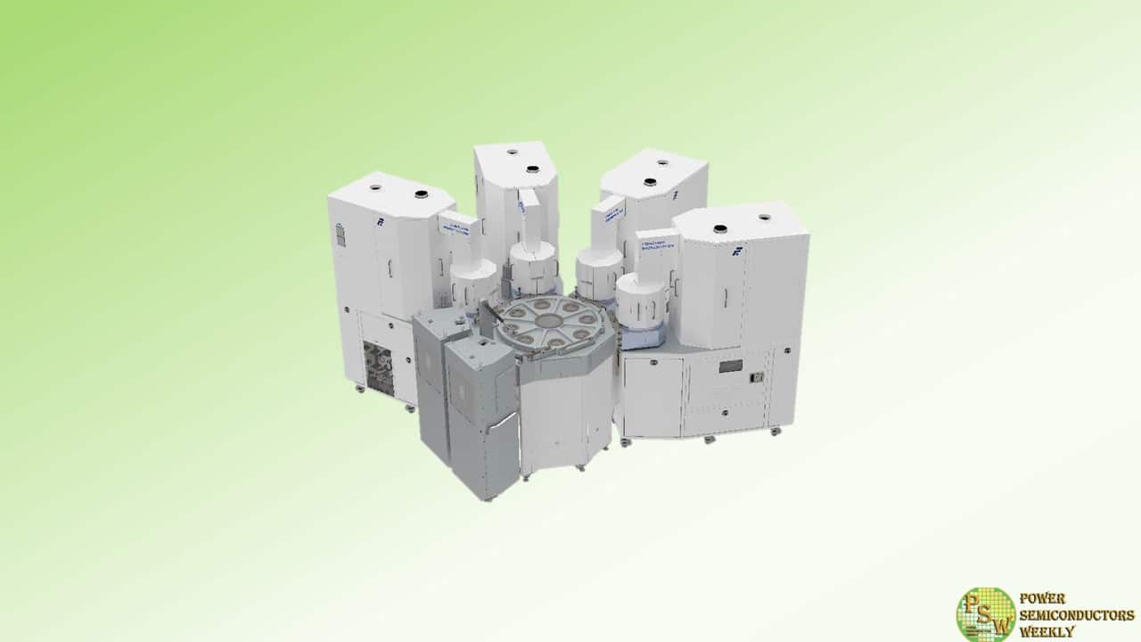
Forge Nano, Inc., a leading ALD equipment provider and materials science company, further expanded into the semiconductor market with the unveiling of its new Atomic Layer Deposition (ALD) product offering – TEPHRA™ – Forge Nano’s new single-wafer, ALD cluster platform. By offering single-wafer ALD coating quality at throughputs similar to the speed of batch systems, Forge Nano’s TEPHRA ™ will allow customers to produce best-in-class coatings at commercial scale with unrivaled precursor efficiency and speed.
Powered by Forge Nano’s ALDx technology, which offers ultrathin, uniform, pinhole-free films with an unprecedented 10x throughput for single-wafer processing, TEPHRA is dedicated to the manufacturing of specialty semiconductor applications on 200mm wafers and below. With 100x efficient chemical use, rapid cycle times, increased yield, and low-risk manufacturing, TEPHRA is the only single-wafer cluster tool with commercial throughput speeds serving applications in advanced packaging, power semiconductor, radio frequency devices (RFD), microLEDs, microelectromechanical systems (MEMS), and more.
“TEPHRA is designed to unlock new capabilities to meet the growing demand of novel More-than-Moore market device applications that seek high-throughput ALD capabilities without sacrificing film qualities. Forge Nano will enable advanced device architectures with groundbreaking efficiency in the semiconductor space with our innovative ALD wafer tools that prioritize cost, performance and efficiency,” said Paul Lichty, CEO of Forge Nano. “With TEPHRA, Forge Nano is opening new coating solutions and opportunities for our proprietary coating techniques that address high aspect ratio structures, which have previously been underserved in the semiconductor industry.”
Forge Nano’s ALDx technology enables conformal coatings to scale to aspect ratios greater than 10:1. With a flagship all-ALD Metal Barrier Seed film application, TEPHRA offers nitride and metal depositions in high aspect ratio structures for advanced 3D integration applications, including through silicon and through glass vias. By moving beyond 10:1 aspect ratios, manufacturers can scale their packaging processes and reduce power consumption by overcoming common pitfalls of directional deposition technologies, including PEALD, which struggle with conformality and void formation.
TEPHRA is available in a range of configurations with the option for four-sided, six-sided and eight-sided cluster platforms. TEPHRA can process wafers up to 200 mm between 80 and 300°C with six process precursor channels and dedicated chambers for oxide, nitride and metal depositions. TEPHRA ™ also features Forge Nano’s patented CRISP technology, a suite of catalyzed thermal ALD processes that enable low temperature and hard-to-deposit materials without the need for plasma.
For more information on Forge Nano’s TEPHRA ™ product, visit the TEPHRA product page at: https://www.forgenano.com/products/tephra. SEMICON West 2024 attendees can stop by the Forge Nano booth (#133), located in the south exhibition hall, for additional product information and to discuss capabilities with our product specialists.
Original – Forge Nano
-

GlobalFoundries announced that it has acquired Tagore Technology’s proprietary and production proven Power Gallium Nitride (GaN) IP portfolio, a high-power density solution designed to push the boundaries of efficiency and performance in a wide range of power applications in automotive, internet of things (IoT) and artificial intelligence (AI) datacenter. As the digital world continues to evolve with technologies like Generative AI, GaN stands out as a pivotal solution for sustainable and efficient power management particularly in datacenters.
Today’s announcement reinforces GF’s commitment to large-scale manufacturing of GaN technology that offers a suite of benefits to help datacenters meet the increasing power demands while maintaining or improving power efficiency, reducing costs and managing heat generation. The acquisition expands GF’s power IP portfolio and broadens access to market leading GaN IP that will enable GF customers to quickly bring differentiated products to market. As a part of the acquisition, a team of experienced engineers from Tagore, dedicated to the development of GaN technology, will be joining GF.
“We are committed to being the foundation of our customers’ power applications today and for decades to come,” said Niels Anderskouv, chief business officer at GF. “With this acquisition, GF takes another step toward accelerating the availability of GaN and empowering our customers to build the next generation of power management solutions that will reshape the future of mobility, connectivity and intelligence.”
“The accelerating demand for more power efficient semiconductors is dramatically increasing, and Tagore has been at the forefront of developing disruptive solutions using GaN technology for a wide range of power devices,” said Amitava Das, co-founder and chief operating officer of Tagore Technology. “The team and I are excited to join GlobalFoundries to increase our focus on market-leading IP that will help address power design challenges and support the continued evolution of automotive, industrial and AI datacenter power delivery systems.”
In February 2024, GF was awarded $1.5 billion in direct funding under the U.S. CHIPS and Science Act, part of that investment is targeted towards enabling the high-volume manufacturing of critical technologies including GaN to securely produce more essential chips.
Combining this manufacturing capacity with the technical know-how of the Tagore team, GF is set to transform AI system efficiency, especially in edge or IoT devices, where reduced power consumption is critical.
“GlobalFoundries is at the forefront of technological advancements. With Tagore Technology joining the GF India team, we will further enhance our tech capabilities, particularly in emerging areas like GaN,” said Jitendra Chaddah, vice president and India country head at GF. “I welcome the Tagore team to GF, and I am excited about the work we will do as we continue to grow and strengthen our engineering capabilities together.”
Original – GlobalFoundries
