-

ROHM announced the adoption of power modules equipped with 4th generation SiC MOSFET bare chips for the traction inverters in three models of ZEEKR EV brand from Zhejiang Geely Holding Group (Geely), a top 10 global automaker. Since 2023, these power modules have been mass produced and shipped from HAIMOSIC (SHANGHAI) Co., Ltd. – a joint venture between ROHM and Zhenghai Group Co., Ltd. to Viridi E-Mobility Technology (Ningbo) Co., Ltd, a Tier 1 manufacturer under Geely.
Geely and ROHM have been collaborating since 2018, beginning with technical exchanges, then later forming a strategic partnership focused on SiC power devices in 2021. This led to the integration of ROHM’s SiC MOSFETs into the traction inverters of three models: the ZEEKR X, 009, and 001. In each of these EVs, ROHM’s power solutions centered on SiC MOSFETs play a key role in extending the cruising range and enhancing overall performance.
ROHM is committed to advancing SiC technology, with plans to launch 5th generation SiC MOSFETs in 2025 while accelerating market introduction of 6th and 7th generation devices. What’s more, by offering SiC in various forms, including bare chips, discrete components, and modules, ROHM is able to promote the widespread adoption of SiC technology, contributing to the creation of a sustainable society.
Original – ROHM
-

STMicroelectronics has joined Quintauris GmbH as its sixth shareholder. ST joins other Quintauris shareholders, Robert Bosch GmbH, Infineon Technologies AG, Nordic Semiconductor ASA, NXP® Semiconductors, and Qualcomm Technologies, Inc.
Quintauris was founded in December 2023 to advance the adoption of products based on RISC-V principles. This will include access to reference architectures, and assistance in the creation of versatile, cross-industry solutions. The initial core industry applications will be for the automotive sector, with a planned expansion to mobile and IoT.
RISC-V is an open-standard Instruction Set Architecture (ISA), originally developed by researchers at the University of California, Berkeley, in 2010.
“ST is a welcome addition to our list of shareholders,” said Alexander Kocher, CEO, Quintauris.“By fostering collaboration between the world’s largest semiconductor companies, we aim to explore and unlock the potential of RISC-V for all the industries we will serve.”
Original – STMicroelectronics
-
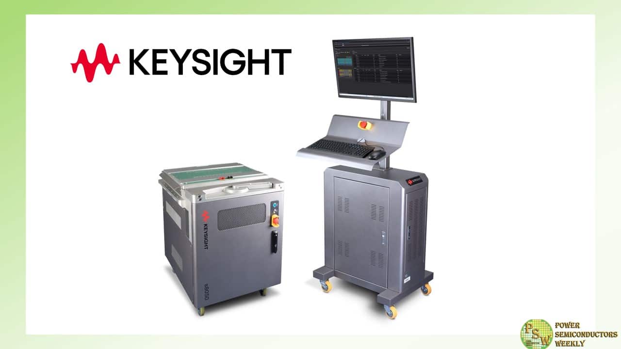
Keysight Technologies, Inc. introduces the Electrical Structural Tester (EST), a wire bond inspection solution for semiconductor manufacturing that ensures the integrity and reliability of electronic components.
The semiconductor industry is faced with testing challenges due to the increasing density of chips in mission-critical applications such as medical devices and automotive systems. Current testing methodologies often fall short in detecting wire bond structural defects, which lead to costly latent failures. In addition, traditional testing approaches frequently rely on sampling techniques that do not adequately identify wire bond structural defects.
The EST addresses these testing challenges by using cutting-edge nano Vectorless Test Enhanced Performance (nVTEP) technology to create a capacitive structure between the wire bond and a sensor plate. Using this method the EST can identify subtle defects such as wire sag, near shorts, and stray wires to enable a comprehensive assessment of wire bond integrity.
Key benefits of the EST include:
- Advanced defect detection – Identifies a wide range of wire bond defects, both electrical and non-electrical, by analyzing changes in capacitive coupling patterns to ensure the functionality and reliability of electronic components.
- High-volume manufacturing ready – Enables throughput of up to 72,000 units per hour through the ability to test up to 20 integrated circuits simultaneously, which boosts productivity and efficiency in high-volume production environments.
- Big data analytics integration: Captures defects and enhances yield through advanced methods like marginal retry test (MaRT), dynamic part averaging test (DPAT), and real-time part averaging test (RPAT).
Carol Leh, Vice President, Electronic Industrial Solutions Group Center of Excellence, Keysight, said: “Keysight is dedicated to pioneering innovative solutions that address the most pressing challenges in the wire bonding process. The Electrical Structural Tester empowers chip manufacturers to enhance production efficiency by rapidly identifying wire bond defects, ensuring superior quality and reliability in high-volume manufacturing.”
The Electrical Structural Tester will be showcased at the Keysight booth (K3283) at SEMICON Taiwan 2024, Taipei Nangang Exhibition Center Hall 1, September 4-6, 2024.
Original – Keysight Technologies
-
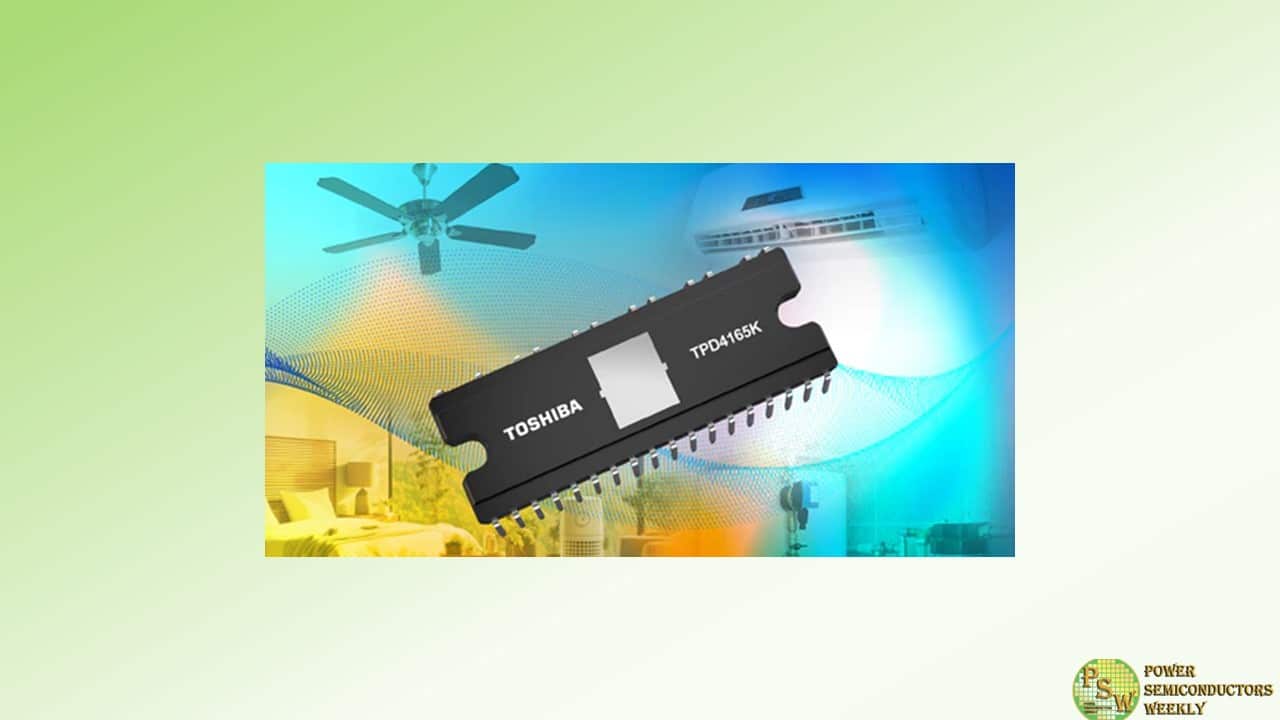
Toshiba Electronics Europe GmbH has launched a small new intelligent power device (IPD) for space-constrained brushless DC (BLDC) motor drive applications such as air conditioners, air purifiers, and pumps.
The new IPD (TPD4165K) has an increased maximum output current of 3A, compared to the 2A rating of Toshiba’s existing products like TPD4163K, or TPD4164K. This extends the range of supported equipment and allows use in higher power applications. The device is suitable for sine-wave drive.
As power supply voltage may fluctuate significantly in some regions where the IP could be used, the absolute maximum voltage rating (VBB) has been increased to 600V to enhance long-term reliability. This represents a 20% increase over Toshiba’s previous products (TPD4123K, TPD4123AK, TPD4144K, TPD4144AK, TPD4135K, TPD4135AK).
The new TPD4165K is housed in a through-hole HDIP30 package. This has a 21% smaller footprint than the DIP26 package used for many of Toshiba’s previous products, simplifying the design process for challenging space-constrained applications. The new device measures just 32.8mm x 13.5mm x 3.525mm. It supports either three-shunt or single-shunt resistor circuit for current sensing.
Built into the new IPD is a range of safety features including over-current, under-voltage and thermal shutdown. Additionally, an external signal can be applied to the SD pin to control the behaviour of the output stage. The DIAG output pin provides the status of the safety conditions.
Designers can freely access a reference design for a sensorless BLDC motor drive circuit based upon the new TPD4165K and Toshiba’s TMPM374FWUG microcontroller with vector control engine capability. The reference design data can be downloaded from Toshiba’s website.
Toshiba will continue to expand its product range by adding devices with improved characteristics. This will assist designers by improving design flexibility as well as contributing to carbon neutrality through energy-saving motor control.
Original – Toshiba
-

onsemi released the newest generation silicon and silicon carbide hybrid Power Integrated Modules (PIMs) in an F5BP package, ideally suited to boost the power output of utility-scale solar string inverters or energy storage system (ESS) applications. Compared to previous generations, the modules offer increased power density and higher efficiencies within the same footprint to increase the total system power of a solar inverter from 300kW up to 350kW.
This means a one-gigawatt (GW) capacity utility-scale solar farm using the latest generation modules can achieve an energy savings of nearly two megawatts (MW) per hour or the equivalent of powering more than 700 homes per year. Additionally, fewer modules are required to achieve the same power threshold as the previous generation, which can reduce power device component costs by more than 25%.
With solar power having achieved the lowest levelized cost of energy (LCOE), it is increasingly becoming the go-to source for renewable power generation around the world. To compensate for solar power’s variability, utility operators are also adding large-scale battery energy storage systems (BESS) to ensure a stable energy flow to the grid. To support this combination of systems, manufacturers and utilities require solutions that offer maximum efficiency and reliable power conversion. Every 0.1% of efficiency improvement can equate to a quarter of a million dollars in annual operational savings for every one gigawatt of installed capacity.
“As a variable energy source dependent on sunlight, continual advances in increasing system efficiencies, reliability and advanced storage solutions are needed to be able to maintain the stability and reliability of global grids during peak and off-peak power demand,” said Sravan Vanaparthy, vice president, Industrial Power Division, Power Solutions Group, onsemi. “A more efficient infrastructure increases adoption and assures us that, as more solar power generation is built out, less energy is wasted and pushes us forward on a path away from fossil fuels.”
The F5BP-PIMs are integrated with 1050V FS7 IGBT and the 1200V D3 EliteSiC diode to form a foundation that facilitates high voltage and high current power conversion while reducing power dissipation and increasing reliability. The FS7 IGBTs offer low turn-off losses and reduce switching losses by up to 8%, while the EliteSiC diodes provide superior switching performance and lower voltage flicker by 15% compared to previous generations.
These PIMs employ an innovative I-type Neutral Point Clamp (INPC) for the inverter module and a flying capacitor topology for the boost module. The modules also use an optimized electrical layout and advanced Direct Bonded Copper (DBC) substrates to reduce stray inductance and thermal resistance. In addition, a copper baseplate further decreases thermal resistance to the heat sink by 9.3%, ensuring the module remains cool under high operational loads. This thermal management is crucial in maintaining the efficiency and longevity of the modules, making them highly effective for demanding applications that require reliable and sustained power delivery.
Original – onsemi
-

PANJIT announced a strategic partnership with National Kaohsiung University of Science and Technology (NKUST). This collaboration bridges the gap between academia and industry, marking a significant step in semiconductor talent development.
Through this partnership, PANJIT and NKUST will establish a comprehensive platform that connects the educational and industrial spheres. PANJIT will offer NKUST students extensive industry insights and internship opportunities, allowing them to apply their theoretical knowledge in real-world settings.
Champion Microelectronic Corp., a member of the PANJIT Group, will collaborate with Professors Jenn-Yu Lin and Cheng-Liang Huang of NKUST’s Department of Microelectronics Engineering and their students on a high-end IC product development project targeting the automotive, industrial control, and automated factory sectors. This initiative aims to meet the growing demand for high-end semiconductors in the global green energy market.
Jason Fang, President of PANJIT Group, stated, “PANJIT is dedicated to building a tier 1 international corporation that our employees are proud of while fostering social engagement. Cultivating talent is a key part of this vision and essential for sustainable industrial development. We believe that a close partnership with academia can drive innovation and accelerate industry progress. In terms of our ESG development strategy, we strive to balance environmental protection, social responsibility, and corporate governance. We are actively engaged in green initiatives, including renewable energy projects, afforestation, forest ecosystem conservation, connecting with local culture and nurturing talent, creating a pleasant work environment for employees, and upholding core values of integrity. More importantly, we aim to pass on PANJIT’s values and technologies to future generations, working together toward a more sustainable future.”
President Ching-Yu Yang of National Kaohsiung University of Science and Technology (NKUST) pointed out that “the establishment of world-class companies in Kaohsiung and the active moves by top universities in the north to enter Kaohsiung are positive signals for the development prospects of the Southern Semiconductor S Corridor. NKUST has long been deeply rooted in southern Taiwan, establishing close cooperative relationships with various industries.
In the trend of rapid industrial transformation towards intelligence and automation, the direction of technological application and talent cultivation must closely align with industrial development trends to strengthen long-term industrial competitiveness. The two key factors in strengthening Taiwan’s industrial competitiveness are technology and talent. Recently, NKUST received a grant of more than NT$100 million from the Ministry of Education to build a “Semiconductor Process Equipment Technology Talent Training Base” in the Department of Microelectronics Engineering of College of Electrical Engineering and Computer Science to strengthen the cultivation of semiconductor technology talents.
Now, the cooperation between NKUST and the PANJIT Group can create mutual benefits in the two critical areas of research/development applications and talent cultivation. ”President Ching-Yu Yang is very much looking forward to deepening the cooperation between the two parties in the future. He stated, “Playing the role of a strong supporter in national industrial research & development and talent cultivation is an unshakable mission for NKUST.”
This collaboration extends beyond talent development to include technology exchange, setting a precedent for future industry-academia partnerships and encouraging more enterprises and institutions to contribute to nurturing the next generation of talent.
Original – PANJIT International
-

MCC Semi unveiled a new 950V MOSFET – MCU1K4N95SH. While traditional MOSFETs often include energy losses and slower switching, this new superjunction (SJ) MOSFET features a low gate-to-drain charge, significantly reducing conduction losses and amplifying overall efficiency.
Its superjunction MOSFET technology and on-resistance of only 1.49Ω empower engineers to design for higher voltage ratings without compromising performance. A DPAK (TO-252) package only adds to this MOSFET’s versatility, making it ideal for AC-DC power supplies, LED lighting, charging adapters, solar and energy devices, and other high-voltage applications across multiple industries.
Features & Benefits:
- Superjunction (SJ) MOSFET technology enhances efficiency
- High-voltage rating of 950V is well-suited for demanding applications
- Low gate charge enables faster switching speeds
- High-speed switching capabilities improve overall performance
Original – Micro Commercial Components
-

Wolfspeed, Inc. announced its results for the fourth quarter of fiscal 2024 and the full 2024 fiscal year.
Quarterly Financial Highlights (Continuing operations only. All comparisons are to the fourth quarter of fiscal 2023.)
- Consolidated revenue of approximately $201 million, as compared to approximately $203 million
- Mohawk Valley Fab contributed approximately $41 million in revenue
- Power device design-ins of $2.0 billion
- Quarterly design-wins of $0.5 billion
- GAAP gross margin of 1%, compared to 29%
- Non-GAAP gross margin of 5%, compared to 31%
- GAAP and non-GAAP gross margins for the fourth quarter of fiscal 2024 include the impact of $24 million of underutilization costs. See “Start-up and Underutilization Costs” below for additional information.
Full Fiscal Year Financial Highlights (all comparisons are to fiscal 2023)
- Consolidated revenue of approximately $807 million, as compared to approximately $759 million
- GAAP gross margin of 10% as compared to 32%
- Non-GAAP gross margin of 13% as compared to 35%
- GAAP and non-GAAP gross margins for fiscal 2024 include the impact of approximately $124 million of underutilization costs. See “Start-up and Underutilization Costs” below for additional information.
“We have two priorities we are focused on: optimizing our capital structure for both the near term and long term and driving performance in our state-of-the-art, 200-millimeter fab, and this quarter was a step forward on both of these priorities,” said Wolfspeed CEO, Gregg Lowe.
“We achieved 20% utilization at Mohawk Valley in June and continued to see strong revenue growth from that fab. Our 200mm device fab is currently producing solid results, which are at significantly lower costs than our Durham 150mm fab. This improved profitability gives us the confidence to accelerate the shift of our device fabrication to Mohawk Valley, while we assess the timing of the closure of our 150mm device fab in Durham. At the JP, we have also made great progress, installing and activating initial furnaces in the fourth quarter. We have already processed the first silicon carbide boules from the JP and the quality is in line with the high-quality materials coming out of Building 10.
“At the same time, we are taking proactive steps to slow down the pace of our CapEx by approximately $200 million in fiscal 2025 and identify areas across our entire footprint to reduce operating costs. We also remain in constructive talks with the CHIPS office on a Preliminary Memorandum of Terms for capital grants under the CHIPS Act. In addition to any potential capital grants from the CHIPS program, our long-term CapEx plan is expected to generate more than $1 billion in cash refunds from Section 48D tax credits from the IRS, of which we’ve already accrued approximately $640 million on our balance sheet,” continued Lowe.
Business Outlook:
For its first quarter of fiscal 2025, Wolfspeed targets revenue from continuing operations in a range of $185 million to $215 million. GAAP net loss is targeted at $226 million to $194 million, or $1.79 to $1.54 per diluted share. Non-GAAP net loss from continuing operations is targeted to be in a range of $138 million to $114 million, or $1.09 to $0.90 per diluted share.
Targeted non-GAAP net loss excludes $88 million to $80 million of estimated expenses, net of tax, primarily related to stockbased compensation expense, amortization of discount and debt issuance costs, net of capitalized interest, project, transformation and transaction costs and loss on Wafer Supply Agreement.
The GAAP and non-GAAP targets from continuing operations do not include any estimated change in the fair value of the shares of common stock of MACOM Technology Solutions Holdings, Inc. (MACOM) that we acquired in connection with the sale to MACOM of our RF product line (RF Business Divestiture).
Start-up and Underutilization Costs:
As part of expanding its production footprint to support expected growth, Wolfspeed is incurring significant factory start-up costs relating to facilities the Company is constructing or expanding that have not yet started revenue generating production. These factory start-up costs have been and will be expensed as operating expenses in the statement of operations.
When a new facility begins revenue generating production, the operating costs of that facility that were previously expensed as start-up costs are instead primarily reflected as part of the cost of production within the cost of revenue, net line item in our statement of operations. For example, the Mohawk Valley Fab began revenue generating production at the end of fiscal 2023 and the costs of operating this facility in fiscal 2024 and going forward are primarily reflected in cost of revenue, net.
During the period when production begins, but before the facility is at its expected utilization level, Wolfspeed expects some of the costs to operate the facility will not be absorbed into the cost of inventory. The costs incurred to operate the facility in excess of the costs absorbed into inventory are referred to as underutilization costs and are expensed as incurred to cost of revenue, net. These costs are expected to continue to be substantial as Wolfspeed ramps up the facility to the expected or normal utilization level.
Wolfspeed incurred $20.5 million of factory start-up costs and $24.0 million of underutilization costs in the fourth quarter of fiscal 2024. No underutilization costs were incurred in the fourth quarter of fiscal 2023.
For the first quarter of fiscal 2025, operating expenses are expected to include approximately $25 million of factory start-up costs primarily in connection with materials expansion efforts. Cost of revenue, net, is expected to include approximately $24 million of underutilization costs in connection with the Mohawk Valley Fab.
Original – Wolfspeed
- Consolidated revenue of approximately $201 million, as compared to approximately $203 million
-

Analog Devices, Inc. announced financial results for its fiscal third quarter 2024, which ended August 3, 2024.
“ADI’s revenue finished above our guided midpoint with stronger profitability driving earnings per share near the high end of our outlook,” said Vincent Roche, CEO and Chair. “As we navigate this business cycle’s nascent recovery, our high-performance analog solutions portfolio positions us well to intersect the strong underlying stream of concurrent secular trends. Our innovation and customer-centric ethos will continue to form the foundation for our success and help drive long-term shareholder value.”
“Improved customer inventory levels and order momentum, across most of our markets, position us to grow again sequentially in our fourth quarter, increasing our confidence that we are past the trough of this cycle. However, economic and geopolitical uncertainty continues to limit the pace of the recovery” said Richard Puccio, CFO.
Performance for the Third Quarter of Fiscal 2024 (PDF)
Outlook for the Fourth Quarter of Fiscal Year 2024
For the fourth quarter of fiscal 2024, we are forecasting revenue of $2.40 billion, +/- $100 million. At the midpoint of this revenue outlook, we expect reported operating margin of approximately 22.3%, +/-180 bps, and adjusted operating margin of approximately 41.0%, +/-100 bps. We are planning for reported EPS to be $0.85, +/-$0.10, and adjusted EPS to be $1.63, +/-$0.10.
Our fourth quarter fiscal 2024 outlook is based on current expectations and actual results may differ materially as a result of, among other things, the important factors discussed at the end of this release. These statements supersede all prior statements regarding our business outlook set forth in prior ADI news releases, and ADI disclaims any obligation to update these forward-looking statements.
The adjusted results and adjusted anticipated results above are financial measures presented on a non-GAAP basis. Reconciliations of these non-GAAP financial measures to their most directly comparable GAAP financial measures are provided in the financial tables included in this release. See also the “Non-GAAP Financial Information” section for additional information.
Dividend Payment
The ADI Board of Directors has declared a quarterly cash dividend of $0.92 per outstanding share of common stock. The dividend will be paid on September 17, 2024 to all shareholders of record at the close of business on September 3, 2024.
Original – Analog Devices
-

Alpha and Omega Semiconductor Limited (AOS) announced its new highly robust power MOSFET LFPAK 5×6 package. AOS’s new LFPAK product offering is available in a wide range of voltages: 40V, 60V, and 100V, and it is designed to withstand harsh environments while maintaining MOSFET performance. The new devices are found in a broad range of applications such as industrial, server power, telecommunications, and solar, where high reliability is required.
AOS’s LFPAK packaging enables higher board-level reliability due to key packaging features such as gull wing leads, which offer a ruggedized solution for board-level environmental stresses. The gull-wing leads also enable optical inspection during PCBA manufacturing. Another feature enhancement is the LFPAK’s larger copper clip, which improves electrical and thermal performance. Advantages of the large clip include improved current handling capabilities, reduced on-resistance, and better heat dispersion compared to wire bonding. A large clip also has low parasitic inductance, enabling lower spike voltage in switching applications. All these features significantly improve the robustness of the MOSFET, and utilizing AOS’s advanced shielded gate MOSFET Technology (AlphaSGT™) enables designers to find an optimized solution to achieve high reliability under the harshest environmental conditions.
“Designers have long trusted AOS power semiconductors in their applications, and LFPAK 5×6 will expand
solution capability,” said Peter H. Wilson, Marketing Sr. Director of the MOSFET product line at AOS.Original – Alpha and Omega Semiconductor
