-
Mitsubishi Electric Corporation announced that its Power Device Works’ Fukuyama Factory has begun large-scale supply of power semiconductor chips made from 12-inch silicon (Si) wafers for the assembly of semiconductor modules.
The advanced Si power-semiconductor modules will initially be used in consumer products. Going forward, Mitsubishi Electric expects to contribute to green transformation (GX) by providing a stable and timely supply of semiconductor chips to meet the growing demand for energy-saving power-electronics devices in various applications.
The Fukuyama Factory processes wafers for the production of Si power-semiconductors. The factory is playing a key role in Mitsubishi Electric’s medium-term plan to double its wafer processing capacity for Si power- semiconductors by fiscal 2026 compared to five years earlier. By supplying large quantities of 12-inch Si wafers for power semiconductor chips, the company will ensure stable production of advanced Si power-semiconductor modules for energy-saving power-electronics equipment.
Original – Mitsubishi Electric
-

DENSO CORPORATION and ROHM Co., Ltd. announced that the two companies have agreed to start consideration of strategic partnership in the semiconductor field.
As the development and spread of electric vehicles accelerate toward the realization of carbon neutrality, the demand for electronic components and semiconductors required for electrification of vehicles is rapidly increasing. In addition, semiconductors are becoming increasingly important as products that support the intelligence of vehicles, such as automated driving and connectivity which are expected to contribute to eliminating fatalities in traffic accidents, and are essential to the realization of a sustainable society.
DENSO and ROHM have been working together through trade and development of semiconductors for automotive applications. Going forward, both companies will consider this partnership to achieve a stable supply of highly reliable products, as well as for various initiatives to develop high-quality and high-efficiency semiconductors that contribute to a sustainable society.
To further solidify the partnership, DENSO will acquire a portion of ROHM’s shares.
DENSO CORPORATION President & CEO, Shinnosuke Hayashi
DENSO positions semiconductors as key devices for realizing next-generation vehicle systems and we have deepened our cooperative relationships with semiconductor manufacturers who have abundant experience and knowledge. ROHM has a lineup of semiconductors in a wide range of areas important for automotive electronics, including analog semiconductors, power devices, and discrete semiconductors, and has extensive mass production experience. We believe that by integrating the automotive technologies and expertise we have cultivated over the years, we will be able to ensure a stable supply and accelerate technological development.
ROHM Co., Ltd. President (Representative Director), Isao Matsumoto
Global Tier 1 manufacturer DENSO and ROHM have been deepening collaboration for many years, and in recent years we have been working on joint development of analog semiconductors. We believe that the partnership with DENSO and the acquisition of shares by DENSO will further strengthen our cooperative relationship. To realize carbon neutrality, it is important to collaborate on technology at the device level with an eye toward end products and systems. We believe that we can contribute to the realization of a sustainable society by deepening our integration with DENSO, who has advanced system construction capabilities in the automotive and industrial equipment fields.
Original – DENSO
-
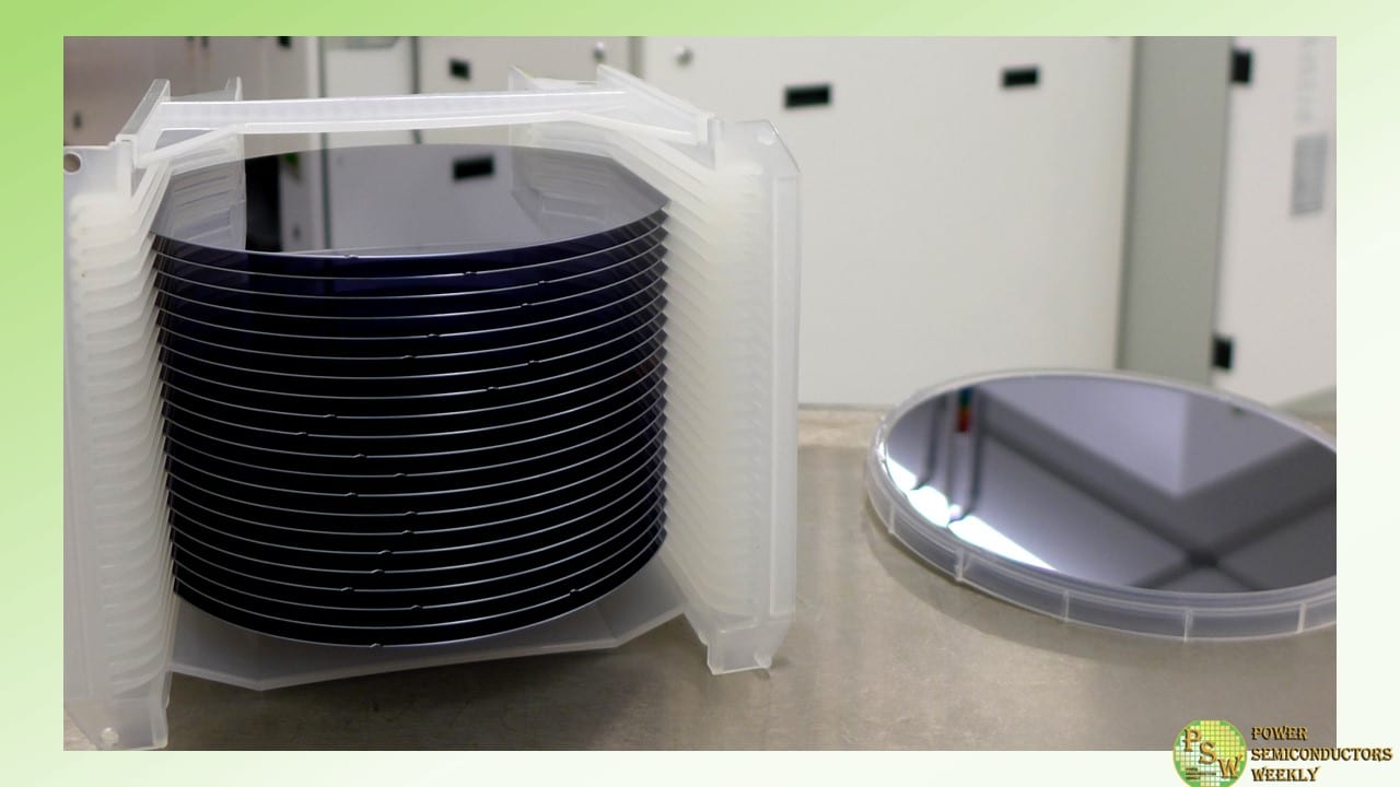
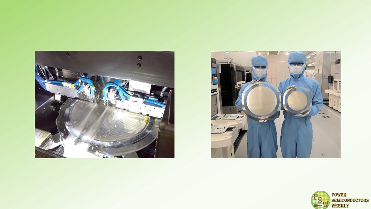
Coherent Corp. announced the launch of its 200 mm silicon carbide epitaxial wafers. Substrate and epi-wafer shipments from the company at 350 micron and 500 micron thickness are now underway.
As a dedicated manufacturer of both SiC substrates and epitaxial wafers, Coherent combines these elements to deliver exceptional quality, performance, and reliability. The new 200 mm SiC epi-wafers are engineered with cutting-edge thickness and doping uniformity, setting new industry standards and supporting the production of superior SiC power semiconductors.
“With our advanced technology, we are not only enhancing the quality of SiC devices but also addressing the growing demand for 200 mm for efficient power-conversion components in critical sectors,” said Gary Ruland, Vice President and General Manager of the SiC Materials Business Unit.
SiC devices are integral to power conversion in electric and hybrid vehicles, energy infrastructure, and high-power EV chargers. The transition from 150 mm to 200 mm diameter wafers responds to the increasing demand for SiC semiconductors, allowing manufacturers to produce more devices per wafer. This shift is expected to enhance productivity and reduce the cost of SiC devices, benefiting a wide range of applications.
By adopting larger wafers, SiC device manufacturers can achieve higher yields and improved cost efficiency because of a 1.8x increase in usable area per wafer. The implementation of state-of-the-art 200 mm tooling brings additional advantages while aligning with the industry’s drive for greater performance and reduced operational costs.
Original – Coherent
-
 LATEST NEWS / PRODUCT & TECHNOLOGY / SiC / WBG
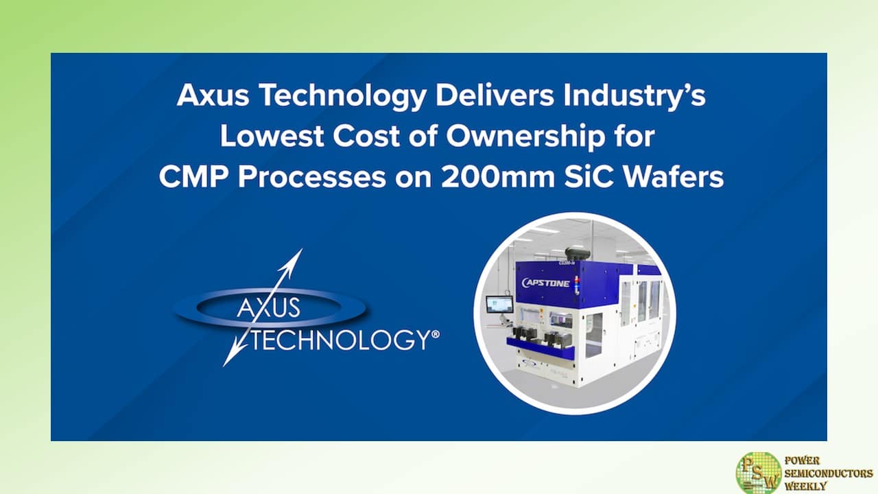
Axus Technology Introduced Industry’s Lowest Cost of Ownership for CMP Processes on 200mm SiC Wafers
September 26, 2024
2 Min ReadAxus Technology, a leading global provider of chemical mechanical planarization (CMP) equipment, critical for semiconductor and compound semiconductor fabrication, announced its flagship CapstoneÆ CS200 platform tools offer the industry’s lowest cost of ownership (CoO) for CMP processes on 200mm silicon carbide (SiC) wafers. Compared to its closest competitor, Axus’s small-footprint Capstone delivers twice the throughput at less than half the total cost per wafer.
Yole Group forecasts the overall SiC manufacturing tool market to top US$4.4 billion by 2029. “The unique properties of SiC require specialized manufacturing tools and lines for processing power SiC devices,” the market analyst firm noted earlier this year. Axus anticipated this need, designing the state-of-the-art Capstone from the ground up to deliver advanced processing capabilities for SiC in power electronics and other applications.
“Many 200mm fabs are looking to upgrade their installed base of CMP tools to products with leading-edge capability and functionality. Our ability to deliver industry-low CoO further underscores our strong market position and capacity to support this shift,” said Axus Technology CEO Dan Trojan. “Capstone features a streamlined workflow and integrated cleaning capability, so it requires half the process steps of older CMP tools. This allows customers to greatly lower their capex investment.”
Key Capstone CoO advantages vs. competitor
- Throughput: 2.5x wafers per hour
- Power consumption: 60% lower
- DI water consumption: 80% lower
- Footprint: 45% smaller
- Capex cost per wafer: 65% lower
- Total cost per wafer: 50% lower
Another factor contributing to Capstone’s lower CoO is its built-in Process Temperature Control (PTC) technology, which enables processing at higher pressures and speeds without exceeding temperature limits of polishing pads and other sensitive components. This feature is vital for SiC and other materials with high hardness and planarization challenges that necessitate more aggressive process conditions.
Axus built its proprietary CoO model using its own system specifications, publicly available specs for competitive tools, actual consumables costs, and real-world performance data supplied by customers. The comprehensive model factors in all CoO contributors: process variables (polish time and removal rates), polishing and cleaning consumables, power and deionized (DI) water usage, system footprint, and equipment capex including cost, utilization and wafer capacity.
Original – Axus Technology
-
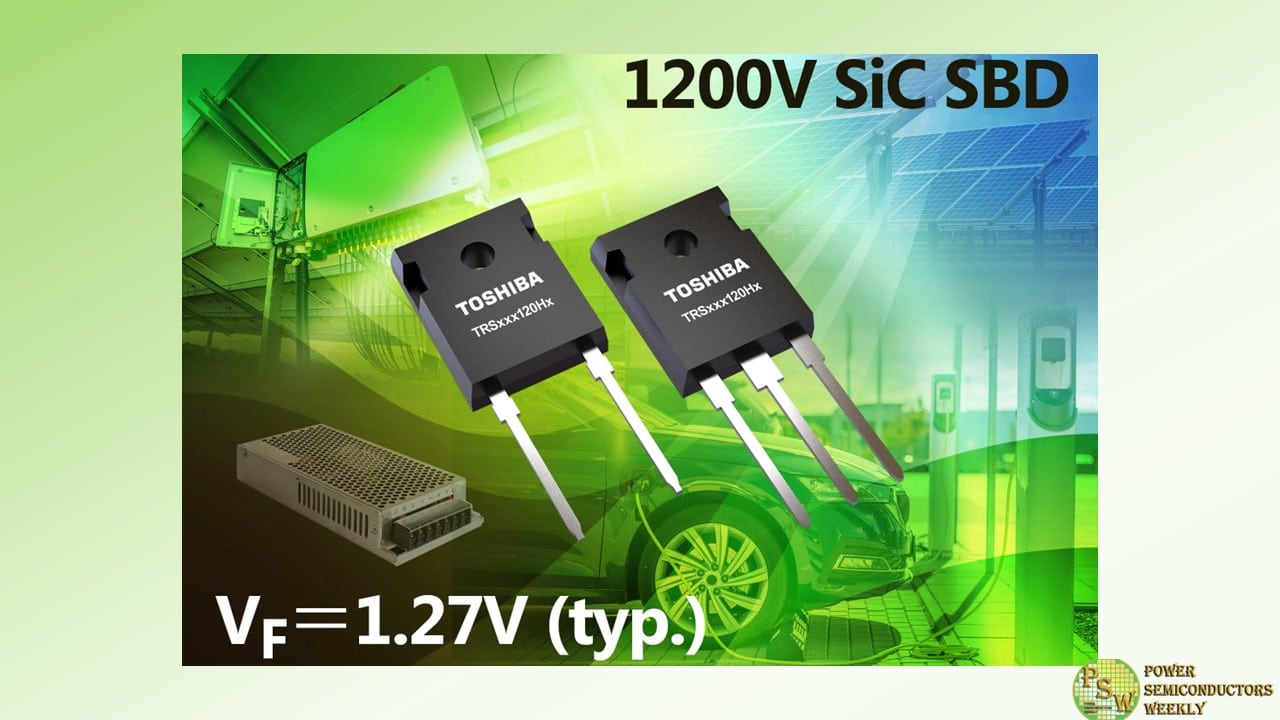
Toshiba Electronics Europe GmbH enhances its silicon carbide (SiC) diode portfolio with ten new 1200V Schottky barrier diodes (SBDs). The TRSxxx120Hx series, comprising five products housed in TO-247-2L packages and five in TO-247 packages, helps designers improve the efficiency of industrial equipment, including photovoltaic (PV) inverters, electric vehicle (EV) charging stations, and switching power supplies.
By implementing an enhanced junction barrier Schottky (JBS) structure, the TRSxxx120Hx series allows a very low forward voltage (VF) of just 1.27V (typ.). The merged PiN-Schottky incorporated into a JBS structure reduces diode losses under high current conditions. The TRS40N120H of the new series accepts a forward DC current (IF(DC)) of 40A (max) and a non-repetitive peak forward surge current (IFSM) of 270A (max), with the maximum case temperature (TC) of all devices being +175°C.
Combined with the lower capacitive charge and leakage current, the products help improve system efficiency and simplify thermal design. For instance, at a reverse voltage (VR) of 1200V, the TRS20H120H diode housed in the TO-247-2L package provides a total capacitive charge (QC) of 109nC and reverse current (IR) of 2µA.
Original – Toshiba
-
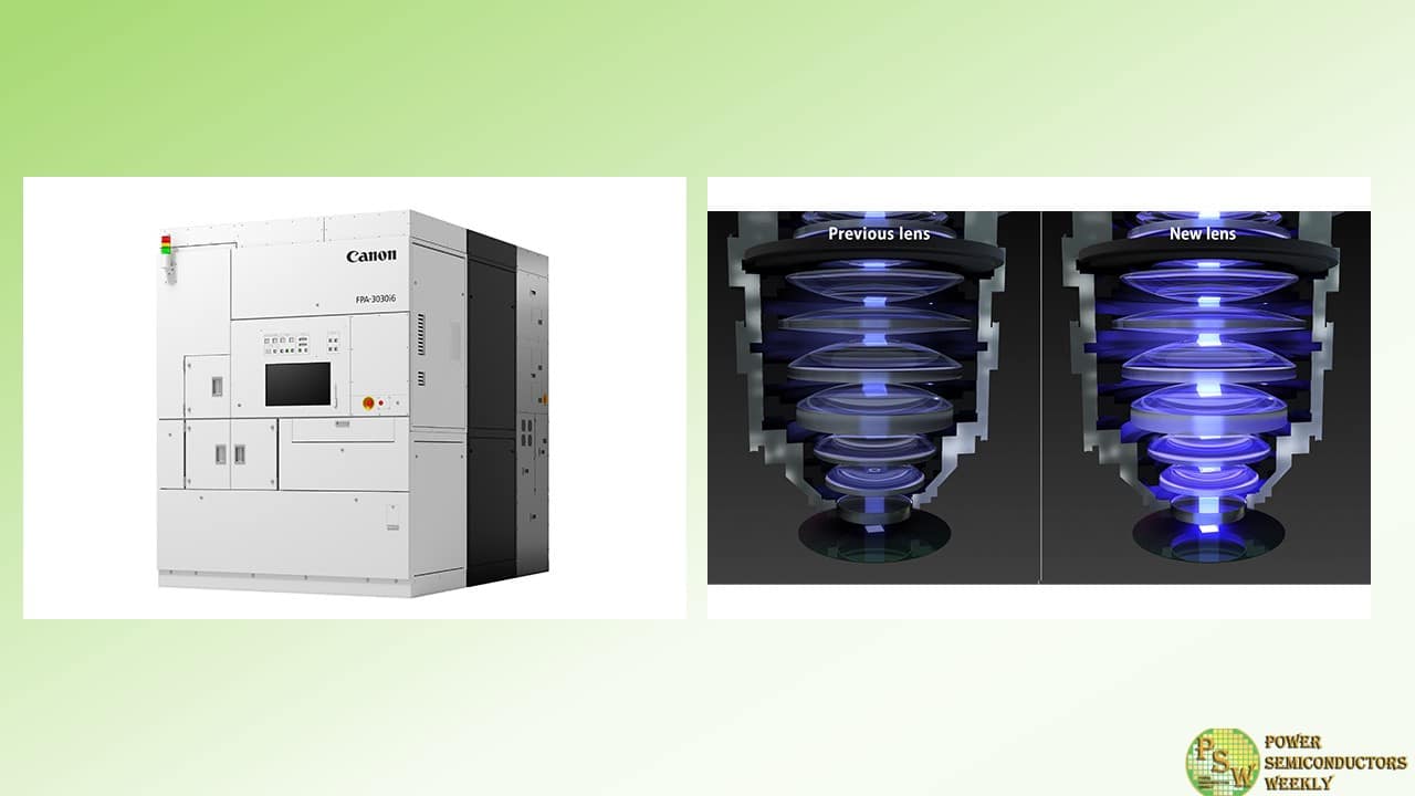
Canon Inc. announced the release of the FPA-3030i6 i-line stepper, a new semiconductor lithography system for processing wafers with a diameter of 8 inches (200 mm) or smaller.
The FPA-3030i6 employs a newly developed projection lens that boasts high transmittance and high-durability. The system reduces lens aberration for high exposure dose processes and improves productivity by shortening exposure time.
The lens is made of high-transmittance glass material that reduces lens aberrations occurring during exposure by more than 50% when compared to previous stepper models. Higher transmittance also helps reduce exposure time while maintaining pattern fidelity, even under high exposure dose conditions.
Improving lens transmittance will also increase exposure intensity and shorten the exposure time required for each process. The FPA-3030i6 standard productivity for 8 inch (200 mm) wafers has increased to 130 wafers per hour from 123 for the previous stepper models.
Additionally, since the lens is highly durable, lens transmittance decrease over time is reduced and productivity can be maintained over the life of the system.
The NA (numerical aperture) range has also been expanded from 0.45~0.63 in the previous model to 0.30~0.63. Allowing for a smaller NA enables customers to select the optimum NA for each device layer.
Optional products including a wafer handling system for special substrates are available for order to meet users’ manufacturing needs for various emerging semiconductor devices including high-power and high-efficiency green devices.
The FPA-3030i6 is designed to support a wider range of device fabrication thanks to a variety of available process options for silicon (Si) as well as sapphire and compound semiconductor materials such as silicon carbide (SiC), gallium nitride (GaN) and gallium arsenide (GaAs) substrates.
Canon will offer wafer feeding options enabling handling of substrates from 2 inches (50 mm) to 8 inches (200 mm) in diameter, as well as thick, thin and warped substrate handling.
Original – Canon
-
STMicroelectronics introduced its fourth generation STPOWER silicon carbide (SiC) MOSFET technology. The Generation 4 technology brings new benchmarks in power efficiency, power density and robustness. While serving the needs of both the automotive and industrial markets, the new technology is particularly optimized for traction inverters, the key component of electric vehicle (EV) powertrains. The company plans to introduce further advanced SiC technology innovations through 2027 as a commitment to innovation.
“STMicroelectronics is committed to driving the future of electric mobility and industrial efficiency through our cutting-edge silicon carbide technology. We continue to advance SiC MOSFET technology with innovations in the device, advanced packages, and power modules,” said Marco Cassis, President, Analog, Power & Discrete, MEMS and Sensors Group. “Together with our vertically integrated manufacturing strategy, we are delivering industry leading SiC technology performance and a resilient supply chain to meet the growing needs of our customers and contribute to a more sustainable future.”
As the market leader in SiC power MOSFETs, ST is driving further innovation to exploit SiC’s higher efficiency and greater power density compared to silicon devices. This latest generation of SiC devices is conceived to benefit future EV traction inverter platforms, with further advances in size and energy-saving potential. While the EV market continues to grow, challenges remain to achieve widespread adoption and car makers are looking to deliver more affordable electric cars.
800V EV bus drive systems based on SiC have enabled faster charging and reduced EV weight, allowing car makers to produce vehicles with longer driving ranges for premium models. ST’s new SiC MOSFET devices, which will be made available in 750V and 1200V classes, will improve energy efficiency and performance of both 400V and 800V EV bus traction inverters, bringing the advantages of SiC to mid-size and compact EVs — key segments to help achieve mass market adoption.
The new generation SiC technology is also suitable for a variety of high-power industrial applications, including solar inverters, energy storage solutions and datacenters, significantly improving energy efficiency for these growing applications.
ST has completed qualification of the 750V class of the fourth generation SiC technology platform and expects to complete qualification of the 1200V class in the first quarter of 2025. Commercial availability of devices with nominal voltage ratings of 750V and 1200V will follow, allowing designers to address applications operating from standard AC-line voltages up to high-voltage EV batteries and chargers.
ST’s Generation 4 SiC MOSFETs provide higher efficiency, smaller components, reduced weight, and extended driving range compared to silicon-based solutions. These benefits are critical for achieving widespread adoption of EVs and leading EV manufacturers are engaged with ST to introduce the Generation 4 SiC technology into their vehicles, enhancing performance and energy efficiency. While the primary application is EV traction inverters, ST’s Generation 4 SiC MOSFETs are also suitable for use in high-power industrial motor drives, benefiting from the devices’ improved switching performance and robustness.
This results in more efficient and reliable motor control, reducing energy consumption and operational costs in industrial settings. In renewable energy applications, the Generation 4 SiC MOSFETs enhance the efficiency of solar inverters and energy storage systems, contributing to more sustainable and cost-effective energy solutions. Additionally, these SiC MOSFETs can be utilized in power supply units for server datacenters for AI, where their high efficiency and compact size are crucial for the significant power demands and thermal management challenges.
To accelerate the development of SiC power devices through its vertically integrated manufacturing strategy, ST is developing multiple SiC technology innovations in parallel to advance power device technologies over the next three years. The fifth generation of ST SiC power devices will feature an innovative high-power density technology based on planar structure. ST is at the same time developing a radical innovation that promises outstanding on-resistance RDS(on) value at high temperatures and further RDS(on) reduction, compared to existing SiC technologies.
ST will attend ICSCRM 2024, the annual scientific and industry conference exploring the newest achievements in SiC and other wide bandgap semiconductors. The event, from September 29 to October 04, 2024, in Raleigh, North Carolina will include ST technical presentations and an industrial keynote on ‘High volume industrial environment for leading edge technologies in SiC’.
Original – STMicroelectronics
-

Vishay Intertechnology, Inc. announced that it is implementing restructuring actions designed to optimize the Company’s manufacturing footprint and streamline business decision making as it executes its Vishay 3.0 growth strategy.
The restructuring actions will be implemented in phases and include:
- Selling, general, and administrative functions will be streamlined beginning immediately and through 4Q 2025, resulting in severance payments to approximately 170 employees, or 6% of the SG&A workforce.
- The closure of three manufacturing facilities. A Diodes segment back-end facility in Shanghai, China is expected to be closed by the end of 2026 with production transfers completed in phases beginning 4Q 2025. In addition, two small facilities in the Resistors segment in Fichtelberg, Germany, and in Milwaukee, Wisconsin, are expected to be closed in 2026. As a result of these facility closures, Vishay will reduce its direct labor by approximately 365 employees, or 2% of its total manufacturing labor workforce.
- Various changes in manufacturing operations and production transfers, which will result in severance payments to approximately 260 employees.
The Company expects to incur pre-tax cash charges of approximately $38 to $42 million, primarily related to severance costs, as a result of these programs, mostly in 3Q 2024. Once the program is fully implemented by the end of 2026, Vishay expects to realize annualized cost savings of at least $23 million of which approximately $12 million is expected to be in selling, general and administration expenses. The Company expects to realize immediate annualized cost savings of approximately $9 million. Beginning 1Q 2025, the Company expects to realize approximately $12 million in annualized cost savings.
“As we implement Vishay 3.0, reshaping the Company and preparing for our next phase of growth, we continuously task ourselves with identifying opportunities to best foster a business minded approach to decision making, further enhance our customer first focus and improve cost efficiencies,” said Joel Smejkal, Vishay’s President and Chief Executive Officer.
“With that in mind, we are undertaking these restructuring actions in part to eliminate barriers to execution and to intensify the sense of urgency. We’re also taking our first step to optimize our global manufacturing footprint, closing smaller single product line facilities and moving toward campus manufacturing structures with multiple product lines. Collectively, these actions will help us execute our five-year growth strategy to accelerate our revenue growth rate, expand profitability and drive higher returns.”
The Company’s estimates of the costs related to its cost reduction programs and anticipated annual savings represent its current best estimates. However, such estimates are preliminary and subject to change as the Company implements these programs.
Original – Vishay Intertechnology
-

Polar Semiconductor announced that the company has completed its sale to Niobrara Capital and Prysm Capital. The $175 Million in equity financing has been closed to convert Polar to a U.S.-owned merchant foundry and fund expansion of its Bloomington, Minnesota manufacturing facility. In total, Polar expects to invest approximately $525 Million in the expansion of the facility over the next two years and branch into innovative technologies to serve new customers and markets.
Polar has signed Award Documents with the U.S. Department of Commerce, under which it will receive up to $123 Million in direct funding as part of the U.S. CHIPS and Science Act, and with the Minnesota Department of Employment and Economic Development (DEED), under which it will receive $75 Million in incentives as part of the Minnesota Forward Fund. Polar is the first award recipient under the CHIPS Incentives Program’s Funding Opportunity for Commercial Fabrication Facilities and the Minnesota Forward Fund. Polar plans to claim the Department of the Treasury’s Investment Tax Credit, which is expected to be up to 25% of qualified capital expenditures.
Through these investments, Polar plans to:
- Double production capacity, ramping up from approximately 20,000 wafers per month to nearly 40,000 wafers per month,
- Upgrade and modernize its facility to become globally competitive through economies of scale,
- Deliver cutting-edge semiconductor solutions to the U.S. automotive, aerospace, defense, optoelectronics, MEMS, and medical device industries, and
- Create 160+ new jobs, strengthening Polar’s commitment to its community and driving economic growth in the State.
“Semiconductors – those tiny chips smaller than the tip of your finger – power everything from smartphones to cars to satellites and weapons systems. I signed the CHIPS and Science Act to revitalize American leadership in semiconductors, strengthen our supply chains, protect our national security, and advance American competitiveness. And over the last three and a half years, we have done just that, catalyzing over $400 billion in private sector investments in semiconductors and electronics that are creating over 115,000 construction and manufacturing jobs. This year alone, the United States is on pace to see more investment in electronics manufacturing construction than it did over the last 24 years combined,” said President Joe Biden.
“Today’s announcement that the Department of Commerce has finalized the first commercial CHIPS Incentives award with Polar Semiconductor marks the next phase of the implementation of the CHIPS and Science Act and demonstrates how we continue to deliver on the Investing in America agenda. Polar’s new facility will also be completed under a Project Labor Agreement to support its construction workforce, creating good-quality union jobs in Bloomington, Minnesota. Today’s announcement is just one of the many ways our Investing in America agenda is reshoring U.S. manufacturing, investing in workers and communities across the country, and advancing America’s leadership in the technologies of tomorrow.”
“Today represents an important milestone in the implementation of the historic CHIPS and Science Act as we announce the first award agreement with Polar,” said U.S. Secretary of Commerce Gina Raimondo. “The Biden-Harris Administration’s investment in Polar will create a new U.S.-owned foundry for sensor and power semiconductors and modernize and expand Polar’s facilities in Minnesota, strengthening our national and economic security, bolstering our supply chains, and creating quality jobs.”
“America must stay on the cutting edge of manufacturing to maintain our economic edge on the world stage. This landmark federal investment in Polar Semiconductor’s Bloomington facility is a major step toward strengthening domestic production of advanced semiconductors,” said Senator Amy Klobuchar. “I worked closely with Polar Semiconductor to secure this grant and ensure Minnesota continues to be a premier destination for business investment.”
“Minnesota is lucky to be home to businesses like Polar that consistently produce innovative, high-quality products with a global reach,” said Governor Tim Walz. “With partnerships like this, we can lead the nation in creating high-growth, high-demand, good-paying jobs.”
Surya Iyer, President and COO of Polar Semiconductor said, “Polar and its employees are excited to embark on our transformative project. We welcome new customers and partnerships, and as a domestic U.S.-owned sensor and advanced power semiconductor merchant foundry, we will support technology and design innovation, protect intellectual property, facilitate onshoring and technology transfers, and provide efficient low- to high-volume manufacturing with world-class quality. Through our collaborative and sustained workforce development efforts, we expect to support customers with highly skilled employees today and into the future. We are pleased to close on the significant equity investment from Niobrara Capital and Prysm Capital, and we extend our sincere thanks to our partners at the U.S. Department of Commerce, the State of Minnesota, and the City of Bloomington for their support of the future of American semiconductor manufacturing.”
Chip Schorr, Founder and Managing Partner of Niobrara Capital, said, “Polar is positioned to enable many of America’s most critical industries, such as aerospace and defense, automotive and medical, to have a dedicated, high performance, low cost, onshore source of power semiconductors and sensors. We are pleased to be partnering with the company to support its growth and the growth of U.S. technology manufacturing leadership.”
Jay Park, Co-Founder and Managing Partner of Prysm Capital, said “The public and private investment in Polar is a testament to the strength of Polar’s offering and team and a significant event for onshore technology investment in America. We are already seeing robust demand for Polar’s planned capacity that exceeds our expectations and reinforces our confidence in Polar.”
Polar Semiconductor leads the Minnesota CHIPS Coalition, which is composed of more than 70 organizations, including manufacturers, supply-chain partners, education and training providers, labor organizations, and state and local governments. The coalition is determined to reinvigorate the region’s legacy in technology and establish the Midwest’s semiconductor industry as a national leader.
Polar also leads the Minnesota CHIPS Coalition Workforce Partnership, collaborating with semiconductor companies, educational institutions, training organizations, the Governor’s Workforce Development Board (GWDB), and DEED. The goal is to develop a next-generation high-tech manufacturing workforce through training, upskilling, and apprenticeships. These efforts are supported by state investments and a $3 Million dedicated portion of the CHIPS award. The partnership will also draw on national programs, like Indiana’s DoD-backed SCALE initiative, to enhance local efforts.
Original – Polar Semiconductor
-
Resonac Corporation (formerly Showa Denko K.K.) and Soitec have signed an agreement to develop 200mm (8-inch) SmartSiC™ silicon carbide (SiC) wafers using Resonac substrates and epitaxy processes, in a major step for the deployment of Soitec’s high-yielding silicon carbide technology in Japan and other international markets.
SmartSiC™ silicon carbide is a disruptive compound semiconductor material providing superior performance and efficiency over silicon in high-growth power applications for electric mobility and industrial processes. It allows for more efficient power conversion, lighter and more compact designs and overall system cost savings – all key factors for success in automotive and industrial systems.
Christophe Maleville, Chief Technology Officer at Soitec, commented: “Silicon carbide is beingadopted for EV and industrial applications, where it brings a significant system cost advantage. To further accelerate this adoption, silicon carbide yield and productivity must be improved. Associating Resonac premium quality SiC materials with Soitec’s unique 200mm (8-inch) SmartSiC™ technology will support volume availability of record quality epi-ready substrate. The combination of our respective technologies and products will optimize these substrates using Resonac’s high-quality epitaxy. Soitec is proud and excited to be partnering with Resonac to develop a best-in-class combined SiC product offering for Japan and the world.”
Makoto Takeda, General Manager of Device Solutions Business Unit at Resonac, commented: “We are delighted to announce this partnership with Soitec, which is fully aligned with our broader commitment to sustainable and energy-efficient semiconductor solutions. By combining Resonac’s high quality monocrystalline silicon carbide wafers with Soitec’s unique SmartSiC™ technology, we will deliver improved production efficiency of 200mm (8-inch) silicon carbide wafers and diversify the epi-wafer supply chain.”
Soitec’s SmartSiC™ silicon carbide wafers, or engineered substrates, are produced using the company’s proprietary SmartCut™ technology to bond an ultra-fine layer of high-quality monoSiC ‘donor’ wafer to a low-resistivity polycrystalline (poly-SiC) ‘handle’ wafer. The resulting engineered substrate delivers significantly improved device performance and manufacturing yields. By allowing multiple re-uses of the prime quality mono-SiC wafer, the process also reduces overall energy consumption during wafer manufacturing.
Soitec has a new fabrication plant at its headquarters in Bernin, France, primarily dedicated to the production of SmartSiC™ wafers for electric vehicles, renewable energy and industrial equipment component applications.
Original – Soitec
