-

Vanguard International Semiconductor Corporation and NXP Semiconductors N.V. announced that they have obtained all necessary approvals from relevant authorities and injected capital to officially establish the VisionPower Semiconductor Manufacturing Company Pte Ltd (VSMC) joint venture. The company will now proceed with the planned construction of VSMC’s first 300mm wafer manufacturing facility.
VIS and NXP announced on June 5 this year plans to establish the VSMC joint venture in Singapore to build a 300mm wafer fab with a total investment of approximately $7.8 billion.
“We express our gratitude to the governments and regulatory authorities of Taiwan, Singapore, and other countries for their strong support, which enabled us to obtain the necessary approvals and proceed with this significant investment as scheduled. VSMC’s first 300mm fab is a concrete manifestation of VIS’ commitment to meeting customer demands, expanding our manufacturing capacity, and diversifying our global manufacturing bases.”VIS Chairman Leuh Fang
“We thank all the relevant government agencies for moving with speed to support the VSMC joint venture project. The VSMC fab perfectly aligns with our hybrid manufacturing strategy and helps ensure we have a manufacturing base which delivers competitive cost, supply control and geographic resilience to support our long-term growth objectives.”NXP President and CEO Kurt Sievers
VSMC will begin construction on its initial phase of the wafer fab in the second half of this year, with initial production slated to begin in 2027. Upon the successful ramp of the initial phase, a second phase will be considered and developed pending commitments by VIS and NXP.
The 300mm fab will support 130nm to 40nm mixed-signal, power management and analog products, targeting the automotive, industrial, consumer and mobile end markets. The related technology license and technology transfer will be from TSMC, and a Technology License Agreement with TSMC has been signed.
With an expected output of 55,000 300mm wafers per month in 2029, the joint venture will create approximately 1,500 jobs while contributing to the development of the upstream and downstream supply chains, contributing to Singapore and the global semiconductor ecosystem.
Original – NXP Semiconductors
-

Littelfuse, Inc. announced the launch of the IX4341 and IX4342 dual 5 ampere low-side MOSFET gate drivers. These gate drivers are specifically designed for driving MOSFETs and complete the existing IX434x driver series by adding the remaining two logic input versions. The IX434x series now consists of dual non-inverting, dual inverting, and non-inverting and inverting input versions, providing customers with a comprehensive range of options.
The IX4341 and IX4342 drivers’ short propagation delay times of 16 nanoseconds and brief rise and fall times of 7 nanoseconds make them ideal for high-frequency applications. Additionally, for higher current requirements, electronics designers can parallel the two channels of the IX4340 and IX4341 devices to form a single 10 A driver, providing flexibility and scalability.
A notable feature of the IX434x drivers is their compatibility with TTL and CMOS logic inputs, enabling direct interfacing with most controllers. Furthermore, each output has an independent ENABLE function and under-voltage lockout circuitry (UVLO) to ensure reliable and safe operation. In case of eventual insufficient supply voltage, the gate driver output is asserted low, turning the external power device off.
The IX4341 and IX4342 dual 5 A low-side gate drivers find applications in various markets, including:
- general industrial and electrical equipment,
- appliances,
- building solutions,
- data centers,
- energy storage, and
- renewable energy.
These low-side MOSFET gate drivers are ideally suited for numerous industrial applications such as:
- switch-mode power supplies,
- DC-DC converters,
- motor controllers, and
- power converters.
The IX434x devices are available in standard 8-pin SOIC, thermally enhanced 8-pin SOIC, and 3×3 mm² MSOP packages, offering customers a range of options to suit their specific needs.
“This new series of dual five-ampere low-side gate drivers simplify circuit design with its high level of integration and compatibility with various logic input versions,” said June Zhang, Product Manager, Integrated Circuits Division, Semiconductor Business Unit, at Littelfuse. “With these drivers, customers can expect enhanced performance and protection for their power devices.”
The IX434x dual 5 A low-side gate drivers find applications in various industries, including general industrial and electrical equipment, appliances, building solutions, data centers, energy storage, and renewable energy.
They serve as a direct drop-in alternative to similar available drivers, providing customers with industry-standard options to meet their supply demands.
Original – Littelfuse
-

Navitas Semiconductor announced the release of a portfolio of third-generation automotive-qualified SiC MOSFETs in D2PAK-7L (TO-263-7) and TOLL (TO-Leadless) surface-mount (SMT) packages.
Navitas’ proprietary ‘trench-assisted planar’ technology provides world-leading performance over temperature and delivers high-speed, cool-running operation for electric vehicle (EV) charging, traction, and DC-DC conversion. With case temperatures up to 25°C lower than conventional devices, Gen-3 Fast SiC offers an operating life up to 3x longer than alternative SiC products, for high-stress EV environments.
Gen-3 Fast MOSFETs are optimized for the fastest switching speed, highest efficiency, and support increased power density in EV applications such as AC compressors, cabin heaters, DC-DC converters, and on-board chargers (OBCs). Navitas’ dedicated EV Design Center has demonstrated leading edge OBC system solutions up to 22 kW with 3.5 kW/liter power density, and over 95.5% efficiency.
400 V-rated EV battery architectures are served by the new 650 V Gen-3 Fast MOSFETs featuring RDS(ON) ratings from 20 to 55 mΩ. The 1,200 V ranges from 18 to 135 mΩ and is optimized for 800 V systems.
Both 650 and 1,200 V ranges are AEC Q101-qualified in the traditional SMT D2PAK-7L (TO-263-7) package. For 400 V EVs, the 650 V-rated, surface-mount TOLL package offers a 9% reduction in junction-to-case thermal resistance (RTH,J-C), 30% smaller PCB footprint, 50% lower height, and 60% smaller size than the D2PAK-7L. This enables very high-power density solutions, while minimal package inductance of only 2 nH ensures excellent fast-switching performance and lowest dynamic package losses.
The automotive-qualified 650 V and 1200 V G3F SiC MOSFET family in D2PAK-7L and TOLL surface mount packages are released and available immediately for purchase.
Original – Navitas Semiconductor
-

Axcelis Technologies, Inc. will be a top-level Platinum Sponsor at the International Conference on Ion Implantation Technology 2024 (IIT 2024) taking place September 23-26 at the Toyama International Conference Center in Japan.
IIT 2024 is the 24th Conference in the biennial series focused on the major challenges in current and emerging technologies related to implant/doping and annealing processes, device applications, equipment, metrology and modeling.
At the event, Axcelis will host a company exhibit and the company’s technologists and collaborators will present on nine topics:
- Performance of an Aluminum Sputtering Source for High Current Doping in Power Devices
- Energetic and Surface Metals Characterization of Purion XEmax With and Without Boost™ Technology Using Vapor Phase Decomposition-Inductively Coupled Plasma Mass Spectrometry
- Radiation Characterization and Mitigation of High Energy H+ Beams
- Wear-Resistant Surface Coatings for Long Electrostatic Chuck Life and Stable Performance
- Self-contained Predictive System Diagnostic Sensors
- Comparison of Arsenic and Antimony Dopant Distribution Profiles of Very High Energy Implantations
- New Challenges and Opportunities in Wide Bandgap Materials with Ion Implantation and Annealing Co-Optimization
- Dual Cathode Ion Source for Axcelis’ High Energy Implanters
- Low Metals Ion Source
President and CEO of Axcelis Technologies Russell Low said, “We’re excited to be a Platinum Sponsor of IIT 2024, one of the most important technology forums in the ion implantation industry. We’re especially pleased to be participating at the event in Japan this year, which is a very important market for Axcelis. Axcelis recently opened several new Service Centers in Japan to support our expanding customer base. We remain focused on growing our global market share by providing customers the most innovative, enabling implant technology and support solutions to ensure their success.”
For more information on the event, or to register, visit the conference website at https://smartconf.jp/content/iit2024.
Original – Axcelis Technologies
-
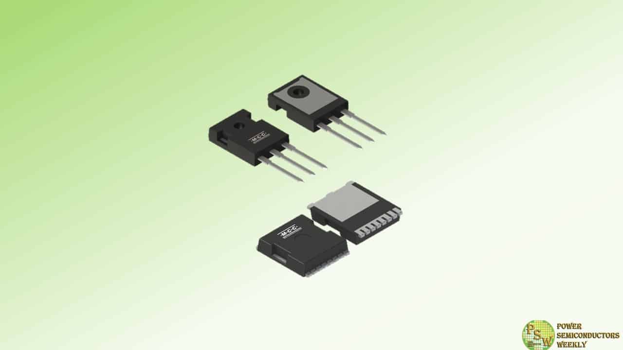
MCC Semi rolled out three new 600V MOSFETs that go beyond high performance. Designed with an integrated fast recovery diode, these advanced components help solve the challenges engineers face when trying to maximize efficiency while minimizing power losses and heat generation.
Ideal for high-voltage applications, MSJWFR60N60, MCTK075N60FH, and MCTK105N60FH feature on-resistance in the sub-100mΩ range — with options as low as 30mΩ — to significantly reduce conduction losses and ensure efficient power delivery.
A low gate charge only adds to their excellence, especially in high-frequency applications where response times are critical. Available in a through-hole TO-247 package and space-saving SMD TOLL-8L options with a Kelvin source connection, these MOSFETs offer a versatile solution for enhancing overall system performance.
Improve reliability for various applications, such as power supplies, AC-DC converters, motor drives, and renewable energy systems, with these low RDS(on) semiconductors from MCC.
Features & Benefits:
- Superjunction MOSFET technology: Enhances efficiency and reduces power losses
- Low on-resistance: Minimizes conduction losses for improved performance
- Low conduction losses: Ensures greater efficiency in power applications
- Low gate charge: Facilitates faster switching and reduced energy consumption
- Integrated fast recovery diode: Provides rapid recovery for better switching performance
- High-speed switching: Supports high-frequency operations, perfect for modern applications
- Versatile packages: Enables design flexibility with through-hole (TO-247) and SMD with Kelvin Source (TOLL-8L-KS) options
Original – Micro Commercial Components
-
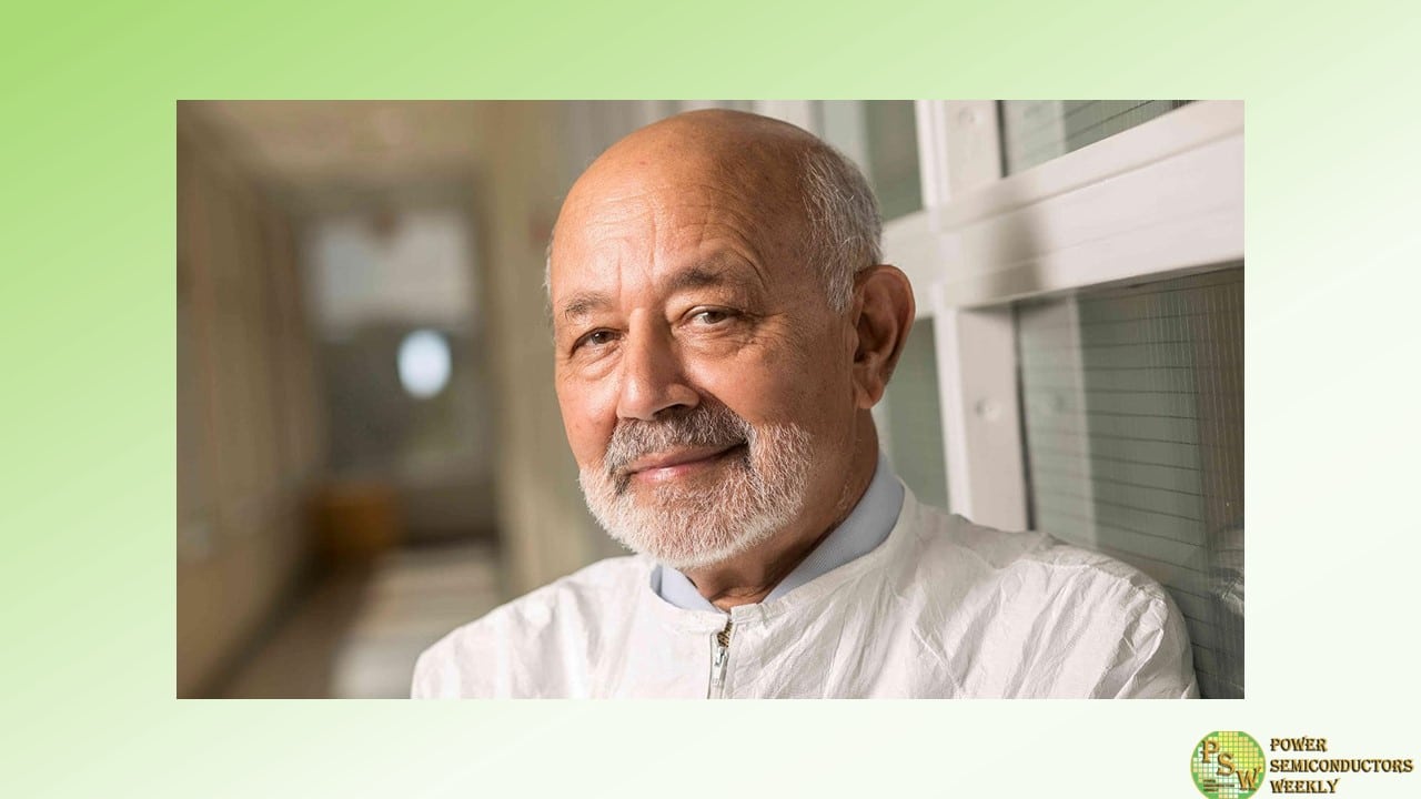
North Carolina State University Professor B. Jayant Baliga has been awarded the 2024 Millennium Technology Prize for his work on the invention, development and commercialization of insulated gate bipolar transistors (IGBTs), which play a critical role in energy efficiency for technologies worldwide. The Millennium Technology Prize, which comes with a €1 million award, is the most prestigious international award focused on recognizing technological innovation.
The IGBT is an energy-saving semiconductor switch that controls the flow of power from an electrical energy source to any application that needs energy. The IGBT improves energy efficiency by more than 40 percent in an array of products, from cars and refrigerators to light bulbs, and is a critical component enabling modern compact cardiac defibrillators.
The IGBT has reduced global carbon dioxide emissions by over 82 gigatons (180 trillion pounds) over the past 30 years. This is equivalent to offsetting carbon dioxide emissions from all human activity for three years, based on average emissions of the past 30 years.
“The IGBT has already had and continues to have a major impact on supporting sustainability with improved living standards worldwide, while mitigating environmental impact,” says Minna Palmroth, chair of the Board of Technology Academy Finland, the foundation which awards the Millennium Technology Prize. “The main solution to tackle global warming is electrification and moving to renewable energy. The IGBT is the key enabling technology in addressing these issues.”
“It is very exciting to have been selected for this great honor,” says Baliga, who is the Progress Energy Distinguished University Emeritus Professor of Electrical and Computer Engineering at NC State.
“I am particularly happy that the Millennium Technology Prize will bring attention to my innovation, as the IGBT is an embedded technology that is hidden from the eyes of society. It has enabled a vast array of products that have improved the comfort, convenience and health of billions of people around the world while reducing carbon dioxide emissions to mitigate global warming. Informing the public of this impactful innovation will illustrate the betterment of humanity by modern technology.”
Baliga’s portfolio of 123 U.S. patents includes many other inventions that have also been commercialized. The split-gate power MOSFET is widely manufactured for use in laptops, PCs and servers. And his silicon carbide inventions – including the JBS rectifier and shielded channel power MOSFET – are used in a variety of state-of-the-art electrical power management technologies.
Baliga – who Forbes has called “the man with the world’s largest negative carbon footprint” – continues to work on technological challenges related to energy efficiency. He and his collaborators are currently working on new inventions to improve efficiencies related to solar power generation, electric vehicles and power delivery for AI servers.
The Millennium Technology Prize will be presented to Professor Bantval Jayant Baliga in Finland on Oct. 30 in an award ceremony that also celebrates the 20th anniversary of the prize. The prize will be presented by its patron, the president of Finland.
The €1 million Millennium Technology Prize is the preeminent award focused on technological innovations for a better life. This includes work that improves human well-being, biodiversity and wider sustainability. Overseen by the Technology Academy Finland, it was first awarded in 2004, and its patron is the President of Finland. Winners are selected by a distinguished international panel of experts from academia and industry. Innovations must be backed up by rigorous academic and scientific research and fulfill several criteria, including promoting sustainable development and biodiversity, having generated applications with commercial viability, and creating accessible socio-economic value.
Past winning innovations range from DNA sequencing that helped to develop COVID-19 vaccines, to ethical stem-cell research and versatile, affordable smart technology. Visit the Millennium Prize website for more information.
Original – North Carolina State University
