-
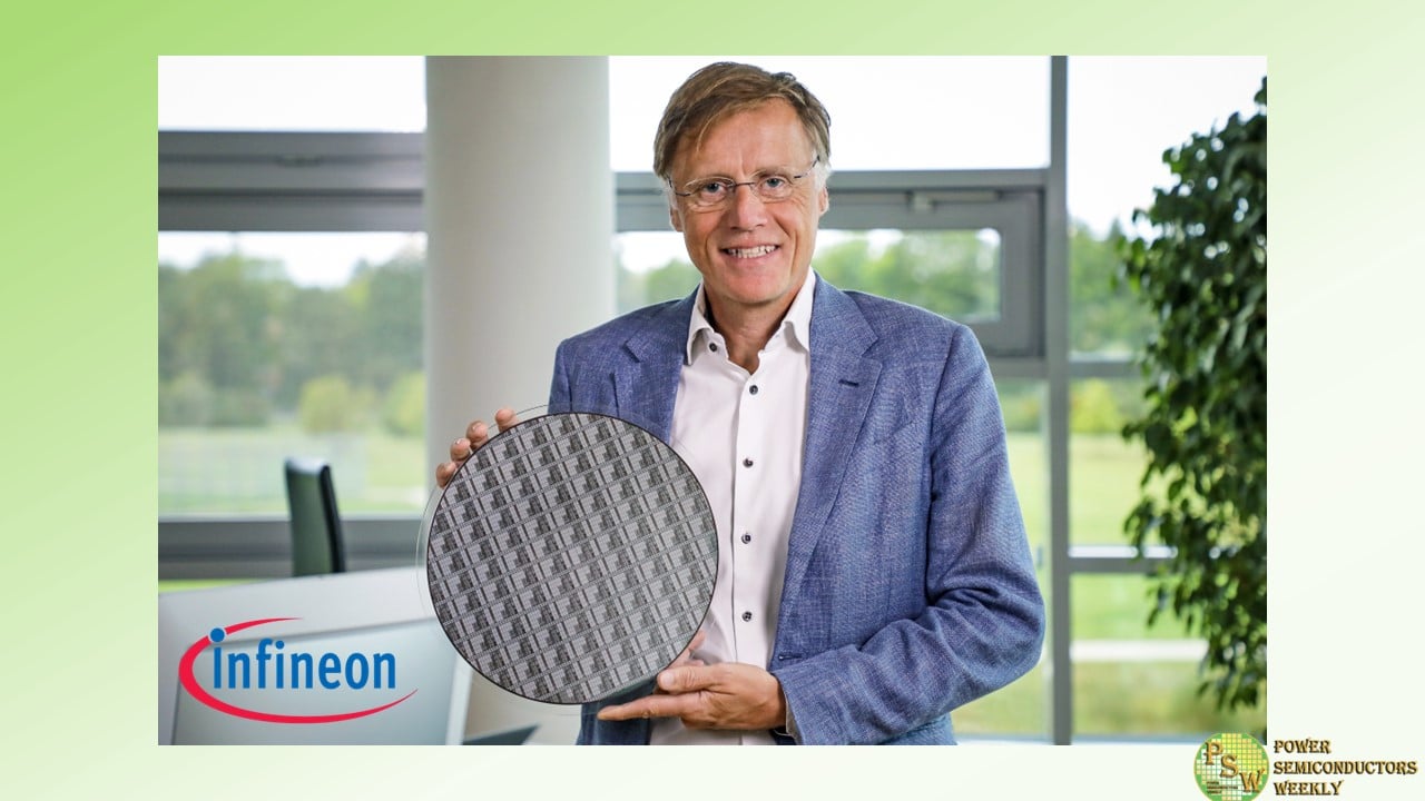
Infineon Technologies AG announced that the company has succeeded in developing the world’s first 300 mm power gallium nitride (GaN) wafer technology. Infineon is the first company in the world to master this groundbreaking technology in an existing and scalable high-volume manufacturing environment. The breakthrough will help substantially drive the market for GaN-based power semiconductors.
Chip production on 300 mm wafers is technologically more advanced and significantly more efficient compared to 200 mm wafers, since the bigger wafer diameter fits 2.3 times as many chips per wafer.
GaN-based power semiconductors find fast adoption in industrial, automotive, and consumer, computing & communication applications, including power supplies for AI systems, solar inverters, chargers and adapters, and motor-control systems. State-of-the art GaN manufacturing processes lead to improved device performance resulting in benefits in end customers’ applications as it enables efficiency performance, smaller size, lighter weight, and lower overall cost. Furthermore, 300 mm manufacturing ensures superior customer supply stability through scalability.
“This remarkable success is the result of our innovative strength and the dedicated work of our global team to demonstrate our position as the innovation leader in GaN and power systems,” said Jochen Hanebeck, CEO of Infineon Technologies AG. “The technological breakthrough will be an industry game-changer and enable us to unlock the full potential of gallium nitride. Nearly one year after the acquisition of GaN Systems, we are demonstrating again that we are determined to be a leader in the fast-growing GaN market. As a leader in power systems, Infineon is mastering all three relevant materials: silicon, silicon carbide and gallium nitride.”
Infineon has succeeded in manufacturing 300 mm GaN wafers on an integrated pilot line in existing 300 mm silicon production in its power fab in Villach (Austria). The company is leveraging well-established competence in the existing production of 300 mm silicon and 200 mm GaN. Infineon will further scale GaN capacity aligned with market needs. 300 mm GaN manufacturing will put Infineon in a position to shape the growing GaN market which is estimated to reach several billion US-Dollars by the end of the decade.
This pioneering technological success underlines Infineon’s position as a global semiconductor leader in power systems and IoT. Infineon is implementing 300 mm GaN to strengthen existing and enabling new solutions and application fields with an increasingly cost-effective value proposition and the ability to address the full range of customer systems. Infineon will present the first 300 mm GaN wafers to the public at the electronica trade show in November 2024 in Munich.
A significant advantage of 300 mm GaN technology is that it can utilize existing 300 mm silicon manufacturing equipment, since gallium nitride and silicon are very similar in manufacturing processes. Infineon’s existing high-volume silicon 300 mm production lines are ideal to pilot reliable GaN technology, allowing accelerated implementation and efficient use of capital. Fully scaled 300 mm GaN production will contribute to GaN cost parity with silicon on R DS(on) level, which means cost parity for comparable Si and GaN products.
300 mm GaN is another milestone in Infineon’s strategic innovation leadership and supports Infineon’s mission of decarbonization and digitalization.
Original – Infineon Technologies
-
Infineon Technologies AG has been nominated for the Deutscher Zukunftspreis 2024, the Federal President’s Award for Technology and Innovation, for its development of a new type of energy-saving chip based on the innovative semiconductor material silicon carbide (SiC). The Jury of Deutscher Zukunftspreis has announced the three nominated teams in Munich.
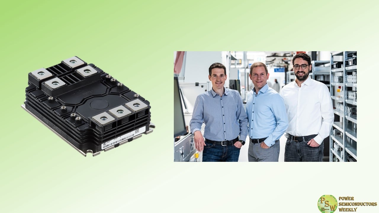
A team of developers from Infineon, together with Chemnitz University of Technology, has succeeded in developing the world’s first silicon carbide MOSFET with a vertical channel (trench MOSFET) and innovative copper contacting in the 3300V voltage class. The new SiC modules and the power converters equipped with the modules represent a revolutionary innovation leap in semiconductor technology from conventional silicon to more energy-efficient silicon carbide, which reduces switching losses in high-current applications by 90%.
MOSFETs are electrical switches for a wide range of applications. Trench MOSFETs differ from so-called planar MOSFETs in their cell structure and performance. While the current flow in planar MOSFETs is initially horizontal, trench MOSFETs offer purely vertical channels. This results in a higher cell density per surface area, which in turn significantly reduces the losses in the chip during energy conversion and therefore increases efficiency.
“The transition towards green energy and many other pressing challenges of our time can only be solved with technological progress,” said Jochen Hanebeck, CEO of Infineon Technologies AG. “It is therefore important to promote and reward innovation and make it visible in society. The ‘Deutscher Zukunftspreis’ is the most important national award that is presented with this aim in mind. The nomination is a great honor for us and proof of the successful research and development work at Infineon. Congratulations to all colleagues involved!”
The CoolSiC™ XHP™2 module family enables significant energy savings, for example in industrial power generation in solar parks or wind turbines, in power transmission and, above all, in end consumption, where high energies in the megawatt range are required. A single train with a silicon carbide drive system can save around 300 MWh per year compared to the previous silicon-based solution. This is roughly equivalent to the annual consumption of 100 single-family homes. Together with drive technology manufacturers and rail operators, Infineon is making an important contribution to decarbonization. At the same time, local residents also benefit from the lower noise level of trains with SiC modules when they pass through residential areas.
Through numerous innovative developments in chip processing and design as well as contacting and module technology, the team led by Dr. Konrad Schraml, Dr. Caspar Leendertz (both Infineon) and Prof. Dr. Thomas Basler (Chemnitz University of Technology) has brought the 3300V CoolSiC XHP2 high-performance module to production readiness. With ten times greater reliability against thermomechanical stress and a significantly higher power density compared to silicon modules, the new silicon carbide module can also be used to electrify large drives in diesel locomotives, agricultural and construction machinery, aircraft and ships, which were previously reserved for fossil fuels. The significantly higher switching frequencies permitted by the new module are helpful, as they enable a significant reduction in weight and volume of the power converters in the application.
“This nomination shows that climate change and sustainable resource consumption have become central aspects of our society,” said Dr. Peter Wawer, Division President Green Industrial Power (GIP) at Infineon. “Innovative energy solutions and power semiconductors are a core component in decarbonization and fighting climate change, as the expert jury of Deutscher Zukunftspreis has recognized. I am proud that we at Infineon can make a significant contribution to a green future with pioneering technology.”
Project manager Dr. Konrad Schraml: “For us as a development team, it is a matter close to our hearts to develop innovative chips that contribute to efficient energy consumption and thus also to green mobility on our planet. This nomination is a great recognition for my team, whose tireless efforts, expertise and passion for sustainability have made the technology breakthrough in silicon carbide possible.”
On November 27, Federal President Frank-Walter Steinmeier presents the Deutscher Zukunftspreis to the winning team in Berlin.
Original – Infineon Technologies
-

JEDEC Solid State Technology Association announced the publication of JEP200: Test Methods for Switching Energy Loss Associated with Output Capacitance Hysteresis in Semiconductor Power Devices. Developed jointly by JEDEC’s JC-70.1 Gallium Nitride and JC-70.2 Silicon Carbide Subcommittees, JEP200 is available for free download from the JEDEC website.
Proliferation of soft switching power conversion topologies brought about the need to accurately quantify the energy stored in a power device’s output capacitance because the energy impacts efficiency of power converters. JEP200, developed in collaboration with academia, addresses the critical power supply industry need to properly test and measure the switching energy loss due to the output capacitance hysteresis in semiconductor power devices and details tests circuits, measurement methods, and data extraction algorithms. The document applies not only to wide bandgap power semiconductors such as GaN and SiC, but also silicon power transistors and diodes.
“Professionals in high-frequency power conversion systems have long sought a standardized approach to testing new switching energy losses,” said Dr. Jaume Roig, Member of Technical Staff, onsemi and Vice Chair of the JC-70 Committee. “This document now provides helpful guidance on testing energy losses related to output capacitance hysteresis caused by displacement currents. With this clarity, system optimization can proceed more accurately.”
“JEDEC’s JC-70 committee has the expertise necessary to meet the demands of the entire power semiconductor industry, and the development of JEP200 demonstrates how the JEDEC process enabled the committee to swiftly respond to an industry need,” said John Kelly, JEDEC President. “JEP200 encompasses GaN, SiC, and Si power devices, helping the industry navigate design challenges caused by the growing number of new power conversion topologies.”
Original – JEDEC
