-

STMicroelectronics N.V. (“ST”) reported U.S. GAAP financial results for the third quarter ended September 28, 2024. ST reported third quarter net revenues of $3.25 billion, gross margin of 37.8%, operating margin of 11.7%, and net income of $351 million or $0.37 diluted earnings per share. Jean-Marc Chery, ST President & CEO, commented:
- “Q3 net revenues were in line with the midpoint of our business outlook range. Our revenues, compared to our expectations, were higher in Personal Electronics, declined less in Industrial and were lower in Automotive. Q3 gross margin of 37.8% was broadly in line with the mid-point of our business outlook range.”
- “First nine months net revenues decreased 23.5% year-over-year across all reportable segments, particularly in Microcontrollers, which is impacted by a continuing weakness in the Industrial market. Operating margin was 13.1% and net income was $1.22 billion.”
- “Our fourth quarter business outlook, at the mid-point, is for net revenues of $3.32 billion, decreasing yearover-year by 22.4% and increasing sequentially by 2.2%; gross margin is expected to be about 38%, impacted by about 400 basis points of unused capacity charges.”
- “The midpoint of this outlook translates into full year 2024 revenues of about $13.27 billion, representing a 23.2% year-over-year decrease, in the low-end of the range indicated in the previous quarter, and a gross margin slightly below that provided in such indication.”
- “Based on our current customer order backlog and demand visibility, we anticipate a revenue decline between Q4 2024 and Q1 2025 well above normal seasonality.”
- “We are launching a new company-wide program to reshape our manufacturing footprint accelerating our wafer fab capacity to 300mm Silicon (Agrate and Crolles) and 200mm Silicon Carbide (Catania) and resizing our global cost base. This program should result in strengthening our capability to grow our revenues with an improved operating efficiency resulting in annual cost savings in the high triple-digit million-dollar range exiting 2027.”
Original – STMicroelectronics
-

Renesas Electronics Corporation announced consolidated financial results in accordance with IFRS for the nine months ended September 30, 2024.
Summary of Consolidated Financial Results (Note 1)
Summary of Consolidated Financial Results (Non-GAAP basis) (Note 2)
Three months ended September 30, 2024 Nine months ended September 30, 2024 Billion Yen % of Revenue Billion Yen % of Revenue Revenue 345.3 100.0 1,055.9 100.0 Gross profit 192.8 55.9 595.7 56.4 Operating profit 98.4 28.5 322.5 30.5 Profit attributable to owners of parent 86.0 24.9 288.5 27.3 EBITDA (Note 3) 121.4 35.2 388.0 36.7 Summary of Consolidated Financial Results (IFRS basis)
Three months ended September 30, 2024 Nine months ended September 30, 2024 Billion yen % of Revenue Billion yen % of Revenue Revenue 345.3 100.0 1,055.9 100.0 Gross profit 192.2 55.7 590.6 55.9 Operating profit 57.2 16.6 204.8 19.4 Profit attributable to owners of parent 60.6 17.6 200.3 19.0 EBITDA (Note 3) 109.0 31.6 355.3 33.7 Reconciliation of Non-GAAP gross profit to IFRS gross profit and Non-GAAP operating profit to IFRS operating profit
(Billion yen)
Three months ended September 30, 2024 Nine months ended September 30, 2024 Non-GAAP gross profit
Non-GAAP gross margin192.8
55.9%595.7
56.4%Amortization of purchased intangible assets and depreciation of property, plant and equipment (0.2) (0.8) Stock-based compensation (0.8) (2.1) Other reconciliation items in non-recurring
expenses and adjustments (Note 4)0.4 (2.4) IFRS gross profit
IFRS gross margin192.2
55.7%590.6
55.9%Non-GAAP operating profit
Non-GAAP operating margin98.4
28.5%322.5
30.5%Amortization of purchased intangible assets and depreciation of property, plant and equipment (28.7) (85.0) Stock-based compensation (10.0) (24.9) Other reconciliation items in non-recurring expenses and adjustments (Note 4) (2.4) (7.8) IFRS operating profit
IFRS operating margin57.2
16.6%204.8
19.4%Note 1: All figures are rounded to the nearest 100 million yen.
Note 2: Non-GAAP figures are calculated by removing or adjusting non-recurring items and other adjustments from GAAP (IFRS) figures following a certain set of rules. The Group believes non-GAAP measures provide useful information in understanding and evaluating the Group’s constant business results.
Note 3: Operating profit + Depreciation and amortization.
Note 4: “Other reconciliation items in non-recurring expenses and adjustments” includes the non-recurring items related to acquisitions and other adjustments as well as non-recurring profits or losses the Group believes to be applicable.
Original – Renesas Electronics
-

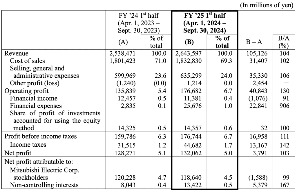
Mitsubishi Electric Corporation announced its consolidated financial results for the second quarter (first half), ended September 30, 2024, of the current fiscal year ending March 31, 2025 (fiscal 2025).
Original – Mitsubishi Electric
-

Ideal Power Inc. announced that the Company received orders from a global Tier 1 automotive supplier, a NYSE listed company. This global customer serves many automotive OEMs and is a leading supplier of sensors and electrical protection component solutions for automobile electrification and electric vehicles (EVs). They represent the latest addition to the Company’s customer list of Tier 1 suppliers targeting the EV market.
The Company is meeting regularly with this Tier 1 auto supplier and educating them on the benefits of B-TRAN™ in EV applications. As a result of these ongoing discussions, the customer placed orders for numerous discrete B-TRAN™ devices, a SymCool® power module, a solid-state circuit breaker evaluation board and a driver. This customer is interested in using B-TRAN™ for solid-state EV contactor applications.
“We are pleased to see another global Tier 1 automotive supplier securing B-TRAN™ products as part of their desire to bring lower cost, more efficient semiconductor solutions to their numerous automotive OEM customers. We are also working to advance other Tier 1 auto suppliers in our sales pipeline to orders and then to custom development agreements and/or design wins,” stated Dan Brdar, President and Chief Executive Officer of Ideal Power. “Overall, we are leveraging our success with Stellantis to attract and engage other auto OEMs as well as the Tier 1 auto suppliers that provide sub-systems to these global automakers.”
Contactors serve as cutoff switches for high voltage applications in EVs. They play a critical role in isolating the battery, inverter, and onboard charger to ensure safety when the vehicle is off or being serviced. In a collision, power must be shut off from downstream systems to prevent further complications or damage. Contactors are bidirectional and there are typically 4 to 6 high-power contactors in every EV. The high-power EV contactor market is forecasted to grow to over $3.7 billion in 2025 and the Company believes that, over time, solid-state contactors will potentially displace electromechanical contactors in half or more of this market.
Solid-state contactors provide several benefits over electromechanical contactors. They act much faster, thereby eliminating arcing and improving safety, and are more reliable as they do not include physical contacts subject to wear. In addition, they provide programmable settings for trip and current limits as well as built-in safety diagnostics. Solid-state contactors are also expected to cost less than electromechanical contactors in EV applications.
Original – Ideal Power
-

Navitas Semiconductor will showcase its latest innovations at the 2024 China Power Electronics and Energy Conversion Conference and the 27th Annual Academic Conference and Exhibition of the China Power Supply Society (CPEEC & CPSSC 2024), held in Xi’an from November 8th – 11th, 2024.
At ‘Planet Navitas’ (Booth 3-011), visitors can discover the AI Power Roadmap, which showcases the world’s first 8.5 kW OCP AI data center power supply implementing GaNSafe and Gen-3 Fast SiC MOSFETs, alongside the highest power density 4.5 kW AI data center power supply on the planet. Navitas also developed the ‘IntelliWeave’ patented digital control combined with high-power GaNSafe™ and Gen 3-Fast SiC MOSFETs, optimized for AI data center power supplies, enabling PFC peak efficiencies to 99.3% and reducing power losses by 30% compared to existing solutions.
Additionally, industry-leading solutions include a 6.6kW 2-in-1 EV on-board charger (OBC) utilizing a hybrid GaNSafe and GeneSiC design and fast-charging solutions for consumer electronics with the latest GaNSlim family.
The new GaNSlim family offers a highly integrated GaN solution with autonomous EMI control and loss-less sensing that enables the industry’s fastest, smallest, and most efficient solution in an optimized DPAK-4L package, ideal for mobile, consumer, and home appliance applications up to 500 W.
Enabled by over 20 years of SiC innovation leadership, GeneSiC technology leads on performance with the Gen-3 Fast SiC MOSFETs with ‘trench-assisted planar’ technology. This proprietary technology provides world-leading performance over temperature, delivering cool-running, fast-switching, and superior robustness to support up to 3x more powerful AI data centers and faster charging EVs.
As China’s premier power electronics event, CPSSC gathers industry leaders, researchers, and enterprises to explore breakthrough technologies shaping the future of power electronics. This year’s focus is on high-efficiency, high-power density solutions. “CPSSC is a key platform to showcase Navitas’ role in advancing power electronics,” said Charles Zha, VP & GM of Navitas China. “Our GaNSafe, GaNSlim, and Gen-3 Fast SiC technologies highlight our commitment to enabling higher efficiency, faster charging, and more powerful applications, aligning with CPSSC’s vision of powering the future.”
Navitas will also present technical papers and host industrial sessions, sharing insights into GaN and SiC technologies and their real-world applications.
Navitas’ CPSSC 2024 Program Highlights:
- November 10
- Paper Presentation:
Research on Parasitic False Turn-On Behaviour of SiC MOSFETs with 0V Turn-Off Gate Voltage
13:20-13:40 | Xiangyang Zhou, Bin Li, Xiucheng Huang, Jason Zhang - Industrial Session:
Bi-Directional GaN for Improving Efficiency in Micro-Inverters
14:30-15:00 | Simon Qin, Sr. Staff Application Engineer
- November 11
- Technical Presentation:
Achieving 99.4% Efficiency in GaN-based Interleaving CrM TTP PFC
08:30-09:00 | Wenhao Yu, Sr. Application Engineer - Technology Showcase:
GaNSlim IC: Redefining Efficiency in Cost-Effective Power Supplies
10:20-10:50 | Ye Hu, Technical Marketing Manager - Industry Insights:
Opportunities and Challenges of Single-Stage Converters for On-Board Chargers
13:00-13:30 | Justin Zhu, Sr. Technical Marketing Manager
Original – Navitas Semiconductor
-

Qorvo® announced financial results for the Company’s fiscal 2025 second quarter ended September 28, 2024.
On a GAAP basis, revenue for Qorvo’s fiscal 2025 second quarter was $1.047 billion, gross margin was 42.6%, operating income was $9.7 million, and loss per share was $0.18. On a non-GAAP basis, gross margin was 47.0%, operating income was $212.2 million, and diluted earnings per share was $1.88.
Bob Bruggeworth, president and chief executive officer of Qorvo, said, “In the September quarter, ACG successfully supported our largest customer’s seasonal smartphone ramp. In HPA, we expanded our D&A business while building a broad-based business in power management. In CSG, we maintained our leadership in Wi-Fi applications while investing to grow in diverse businesses including automotive solutions and SoCs for ultra-wideband and Matter. HPA and CSG are on pace to achieve mid-teen year-over-year growth in fiscal 2025.”
Grant Brown, chief financial officer of Qorvo, said, “In the September quarter, we exceeded the midpoint of guidance in revenue, gross margin and EPS. Looking forward, the flagship and premium tiers in the smartphone market are holding up well, however, content and ramp profiles vary by model, and we are experiencing unfavorable mix. We expect this to continue in the second half of fiscal 2025. In addition, in the mid and entry tiers of Android 5G smartphones, mix has shifted toward entry-tier 5G at the expense of mid-tier 5G. In our current view, we don’t expect this mix shift in Android 5G from mid-tier to entry-tier to reverse. As a result, we are taking appropriate actions, including factory consolidation and operating expense reductions as well as focusing on opportunities that align with our long-term profitability objectives. We currently expect full-year fiscal 2025 revenue and gross margin will be slightly down versus fiscal 2024.”
Qorvo’s current outlook for the December 2024 quarter is:
- Quarterly revenue of approximately $900 million, plus or minus $25 million
- Non-GAAP gross margin of approximately 45%
- Non-GAAP diluted earnings per share between $1.10 and $1.30
Original – Qorvo
-

Littelfuse, Inc. reported financial results for the third quarter ended September 28, 2024:
- Net sales of $567 million were down 7% versus the prior year period and organically
- GAAP diluted EPS was $2.32 and adjusted diluted EPS was $2.71
- Cash flow from operations was $80 million and free cash flow was $65 million
“In the third quarter, our global teams delivered strong execution and drove sales and earnings above our expectations,” said Dave Heinzmann, Littelfuse President and Chief Executive Officer. “While we see soft end market conditions extending into the fourth quarter, we remain focused on driving operational excellence while serving our global customer base and delivering meaningful new business wins. Our proven growth strategy, diversification efforts and strong technology capabilities position us to deliver top tier long-term stakeholder value.”
Based on current market conditions, for the fourth quarter the company expects Net sales in the range of $510 – $540 million, adjusted diluted EPS in the range of $1.90 – $2.10 and an adjusted effective tax rate of approximately 14%.
Original – Littelfuse
-

After announcing the world’s first 300-millimeter gallium nitride (GaN) power wafer and opening the world’s largest 200-millimeter silicon carbide (SiC) power fab in Kulim, Malaysia, Infineon Technologies AG has unveiled the next milestone in semiconductor manufacturing technology.
Infineon has reached a breakthrough in handling and processing the thinnest silicon power wafers ever manufactured, with a thickness of only 20 micrometers and a diameter of 300 millimeters, in a high-scale semiconductor fab. The ultra-thin silicon wafers are only a quarter as thick as a human hair and half as thick as current state-of-the-art wafers of 40-60 micrometers.
“The world’s thinnest silicon wafer is proof of our dedication to deliver outstanding customer value by pushing the technical boundaries of power semiconductor technology,” said Jochen Hanebeck, CEO at Infineon Technologies. “Infineon’s breakthrough in ultra-thin wafer technology marks a significant step forward in energy-efficient power solutions and helps us leverage the full potential of the global trends decarbonization and digitalization. With this technological masterpiece, we are solidifying our position as the industry’s innovation leader by mastering all three relevant semiconductor materials: Si, SiC and GaN.”
This innovation will significantly help increase energy efficiency, power density and reliability in power conversion solutions for applications in AI data centers as well as consumer, motor control and computing applications. Halving the thickness of a wafer reduces the wafer’s substrate resistance by 50 percent, reducing power loss by more than 15 percent in power systems, compared to solutions based on conventional silicon wafers.
For high-end AI server applications, where growing energy demand is driven by higher current levels, this is particularly important in power conversion: Here voltages have to be reduced from 230 V to a processor voltage below 1.8 V. The ultra-thin wafer technology boosts the vertical power delivery design, which is based on vertical Trench MOSFET technology and allows a very close connection to the AI chip processor, thus reducing power loss and enhancing overall efficiency.
“The new ultra-thin wafer technology drives our ambition to power different AI server configurations from grid to core in the most energy efficient way,” said Adam White, Division President Power & Sensor Systems at Infineon. “As energy demand for AI data centers is rising significantly, energy efficiency gains more and more importance. For Infineon, this is a fast-growing business opportunity. With mid-double-digit growth rates, we expect our AI business to reach one billion euros within the next two years.”
To overcome the technical hurdles in reducing wafer thickness to the order of 20 micrometers, Infineon engineers had to establish an innovative and unique wafer grinding approach, since the metal stack that holds the chip on the wafer is thicker than 20 micrometers. This significantly influences handling and processing the backside of the thin wafer.
Additionally, technical and production-related challenges like wafer bow and wafer separation have a major impact on the backend assembly processes ensuring the stability and first-class robustness of the wafers. The 20-micrometer thin wafer process builds on Infineon’s existing manufacturing expertise and ensures that the new technology can be seamlessly integrated into existing high-volume Si production lines without incurring additional manufacturing complexity, thus guaranteeing the highest possible yield and supply security.
The technology has been qualified and applied in Infineon’s Integrated Smart Power Stages (DC-DC converter) which have already been delivered to first customers. It underlines the company’s innovation leadership in semiconductor manufacturing as the holder of a strong patent portfolio related to the 20-micrometer wafer technology.
With the current ramp up of the ultra-thin wafer technology Infineon expects a replacement of the existing conventional wafer technology for low voltage power converters within the next three to four years. This breakthrough is bolstering Infineon’s unique position in the market with the broadest product and technology portfolio including silicon, silicon carbide and gallium nitride-based devices which are key enablers of decarbonization and digitalization.
Infineon will present the first ultra-thin silicon wafer publicly at electronica 2024 from 12 to 15 November in Munich (Hall C3, Stand 502).
Original – Infineon Technologies
-

onsemi announced its wafer fab in East Fishkill (EFK), New York, has been accredited by the Defense Microelectronics Activity (DMEA) of the U.S. Department of Defense (DoD) as a Category 1A Trusted Supplier. The accreditation enables onsemi to manufacture secure advanced semiconductors for a variety of critical aerospace and defense applications at the site. onsemi’s East Fishkill fab is the only 300 mm power discrete and image sensor fab in the U.S. and the company’s second accredited fab in addition to its Gresham, Oregon site.
“Power and sensing technologies are vital in modern defense systems, providing the reliable energy and data required for robust, intelligent and efficient operations,” said Sudhir Gopalswamy, group president Intelligent Sensing and Analog and Mixed-Signal Groups of onsemi. “With this accreditation, onsemi is now positioned to offer our industry-leading power and sensing technologies through our secure and trusted manufacturing facilities that will enable the DoD to have the reliable and cutting-edge solutions they need.”
Achieving the trusted foundry accreditation is a rigorous process that ensures a supplier meets comprehensive security and operational criteria, including the protection of mission-critical functions for trusted systems and networks. This thorough approach safeguards the integrity and confidentiality of onsemi’s industry-leading intelligent power and sensing technologies. As a trusted supplier, onsemi is able to provide custom-designed, custom-manufactured or tailored power and sensing solutions for specific DoD applications.
Original – onsemi
-

At the upcoming electronica trade show in Munich, Infineon Technologies AG will illustrate how its innovative solutions are driving the global trends of decarbonization and digitalization. The company will show how its semiconductors are paving the way to a net-zero economy and to unlocking the full potential of artificial intelligence (AI). From 12 to 15 November at booth 502 in hall C3, Infineon will present highlights from its extensive portfolio and offer the opportunity to talk to its experts.
“Decarbonization and digitalization are the key drivers on the way to a climate-neutral future,” said Andreas Urschitz, Member of the Board and Chief Marketing Officer at Infineon. “Semiconductors contribute in many ways to the green and digital transformation and are at the heart of every connected application. At electronica, we’ll be showcasing how our leading technologies and innovative solutions are helping master the central challenges of our time.”
World’s first 300 mm gallium nitride wafers
Infineon will present its technological breakthrough, the world’s first 300 mm power gallium nitride (GaN) wafer technology, to the general public for the first time. This technological milestone will significantly advance the market for GaN-based power semiconductors. Leveraging 300 mm GaN will strengthen existing solutions and application fields and create new ones, with an increasingly cost-effective value proposition and the ability to address the full range of customer systems.
Shaping the future of mobility
Infineon is focused on the development of innovative solutions that drive the transition to clean, safe and intelligent mobility. Products and solutions on display at electronica include the new AURIX™ TC4x microcontrollers, which support the implementation of future-proof E/E architectures and software-defined vehicles, as well as the main inverter CoolSiC™ Kit, battery management system solutions, on-board chargers with GaN, steer-by-wire system solutions and H 2 sensors for fuel cell applications.
Greener and smarter buildings and homes
Semiconductors play a crucial role in the development of smarter and more sustainable living spaces. Infineon’s advanced technologies based on silicon carbide (SiC) and GaN enable maximum energy efficiency and reliability for energy generation and consumption.
With advanced sensors, power semiconductors, security solutions such as OPTIGA™ Trust and microcontrollers such as PSOC™ Control, Infineon enables the efficient use of green energy while bringing smart automation to modern homes and commercial buildings. The company’s booth will showcase comprehensive system solutions including various solar inverter topologies (micro-inverters and string inverters), as well as demos for optimizing power and boosting heat pump output.
Enabling AI – Efficient, reliable and on the edge
Semiconductors also play a crucial role in unlocking the full potential of AI. Infineon’s solutions make it possible for customers to deploy new AI applications quickly, efficiently and at scale. The company’s broad range of products, software, tools and services enables energy-efficient data centers, smarter devices and optimized AI edge applications. Demos will include high-performance, low-power AI-enabled microcontrollers from the PSOC family, advanced sensors from the XENSIV™ portfolio as well as vertical power module architectures, advanced liquid cooling modules and power supply units for AI data centers.
Visitors who are unable to attend the live show can register here for Infineon’s digital event platform, which will be available 24/7.
More information about Infineon’s show highlights is available at www.infineon.com/electronica.
Original – Infineon Technologies
