• U.S. Department of Commerce’s Bureau of Industry and Security Strengthens Semiconductor Export Controls

    U.S. Department of Commerce’s Bureau of Industry and Security Strengthens Semiconductor Export Controls

    7 Min Read

    The U.S. Department of Commerce’s Bureau of Industry and Security (BIS) announced a package of rules designed to further impair the People’s Republic of China’s (PRC) capability to produce advanced-node semiconductors that can be used in the next generation of advanced weapon systems and in artificial intelligence (AI) and advanced computing, which have significant military applications. This action is a proactive measure enhancing the Department of Commerce’s work to impede the PRC’s ability to procure and produce the technologies necessary for its military modernization.

    The rules include new controls on 24 types of semiconductor manufacturing equipment and 3 types of software tools for developing or producing semiconductors; new controls on high-bandwidth memory (HBM); new red flag guidance to address compliance and diversion concerns; 140 Entity List additions and 14 modifications spanning PRC tool manufacturers, semiconductor fabs, and investment companies involved in advancing the PRC government’s military modernization; and several critical regulatory changes to enhance the effectiveness of our previous controls.

    “This action is the culmination of the Biden-Harris Administration’s targeted approach, in concert with our allies and partners, to impair the PRC’s ability to indigenize the production of advanced technologies that pose a risk to our national security,” said U.S. Secretary of Commerce Gina Raimondo. “Further strengthening our export controls underscores the central role of the Department of Commerce in executing the United States’ broader national security strategy. No Administration has been tougher in strategically addressing China’s military modernization through export controls than the Biden-Harris Administration.”

    “The United States has taken significant steps to protect our technology from being used by our adversaries in ways that threaten our national security. As technology evolves, and our adversaries seek new ways to evade restrictions, we will continue to work with our allies and partners to proactively and aggressively safeguard our world-leading technologies and know-how so they aren’t used to undermine our national security,” said National Security Advisor Jake Sullivan.

    “This action builds on BIS’s laser-focused work, undertaken over the past few years, to impose strategic controls that have hindered the PRC’s ability to produce advanced semiconductors and AI capabilities directly impacting U.S. national security. We are constantly talking to our allies and partners as well as reassessing and updating our controls. Today’s announcement represents the next step in that ongoing work,” said Under Secretary of Commerce for Industry and Security Alan Estevez. “This package is proactive and innovative in how we are responding to increasingly sophisticated actors and complex supply chains. We must ensure that we stay ahead of the PRC by protecting our advanced technology.”

    “The PRC’s Military-Civil Fusion strategy presents a significant risk that advanced node semiconductors will be used in military applications that threaten the security of the United States, as well as the security of our allies and partners,” said Assistant Secretary of Commerce for Export Administration Thea D. Rozman Kendler. “These rules build on previous actions taken in service of our longstanding goal: protecting our collective security by constraining the PRC’s ability to indigenize the most advanced technologies, without unduly interfering with the continuing trade of technology.”

    “The purpose of these Entity List actions is to stop PRC companies from leveraging U.S. technology to indigenously produce advanced semiconductors,” said Matthew S. Axelrod, Assistant Secretary for Export Enforcement. “By adding key semiconductor fabrication facilities, equipment manufacturers, and investment companies to the Entity List, we are directly impeding the PRC’s military modernization, WMD programs, and ability to repress human rights.”

    Taking Novel Approaches to Impair and Impede the PRC’s Military Modernization

    Throughout the Biden-Harris Administration, in coordination with U.S. allies and partners, BIS has taken novel approaches to address an ever-changing geopolitical and technological landscape and respond to increasingly sophisticated threat actors.

    All of the policy changes announced today are designed to limit the PRC’s ability to indigenize the production of advanced technologies – such as advanced-node integrated circuits and the equipment used to produce them – that pose a substantial risk to U.S. national security. The semiconductor manufacturing equipment controlled by today’s rules is needed to produce advanced-node integrated circuits, which are necessary for advanced weapon systems and advanced AI used in military applications.

    Advancements in large-scale AI models have shown striking performance improvements across many human abilities and may be used in advanced military and intelligence applications. These models have the ability to rapidly review and synthesize large amounts of information into actionable points. Advanced AI models could be used for rapid response scenarios on the battlefield; lowering the barrier to develop cyberweapons or chemical, biological, radiological, or nuclear weapons; and utilizing facial and voice recognition to repress and surveil minorities and political dissidents.

    This announcement underscores the United States’ “small yard, high fence” strategy and will restrict the PRC’s ability to produce technologies key to its military modernization or repression of human rights.

    These actions serve two primary objectives:

    • Slowing the PRC’s development of advanced AI that has the potential to change the future of warfare; and
    • Impairing the PRC’s development of an indigenous semiconductor ecosystem – an ecosystem built at the expense of U.S. and allied national security.

    In line with these objectives, BIS is implementing several regulatory measures, including but not limited to:

    • New controls on semiconductor manufacturing equipment needed to produce advanced-node integrated circuits, including certain etch, deposition, lithography, ion implantation, annealing, metrology and inspection, and cleaning tools.
    • New controls on software tools for developing or producing advanced-node integrated circuits, including certain software that increases the productivity of advanced machines or allows less-advanced machines to produce advanced chips.
    • New controls on high-bandwidth memory (HBM). HBM is critical to both AI training and inference at scale and is a key component of advanced computing integrated circuits (ICs). The new controls apply to U.S.-origin HBM as well as foreign-produced HBM subject to the EAR under the advanced computing Foreign Direct Product (FDP) rule. Certain HBM will be eligible for authorization under new License Exception HBM.
    • Addition of 140 entities to the Entity List, in addition to 14 modifications, including semiconductor fabs, tool companies, and investment companies that are acting at the behest of Beijing to further the PRC’s advanced chip goals which pose a risk to U.S. and allied national security.
    • Establishment of two new Foreign Direct Product (FDP) rules and corresponding de minimis provisions:
      • Semiconductor Manufacturing Equipment (SME) FDP: Extends jurisdiction over specified foreign-produced SME and related items if there is “knowledge” that the foreign-produced commodity is destined to Macau or a destination in Country Group D:5, including the PRC
      • Footnote 5 (FN5) FDP: Extends jurisdiction over specified foreign-produced SME and related items if there is “knowledge” of certain involvement by an entity on or added to the Entity List with a FN5 designation. Such entities are being designated on the Entity List for specific national security or foreign policy concerns described in the Entity List companion rule, such as these entities’ involvement in supporting the PRC’s military modernization through the PRC’s attempts to produce advanced-node semiconductors, including for military end-uses.  
      • De minimis: Extends jurisdiction over specified foreign-produced SME and related items described in the above FDP rules that contain any amount of U.S.-origin integrated circuits.
    • New software and technology controls, including restrictions on Electronic Computer Aided Design (ECAD) and Technology Computer Aided Design (TCAD) software and technology when there is “knowledge” that such items will be used for the design of advanced-node integrated circuits to be produced in Macau or a destination in Country Group D:5.
    • Clarification to the EAR regarding existing controls on software keys. Export controls now apply to the export, reexport, or transfer (in-country) of software keys that allow access to the use of specific hardware or software or renewal of existing software and hardware use licenses.

    In October 2022, BIS published an interim final rule (IFR) to restrict the PRC’s ability to both purchase and manufacture certain high-end semiconductors critical for military applications. As part of BIS’s commitment to continually evaluating the effectiveness of export controls, it released updated rules in October 2023 and April 2024. Today’s rules build on those efforts.

    Original – Bureau of Industry and Security

    Comments Off on U.S. Department of Commerce’s Bureau of Industry and Security Strengthens Semiconductor Export Controls
  • Power Master Semiconductor Expands eSiC MOSFET Family with AEC-Q101 Qualified TSPAK

    Power Master Semiconductor Expands eSiC MOSFET Family with AEC-Q101 Qualified TSPAK

    3 Min Read

    Power Master Semiconductor has announced the expansion of its e SiC MOSFET family with introduction of new AEC-Q101 qualified, high-performance top-side cooling packages. These include the TSPAK DBC version and LF version, specially designed for automotive and industrial applications.

    The TSPAK offers superior thermal performance, high efficiency, power density and reliability, making it ideal for a variety of automotive applications such as on-board chargers (OBCs), DC-DC converters, and e-compressors. This innovative packaging leverages Power Master Semiconductor’s latest generation of 1200V eSiC MOSFET (Gen2), employing cutting-edge technology to decouple a trade-off between specific on-resistance (Rsp) and short-circuit withstand time (SCWT). Compared to the previous generation, the new 1200V eSiC MOSFETs deliver 20% reduction in RDS(ON) and a 15% improvement in SCWT, as well as a 45% reduction in switching losses.

    Key Features and Benefits of TSPAK

    TSPAK LF version

    • Top-side cooling package with an exposed drain at the surface, allowing direct heat dissipation to the heatsink.
    • Offers superior thermal performance and supports high current capabilities.
    • High temperature capability : Tj (max)= 175°C
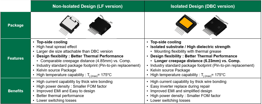
    TSPAK DBC version

    • Integrates an isolated DBC ceramic pad on the surface, providing premium thermal performance and enhanced design flexibility.
    • Features 3.6kV isolation voltage, extended creepage distance (5.23mm), and flexible mounting by directly connected to an external heatsink with thermal grease.
    • High temperature capability : Tj (max)= 175°C

    With an industry-standard footprint of 14mm x 18.58mm, the TSPAK packages provide superior thermal performance and Kelvin source configuration to minimizes gate noise and reduces turn-on losses by 60%, enabling higher-frequency operation and improved power density.

    The PCR120N40M2A (LF version) and PCRZ120N40M2A (DBC version) are automotive-grade 1200V/40mΩ eSiC MOSFETs in TSPAK packages, leveraging Power Master Semiconductor’s 2nd-generation eSiC MOSFET technology to deliver optimized performance for the automotive systems.

    • E-compressors, vital for efficient thermal management, extended battery life, enhanced charging efficiency, and improved driving range.
    • Totem-Pole PFC and CLLC/DAB (Dual Active Bridge) topologies, essential for bidirectional power conversion in 800V battery systems used in electric vehicles.

    “Cooling is one of the greatest challenges in high power design and successfully addressing it is the key enabler to reducing size and weight, which is critical in modern automotive design” said Namjin Kim, Senior Director of Sales & Marketing. “Our new top-side cooling package offer better system efficiency and minimize heat thermal path on the PCB, the system design will be simplified and compacted. We are confident that this innovative solution will be the optimal choice for high-performance automotive applications.”

    “Efficient cooling is a critical challenge for reducing size and weight of high-power automotive systems,” said Namjin Kim, Senior Director of Sales & Marketing. “Our new top-side cooling package enhances system efficiency and minimizes the thermal path on the PCB, enabling simpler, more compact system designs. We believe this innovative solution will drive the high performance automotive applications.”

    Original – Power Master Semiconductor

    Comments Off on Power Master Semiconductor Expands eSiC MOSFET Family with AEC-Q101 Qualified TSPAK
  • Fuji Electric and DENSO Jointly Invest into Production of SiC Power Semiconductors

    Fuji Electric and DENSO Jointly Invest into Production of SiC Power Semiconductors

    2 Min Read

    DENSO Corporation and Fuji Electric Co., Ltd. announced that a semiconductor supply plan submitted jointly by the companies has been approved by the Ministry of Economy, Trade and Industry. Under this plan, the companies will take part in joint investment and production of silicon carbide (SiC) power semiconductors to develop and strengthen frameworks for the supply of said semiconductors.

    Power semiconductors are vital to the efficient supply of electric power. Demand for power semiconductors has been rising rapidly given that they are used in electrified vehicles, which are being adopted at an accelerated pace amid the push for the decarbonization of society. In comparison to prior silicon semiconductors, SiC power semiconductors are able to deliver superior performance under high temperature, high-frequency, and high-voltage conditions.

    These devices are therefore anticipated to make large contributions to reductions in power loses as well as to more compact and lighter-weight designs for battery electric vehicle systems and other power electronics. Accordingly, growth in demand is projected for SiC power semiconductors.

    In response to electrification trends, DENSO has advanced SiC technology development projects targeting increased quality and efficiency in relation to everything from wafers and element devices to modules and inverters. Meanwhile, Fuji Electric has constructed extensive frameworks encompassing all tasks spanning from the development of SiC power semiconductor elements that enable increased efficiency and more compact designs for power electronics equipment to mass production of the related modules.

    Based on the approved plan, these companies will combine their respective automotive product development and production technology capabilities in a joint effort to expand their capacity for the efficient and stable supply of SiC power semiconductors throughout Japan.

    Through this partnership, the companies will contribute to the development of semiconductor supply frameworks within Japan and to the improvement of the international competitiveness of Japan’s domestic semiconductor and automotive industries. In addition, this partnership is anticipated to help advance the decarbonization of society.

    Original – Fuji Electric

    Comments Off on Fuji Electric and DENSO Jointly Invest into Production of SiC Power Semiconductors
  • Infineon Technologies Received German Sustainability Award

    Infineon Technologies Received German Sustainability Award

    3 Min Read

    Infineon Technologies AG has won the German Sustainability Award in the “Electrical Engineering and Electronics” category. “The jury is of the opinion that Infineon has assumed a leading role in the field of sustainability and serves the sector as a ‘beacon’ for successful transformation,” the judges said in their statement. The German Sustainability Award recognizes companies which make effective and exemplary contributions to transformation and which function as role models within their industry.

     “We are particularly honored and delighted to win the German Sustainability Award,” said Elke Reichart, Member of the Management Board and Chief Digital and Sustainability Officer at Infineon, who accepted the award in Duesseldorf. “We at Infineon work hard to drive decarbonization and digitalization and to create a more sustainable future. This award is recognition, as well as an incentive to be a role model in sustainability and to continue rigorously implementing our ambitious sustainability strategy – together with our employees, customers and partners.”

    Infineon is pursuing a comprehensive and ambitious decarbonization strategy. The company is making good progress towards the goal it defined in 2020: achieving climate neutrality by 2030. Since then, emissions have been reduced by more than two thirds while revenue has almost doubled. Moreover, Infineon is intensifying its collaboration along the entire supply chain. As a pioneer in its industry, Infineon this year began reporting emissions at the individual product level, referred to as the Product Carbon Footprint. The data is already available for half of all Infineon products today.

    Infineon’s semiconductors are decisive in making the generation, transmission, storage and use of energy more efficient. A recent example of sustainable product innovation by Infineon is a new type of energy-saving silicon carbide (SiC) module, whose developers were nominated for the 2024 Deutscher Zukunftspreis. The solution increases the energy efficiency of existing high-performance electrical applications such as solar and wind power plants and train drives. Among other things, the module also facilitates the efficient electrification of large drives such as those found in agricultural and construction machinery, ships and aircraft. In concrete terms, a single electric locomotive equipped with the new drive system saves around 300 megawatt hours per year, which corresponds to the annual energy requirements of 100 single-family homes.

    The German Sustainability Award is Europe’s largest award for ecological and social commitment. The jury of the German Sustainability Award (DNP) selected winners in 100 different sectors from among around 2000 competing companies. The German Sustainability Award works together with the German Chamber of Industry and Commerce (DIHK), WWF Germany, PwC Germany, Leuphana University Lüneburg (CSM Lüneburg) and numerous other industry associations to design and implement the competition.

    Current reports on sustainability at Infineon can be found here.

    Original – Infineon Technologies

    Comments Off on Infineon Technologies Received German Sustainability Award