-

Infineon Technologies AG has completed the sale of its two backend manufacturing sites, one in Cavite, Philippines and one in Cheonan, South Korea, to two fully owned subsidiaries of ASE, a leading provider of independent semiconductor manufacturing services in assembly and test.
ASE will assume operations with current employees, and further develop both sites to support multiple customers. As such, ASE and Infineon have also concluded long-term supply agreements under which Infineon will continue to receive previously established services as well as services for new products to support its customers and fulfill existing commitments.
Original – Infineon Technologies
-

Magnachip Semiconductor Corporation announced financial results for the second quarter 2024.
YJ Kim, Magnachip’s CEO, commented, “Our Q2 revenue was above the mid-point of guidance and gross margin was better than expected. Revenue in our Standard Products Business, which is comprised of our MSS and PAS businesses, increased sequentially by double digits in Q2. We benefited from a recovery in our Power business, increased demand for OLED drivers for China smartphones and European autos, and an upturn in Power IC demand for OLED IT panels and LED TVs.”
YJ Kim added, “Looking ahead, we currently expect Standard Product Business revenue will increase sequentially once again in Q3, driven by leaner distribution channels in Power, as well as seasonality, and an increase in OLED and Power IC businesses.”
Financial Highlights
- Q2 consolidated revenue was $53.2 million, above the mid-point of guidance range of $49-54 million.
- Q2 standard product business revenue was up 11.6% sequentially.
- Q2 consolidated gross profit margin was 21.8%, above the upper end of guidance range of 17-19%.
- Q2 standard product business gross profit margin was 23.1%, up nearly two percentage points sequentially.
- Ended Q2 with cash of $132.5 million; and also have an additional short-term financial investment of $30 million.
- Repurchased approximately 0.5 million shares for aggregate purchase price of $2.3 million during the quarter.
Operational Highlights
- Held formal opening ceremony in China for newly formed subsidiary, Magnachip Technology Company, Ltd. (MTC).
- Secured a purchase commitment for OLED driver targeted for a premium smartphone OEM; mass production and revenue currently expected to begin by year-end.
- Delivered samples of our next-generation OLED driver to a panel supplier for a leading Chinese smartphone OEM’s winter 2024 model, now in the final design validation phase.
- Taped out a new OLED driver designed with next-generation IP including sub-pixel rendering (SPR), refined color enhancement, color filter, brightness uniformity control and more than 20% reduction in power consumption than previous generation.
- Sampled our first OLED smartwatch DDIC in Q2 following a Q1 tape-out, demonstrating our expansion into new, adjacent markets.
- Power IC revenue increased sequentially, driven primarily by demand for LCD TVs and OLED IT monitors.
- Sequential revenue growth in PAS segment was driven by industrial, communication and consumer applications. Automotive rebounded with new design wins in Japan and China.
- Launched new 75A/1200V IGBT for a design opportunity in solar applications; expected to begin mass production in the second half of the year.
Original – Magnachip Semiconductor
- Q2 consolidated revenue was $53.2 million, above the mid-point of guidance range of $49-54 million.
-

Amkor Technology, Inc. announced financial results for the second quarter ended June 30, 2024.
Second Quarter 2024 Highlights
- Net sales $1.46 billion
- Gross profit $212 million, operating income $82 million
- Net income $67 million, earnings per diluted share $0.27
- EBITDA $247 million
“Amkor delivered second quarter results in line with expectations. Revenue of $1.46 billion was up 7% sequentially, driven by Advanced packaging supporting premium tier smartphones and AI solutions utilizing 2.5D technology,” said Giel Rutten, Amkor’s president and chief executive officer. “Strength in the Communications and Computing end markets was partially offset by soft demand and ongoing inventory corrections in the Automotive & Industrial and Consumer end markets.”
At June 30, 2024, total cash and short-term investments was $1.5 billion, and total debt was $1.1 billion.
The company paid a quarterly dividend of $0.07875 per share on June 24, 2024. The declaration and payment of future dividends, as well as any record and payment dates, are subject to the approval of the Board of Directors.
Business Outlook
The following information presents Amkor’s guidance for the third quarter 2024 (unless otherwise noted):
- Net sales of $1.785 billion to $1.885 billion
- Gross margin of 14.0% to 16.0%
- Net income of $105 million to $140 million, or $0.42 to $0.56 per diluted share
- Full year 2024 capital expenditures of approximately $750 million
Original – Amkor Technology
-

DENSO announced global financial results for its first quarter, ending June 30, 2024, for its 2025 fiscal year, ending March 31, 2025:
- Consolidated revenue totaled 1,753.8 billion yen (US$10.9 billion), a 2.4 percent increase from the previous year.
- Consolidated operating profit totaled 120.6 billion yen (US$0.7billion), a 27.7 percent increase from the previous year.
- Consolidated profit attributable to owners of the parent company totaled 94.5billion yen (US$0.6billion), a 10.5 percent increase from the previous year.
“Revenue in the first quarter increased compared to the previous year, due in part to slowing depreciation of the yen, though suspensions of operations by Japanese customers and lower vehicle production volumes due to poor vehicle sales in Asia did affect overall performance. Operating profit in the first quarter increased compared to the previous year due to foreign exchange gains and improvement efforts though lower production volumes.” said Yasushi Matsui, CFO, Vice President and member of the Board of Directors of DENSO CORPORATION.
“In this fiscal year, we forecast 7,330.0 billion yen (US$45.5 billion) in revenue and 692.0 billion yen (US$4.3 billion) in operating profit. In the first quarter, due to the idling of Japanese customers and lower vehicle production volumes in Asia, both sales revenue and operating profit decreased compared to the announced forecast at the beginning of the year. And from the second quarter onward, the impact of suspended operations by customers in Japan is expected to be reduced, but poor vehicle sales, especially in Asia, are expected to continue. On the other hand, the yen is also expected to continue to depreciate. As we navigate these uncertainties, we commit to execute our plan from the second quarter onward announced at the beginning of the year. Based on the above, our forecast of revenue and operating profit reflects only the downside of the first quarter and revise full-year financial forecast downward.”
- In Japan, revenue increased to 984.6illion yen (US$6.1 billion), up 0.4% from the previous year, and operating profit was 45.1 billion yen (US$280.0 million), up 81.6% from the previous year.
- In North America, revenue increased to 500.1 billion yen (US$3.1 billion), up 17.7% from the previous year, and operating profit was 23.3 billion yen (US$144.6 million) up 270.2% from the previous year.
- In Europe, revenue increased to 199.8 billion yen (US$1.2 billion), up 0.7% from the previous year, and operating profit was 5.0 billion yen (US$31.0 million), down 33.0% from the previous year.
- In Asia, revenue increased to 461.4 billion yen (US$2.9 billion), down 0.6% from the previous year and operating profit was 35.8 billion yen (US$222.0 million), down 11.7% from the previous year.
- In other areas, revenue increased to 29.0 billion yen (US$0.2 billion), up 1.8% from the previous year, and operating profit was 5.9 billion yen (US$36.9 million), up 19.5% from the previous year.
Original – DENSO
-

Littelfuse, Inc. reported financial results for the second quarter ended June 29, 2024:
- Net sales of $558 million were down 9% versus the prior year period, and down 8% organically
- GAAP diluted EPS was $1.82 and adjusted diluted EPS was $1.97
- Cash flow from operations was $69 million and free cash flow was $50 million
- The company’s Board of Directors approved an 8% increase in the quarterly cash dividend from $0.65 to $0.70; this equates to an annualized dividend of $2.80 per share
- On June 26, the company released its 2023 Sustainability Report on littelfuse.com/about-us/sustainability
“We are pleased to have exceeded the high end of our second quarter sales and adjusted EPS guidance ranges, driven by solid execution from our global teams and supported by our resilient business model and diverse technology positioning.” said Dave Heinzmann, Littelfuse President and Chief Executive Officer. “Looking ahead, we remain confident in an expected return to growth during 2024, likely in the fourth quarter. We see some pockets of normalized channel inventory and improving end demand but also ongoing signs of cautiousness from customers. We remain well positioned to execute our proven long-term growth strategy and deliver top tier stakeholder value.”
Original – Littelfuse
-

Mitsubishi Electric Corporation announced its consolidated financial results for the first quarter, ended June 30, 2024, of the current fiscal year ending March 31, 2025 (fiscal 2025).
- Q1 FY25: Revenue ¥1,286.4 bn (+¥66.1 bn YoY), Operating Profit ¥58.6 bn (-¥2.3 bn YoY)
- Revenue achieved a new record high due primarily to an increase in the infrastructure segment and the impact of the weaker yen.
- Operating profit remained at the same level YoY due to the impact of a decrease in volume in the factory automation systems business and the impact of rising material and other procurement costs.
- FY25 forecast: Revenue ¥5,390.0 bn (+¥90.0 bn compared to the previous forecast), Operating Profit ¥400.0 bn (unchanged from the previous announcement)
- The revenue forecast has been revised upward partly due to a reconsideration of foreign exchange rates, while incorporating the impact of the delay in market recovery for factory automation systems.
- The company will steadily implement initiatives to achieve earnings targets, including improvements in product prices to reflect the impact of rising procurement costs.
Semiconductor & Device Segment
Revenue (YoY), Billions of yen Operating profit (YoY),
Billions of yenOperating profit margin (YoY), Billions of yen 74.5(+6.3) 11.5(+4.8) 15.5%(+5.7pt) - The market saw robust demand for power modules used in railway & power transmission applications.
- Orders decreased YoY due primarily to a decrease in power modules. Revenue increased YoY due mainly to the impact of the weaker yen as well as an increase in power modules used in automotive applications and other factors.
- Operating profit increased YoY due mainly to increased revenue.
Original – Mitsubishi Electric
-

JEDEC Solid State Technology Association announced that its JC-15 Committee for Thermal Characterization Techniques for Semiconductor Packages welcomes interested companies to join JEDEC and participate in committee meetings and activities.
Near-term plans for the committee include the evolution of standards that cover the provision of electronic thermal models in neutral file formats (e.g. JEP181, JEP30 T101), as well as the review and improvement of several key standards previously developed by the committee. For more information about JC-15 activities and JEDEC membership visit the JEDEC website.
Activities within JC-15’s scope include the standardization of thermal characterization techniques, both testing and modeling, for electronic packages, components, and materials for semiconductor devices.
“The activities of JC-15 reflect JEDEC’s commitment to evolving alongside the dynamic microelectronics industry,” said Robin Bornoff, Acting Chair of the JC-15 Committee. He added, “The wide range of subjects covered by JC-15 standards provides our members with diverse opportunities to contribute their knowledge and expertise to further enhance the efficacy of the electronics thermal supply chain.”
Original – JEDEC
-

Qorvo® announced financial results for the Company’s fiscal 2025 first quarter ended June 29, 2024.
Strategic Highlights
- Grew quarterly revenue 36% year-over-year and exceeded mid-point of revenue guidance by $37 million
- Transitioned Beijing and Dezhou operations to Luxshare and integrated Anokiwave into Qorvo
On a GAAP basis, revenue for Qorvo’s fiscal 2025 first quarter was $887 million, gross margin was 37.5%, operating income was $4.6 million, and diluted earnings per share was $0.00. On a non-GAAP basis, gross margin was 40.9%, operating income was $98.1 million, and diluted earnings per share was $0.87.
Bob Bruggeworth, president and chief executive officer of Qorvo, said, “During the June quarter, we fully integrated Anokiwave into Qorvo, adding silicon beam-forming ICs and IF-RF conversion products. We are investing in technology leadership to broaden our market exposure and drive growth, and we are executing on cost and productivity initiatives to structurally enhance our gross margin.”
Financial Commentary and Outlook
Grant Brown, chief financial officer of Qorvo, said, “Qorvo exceeded the mid-point of June quarterly guidance for revenue, gross margin and EPS. For the September quarter, we expect sequential increases in revenue, gross margin and EPS. We are leveraging internal factories which are critical differentiators for each of our operating segments, while outsourcing to our robust foundry and OSAT partner network where we benefit from their scale and R&D investments.”
Qorvo’s current outlook for the September 2024 quarter is:
- Quarterly revenue of approximately $1.025 billion, plus or minus $25 million
- Non-GAAP gross margin between 46% and 47%
- Non-GAAP diluted earnings per share between $1.75 and $1.95
Original – Qorvo®
-
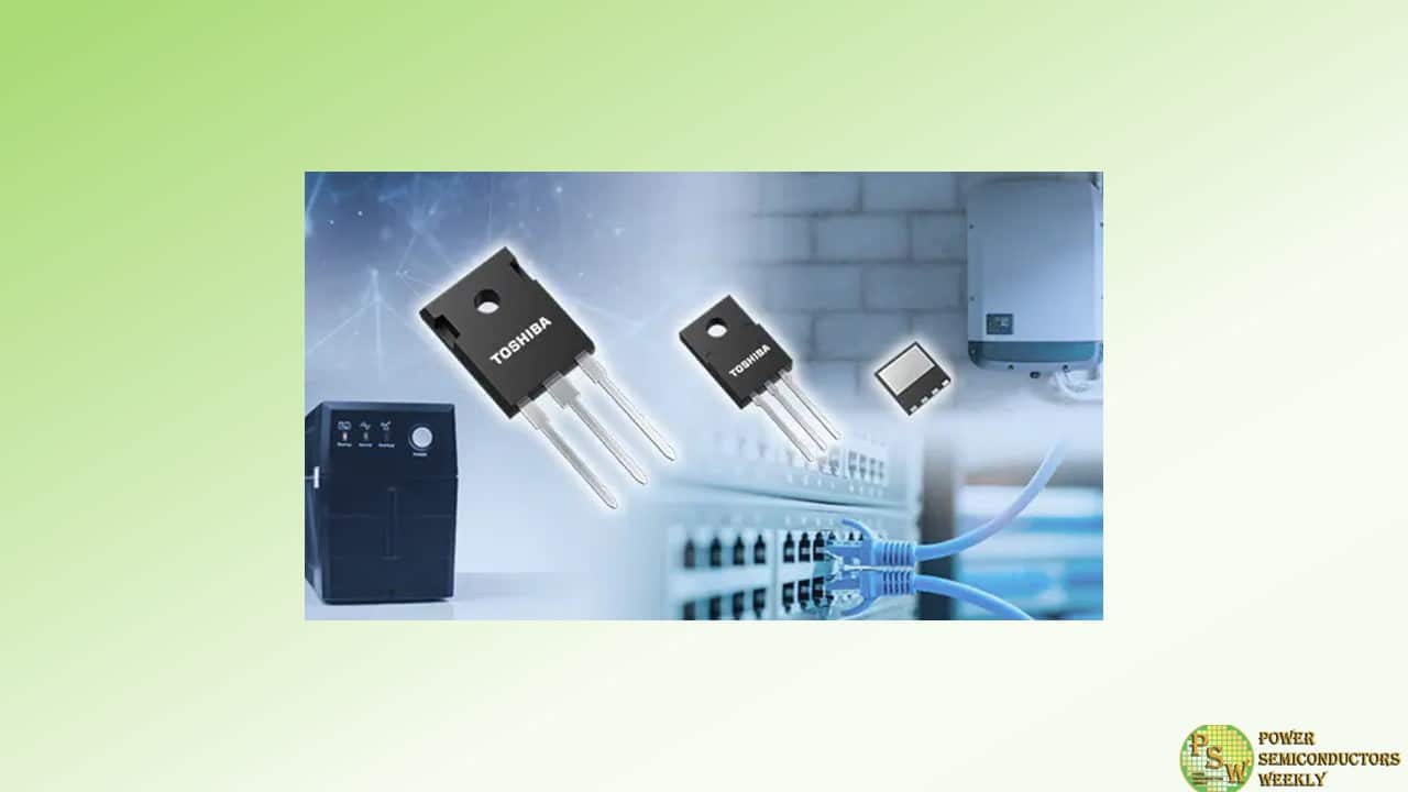
Toshiba Electronic Devices & Storage Corporation has expanded its lineup of 600V N-channel power MOSFETs “DTMOSVI series” fabricated with Toshiba’s latest-generation process, with a super junction structure. These new products are suitable for high efficiency switching power supplies used for data centers and power conditioners of photovoltaic generators. Nine products of “TK40N60Z1, TK080N60Z1, TK080A60Z1, TK085V60Z1, TK125N60Z1, TK125A60Z1, TK130V60Z1, TK155A60Z1 and TK165V60Z1” have been added to the lineup in terms of packages and drain-source On-resistance.
By optimizing the gate design and process, 600V DTMOSVI series products have reduced the value of drain-source On-resistance per unit area by approximately 13%, and drain-source On-resistance × gate-drain charge ―the figure of merit for MOSFET performance― by approximately 52% compared to Toshiba’s current generation DTMOSIV-H series products with the same drain-source voltage rating. This means new products have a better trade-off between conduction loss and switching loss than current products. New products of DTMOSVI series will contribute improving efficiency of power supplies.
Toshiba offers tools that support circuit design for switching power supplies. Alongside the G0 SPICE model, which verifies circuit function in a short time, highly accurate G2 SPICE models that accurately reproduce transient characteristics are now available.
Toshiba will continue to expand its DTMOSVI series lineup, and support energy conservation by reducing power loss in switching power supplies.
Original – Toshiba
-
According to a survey by Global Market Insights, Super Junction MOSFETs captured over 30% market share in the energy and power sector in 2023. Their applications span multiple domains, including electric vehicle charging stations, server and data center power supplies, LED drivers, solar inverters and home appliance controls.
The global Super Junction MOSFET market is projected to achieve a compound annual growth rate (CAGR) exceeding 11.5% by 2032. Super Junction MOSFETs offers robust assurance to customers seeking exceptional performance and stability backed by WeEn’s well-established reliability standards, comprehensive supply chain systems and continuously evolving technological roadmaps.
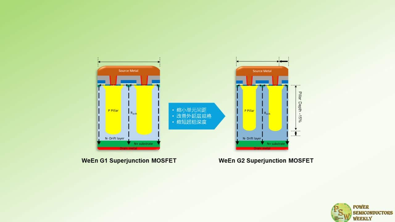
WeEn currently offers two series of Super Junction MOSFETs: G1 and G2. G2 Super Junction MOSFETs feature advanced design improvements, such as reduced cell pitch, low-resistance epitaxial layers, and shorter P-column depths. These innovations significantly reduce the device’s on-state resistance.
Simultaneously, WeEn precisely controlled the charge balance of the super junction structure, ensuring excellent avalanche ruggedness and low capacitive losses. This results in a balanced, outstanding performance in both hard and soft-switching applications that demand high efficiency, reliability, and superior thermal management.
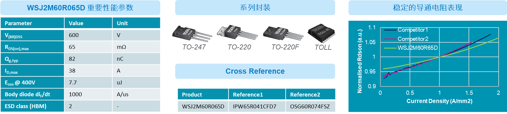
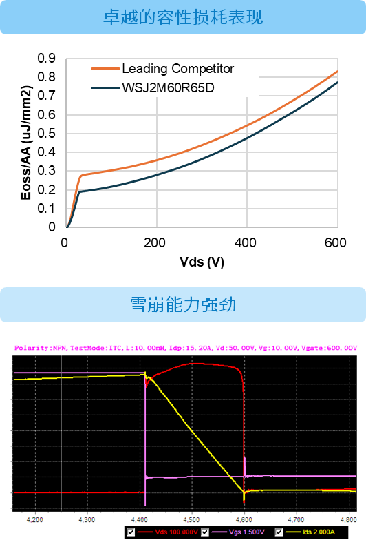
The WSJ2M60R065D is one of the flagship products in WeEn’s G2 Super Junction MOSFET lineup. Available in various packages including TO-220, TO-220F, TO-247, and TOLL. It particularly excels in terms of on-state resistance. Compared to competitors’ products, the WSJ2M60R065D maintains more stable on-state resistance across different current densities. Within its maximum continuous current range, the resistance variation does not exceed 10%. This stability provides customers with reliable performance data. Furthermore, the WSJ2M60R065D adapts well to applications with varying power requirements, demonstrating exceptional performance across diverse and complex operating environments.
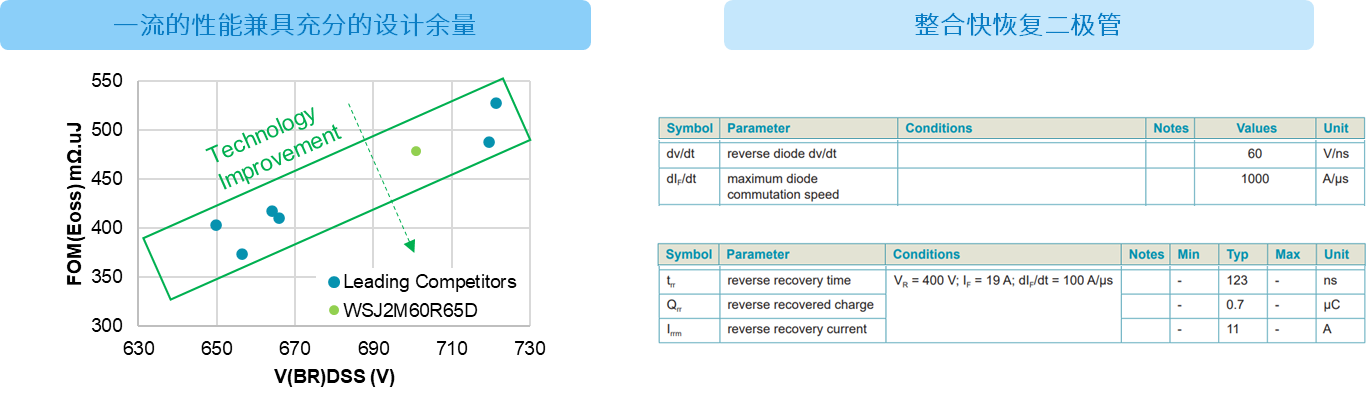
WeEn’s G2 MOSFETs are at the forefront of performance, with their Figure of Merit (FOM) on par with top global competitors. While ensuring stringent yield and process control, WeEn reserves more breakdown voltage margin for customers. 600V devices approach the standards of 650V devices available on the market, thoroughly safeguarding the reliability of customer applications. Moreover, the G2 MOSFET integrates a finely tuned fast recovery body diode, with a reverse recovery time (Trr) of only 123 ns. The body diode can withstand a commutation speed of 1000 A/μs without damage. This makes the WSJ2M60R065D particularly suitable for Zero Voltage Switching (ZVS) applications in soft-switching topologies, delivering high efficiency while handling irregular operating conditions.
However, the WSJ2M60R065D is not limited to soft-switching applications. It also demonstrates excellent performance in hard-switching applications. The WSJ2M60R065D offers significant advantages in terms of lower capacitive losses (Eoss) compared to top competitors. Additionally, its normalized ruggedness is significantly higher than the industry standard, enabling it to withstand higher overvoltage and oscillation. It also demonstrates stable and safe performance in hard-switching topologies such as Power Factor Correction (PFC) circuits.
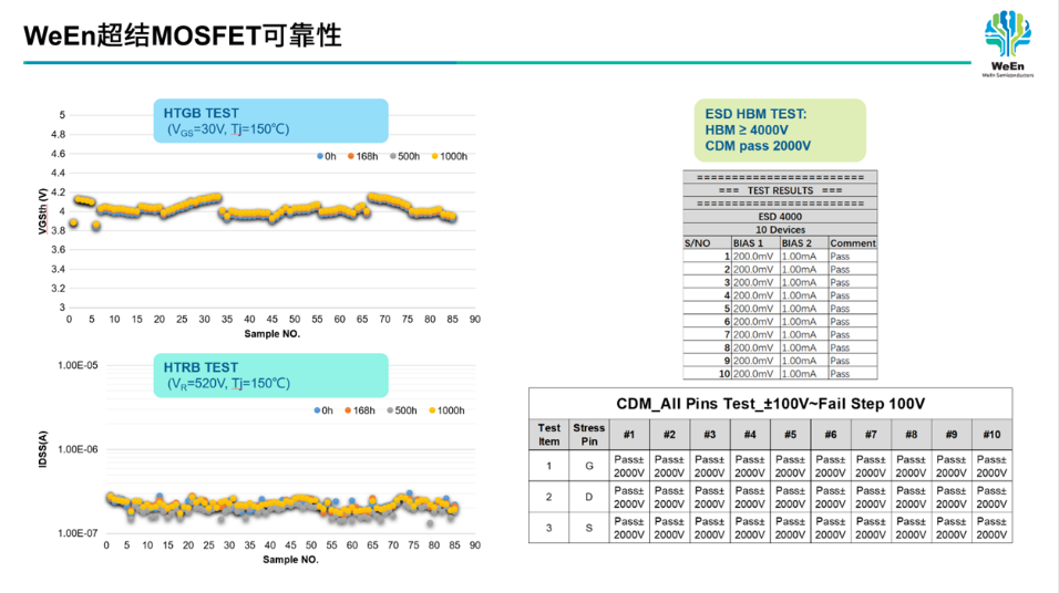
WeEn consistently adheres to rigorous and reliable quality assessment practices. In accelerated aging tests, the company maintains a zero-tolerance policy for product failures. WeEn MOSFET products demonstrate excellent consistency in performance during high-temperature stress aging tests at 168, 500, and 1000 hours. Furthermore, WeEn conducts additional reviews of the ESD (Electrostatic Discharge) capability of the device to minimize quality issues during production, packaging, and transportation. The WSJ2M60R065D demonstrates a robust quality level with a CDM (Charged Device Model) capability exceeding 2000V and an HBM (Human Body Model) capability of over 4000V.
Original – WeEn Semiconductors
