-
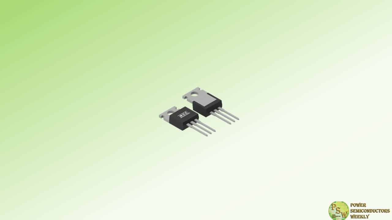
MCC Semi is unleashing the ultimate component for high-power switching — 100V N-Channel MOSFET, MCP2D6N10Y. Leveraging advanced split-gate-trench (SGT) technology and low on-resistance of 2.6mΩ, this MOSFET is made to slash conduction losses while enhancing thermal efficiency.
Demanding power electronics get an extra boost of efficiency from its ultra-low junction-to-case thermal resistance of 0.6K/W. The TO-220 package only enhances its performance thanks to its high surge capability.
An ideal combination of robust current handling, superior heat dissipation, and optimal efficiency ensures this N-channel MOSFET delivers unwavering operation in high-power applications ranging from battery management systems and motor drives to DC-DC converters.
Features & Benefits:
- High-performance 100V N-channel MOSFET
- Utilizes SGT technology
- Low on-resistance of 2.6mΩ
- Impressive junction-to-case thermal resistance of 0.6K/W
- Maximizes thermal efficiency and minimizes power losses
- Excellent thermal capabilities
- Robust current handling capacity
- Designed for TO-220 package with high surge capability
Original – Micro Commercial Components
-

Maspower Semiconductor announced the launch of its latest IGBT (Insulated Gate Bipolar Transistor) module, the MSG140T120HLF4. This advanced device is designed to meet the rigorous demands of high-power applications, including electric vehicle (EV) charging, string converters, industrial uninterruptible power supplies (UPS), and other power-train systems requiring high-efficiency power switching.
Features and Specifications
The MSG140T120HLF4 boasts a remarkable set of features that make it an ideal choice for high-voltage and high-current applications.
- High Voltage and Current Capability: With a collector-emitter voltage (VCE) of up to 1200V and a continuous collector current (IC) of 140A at 100°C, this IGBT module can handle demanding power loads with ease.
- Very Low Saturation Voltage: The device offers an ultra-low saturation voltage (VCE(sat)) of just 1.94V at 100A, ensuring high efficiency in power conversion.
- High Thermal Tolerance: The maximum junction temperature (TJ) is rated at 175°C, allowing for operation in harsh environments without compromising performance.
- Positive Temperature Coefficient: The device exhibits a positive temperature coefficient, improving thermal stability and reducing the risk of thermal runaway.
- Fast Switching Speeds: With rapid turn-on and turn-off delays, rise times, and fall times, the IGBT module ensures high-speed switching for efficient power conversion.
- High Power Handling: With a maximum collector current of 280A at 25°C and 140A at 100°C, this IGBT module can effortlessly handle high-current demands.
- Tight Parameter Distribution: Ensures consistent performance across multiple units, simplifying design and manufacturing processes.
- High Input Impedance: Minimizes gate drive requirements, reducing system complexity and cost.
Versatile Applications
With its exceptional electrical and thermal performance, the MSG140T120HLF4 is well-suited for a wide range of applications that require high-power switching capabilities.
- Electric Vehicle (EV) Charging: Its high power handling capability and fast switching speeds make it ideal for EV charging stations.
- String Converters: Suitable for solar and other renewable energy systems requiring efficient power conversion and efficient energy management.
- Industrial UPS Systems: Ensures uninterrupted power supply to critical industrial equipment, minimizing downtime and maintaining operational continuity.
- Other High-Power Train Applications: Suitable for a variety of high-power switching applications, including motor drives, inverters, and power conversion systems.
Original – Maspower Semiconductor
-

onsemi announced results for the second quarter of 2024 with the following highlights:
- Revenue of $1,735.2 million
- GAAP gross margin and non-GAAP gross margin of 45.2% and 45.3%, respectively
- GAAP operating margin and non-GAAP operating margin of 22.4% and 27.5%, respectively
- GAAP diluted earnings per share and non-GAAP diluted earnings per share of $0.78 and $0.96, respectively
- Returned ~$650 million of free cash flow over last twelve months to shareholders through stock repurchases
“We remain dedicated to driving growth through market share gains, doubling down on investments in strategic markets, and expanding the breadth of our portfolio of industry-leading products with analog and mixed-signal solutions,” said Hassane El-Khoury, president and CEO, onsemi. “As reflected by our recent supply agreement with Volkswagen Group, we also continue to strengthen our silicon carbide leadership position in automotive as we ramp production with leading global OEMs in Europe, North America and China.”
Original – onsemi
-

VisIC Technologies Ltd. has partnered with Heraeus Electronics and PINK to develop an advanced power module utilizing D3GaN technology. This groundbreaking power module is based on a silicon nitride (Si₃N₄) ceramic substrate, an innovative silver (Ag) sintering process and advanced top side interconnect, promising unprecedented reliability and performance for battery electric vehicles (BEVs).
The collaboration brings together VisIC’s expertise in GaN-based devices, Heraeus Electronics’ cutting-edge packaging materials know-how, and PINK’s state-of-the-art sintering technology. The synergy of these industry leaders has culminated in the development of a power module that is setting new standards for GaN based power modules to revolutionize the EV industry.
VisIC’s D3GaN technology is at the heart of this power module, offering significant improvements in efficiency, thermal management, and power density. This technology leverages the superior electrical properties of gallium nitride to deliver faster switching speeds and higher power handling capabilities compared to traditional silicon-based devices.
The use of a Si₃N₄ metal ceramic substrate is a key innovation in this power module. Si₃N₄ is known for its excellent thermal conductivity, mechanical strength, and reliability under high-temperature conditions. These properties are crucial for the demanding environment of electric vehicle applications, ensuring the power module can withstand the rigors of everyday use while maintaining optimal performance.
The adoption of the silver sintering process by PINK enhances the thermal and electrical conductivity of the module. Silver sintering is a low-temperature bonding process that creates robust and reliable connections between components, improving the module’s overall durability and efficiency. This process is critical for the high reliability required in EV powertrains, where consistent performance is non-negotiable.
The resulting power module is designed to meet the stringent reliability and performance standards of the electric vehicle industry. Its advanced materials and innovative construction techniques ensure it can deliver the high-power density of over 500Arms/650V and efficiency needed for modern BEVs, while also offering long-term reliability and durability at a cost point near silicon devices.
This collaboration marks a significant milestone in the advancement of power electronics for electric vehicles. The integration of VisIC’s D3GaN technology with Heraeus Electronics’ sintering paste and PINK’s Ag and Cu sintering process and flexible sintering equipment sets a new benchmark for power module performance in the EV market. This innovation is expected to drive the adoption of GaN technology in EV applications, paving the way for more efficient, reliable, and sustainable electric transportation solutions.
Tamara Baksht, CEO of VisIC, state: “We are thrilled to work with the leading manufacturer of sintering processes of Heraeus Electronics and PINK and adapt their experience into GaN based power modules to develop the next generation of power module for high volume automotive inverter applications.”
PINK, Andrea Pink, CEO of PINK statement: “We are excited to work with such a future driven company as VisIC together with our long-term partner Heraeus Electronics, supporting the newest product innovation for GaN applications.”
Heraeus Electronics Dr. Michael Jörger, EVP Head of Business Line Power Electronic Materials added: “With our materials, application know-how and engineering services we are glad to work with our partners on speeding up the innovative approach of highly efficient GaN modules for automotive applications.”
Original – VisIC Technologies
-

Toshiba Electronic Devices & Storage Corporation and Toshiba Corporation (Toshiba Group) have developed technology that mitigates the parasitic oscillation that occurs during switching operations by power modules with silicon carbide (SiC) MOSFETs connected in parallel, even with a 60% smaller gate resistance than is typical. The technology reduces power loss in power modules, mitigates oscillation, and realizes highly reliable switching operations.
The drive for carbon neutrality is stimulating demand for technologies that improve energy efficiency in many areas, including renewables, railways, and industrial equipment. In these sectors, the application of power modules built around SiC MOSFETs is seen as a solution that supports high-speed switching at high voltages and large currents—which is particularly important for the miniaturization of power converters, where higher switching frequencies result in higher rates of switching losses against power consumption.
Connecting multiple chips in parallel in power modules can form oscillation circuits, the result of wiring inductance between the chips and their parasitic capacitance. It can reduce module reliability if not countered, which is usually done by increasing gate resistance. However, this approach slows switching speed, resulting in a trade-off with switching losses. For power modules with SiC MOSFETs to perform high-speed switching, another approach is needed.
Toshiba Group used an equivalent circuit model of the power module (Figure 1) to determine the theoretical condition that triggers parasitic oscillation, and developed a wiring layout less likely to cause it. This was done by analyzing simulations of parasitic oscillation occurs when Lg/Ls, the ratio of gate-to-gate inductance Lg and source-to-source inductance Ls of parallel chips, is below a certain value (Figure 2). As increasing Lg/Ls is an effective means of mitigating parasitic oscillation, Toshiba Group fabricated prototype modules with different Lg/Ls and measured switching. This confirmed that increasing Lg/Ls mitigated oscillation, even with a 60% smaller gate resistance than that required by the alternative approach of increasing gate resistance (Figure 3).
Applying this approach to oscillation mitigation in power modules now under development has realized a power module less likely to cause parasitic oscillation, even with minimal gate resistance, that achieves low power loss with mitigated oscillation, and delivers highly reliable switching operation. Toshiba Group will continue to make refine the modules toward an early product launch.
Toshiba Group presented the details of this technology on June 6 at the 36th International Symposium on Power Semiconductor Devices and ICs (ISPSD) 2024, an international power semiconductor conference held in Bremen, Germany from June 2 to 6.
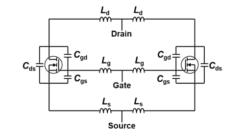
Figure 1. Model equivalent circuit of two MOSFETs connected in parallel 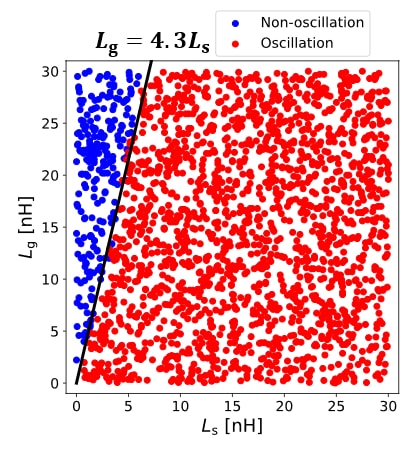
Figure 2. Simulation of oscillation in two MOSFETs with zero gate resistance connected in parallel 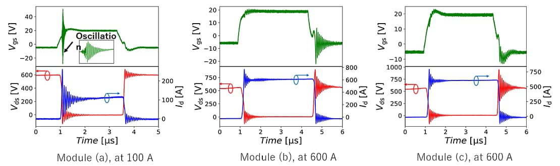
Vgs: Gate-Source voltage, Vds: Drain-Source voltage, Id: Drain current
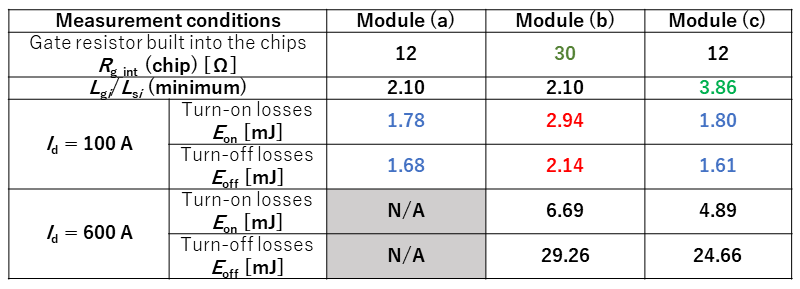
Figure 3. Switching waveforms and switching losses of the prototype modules (Source: Toshiba Group tests) Original – Toshiba
-

Infineon Technologies AG expanded the lawsuit pending before the District Court for the Northern District of California on 23 July 2024, adding claims against Innoscience (Zhuhai) Technology Company, Ltd., and Innoscience America, Inc. and affiliates based on the infringement of three additional patents referring to gallium nitride (GaN) technology owned by Infineon. In addition, Infineon today filed a complaint with the U.S. International Trade Commission (USITC) containing legal claims referring to the same four patents covered by the lawsuit.
Infineon seeks a permanent injunction for the infringement of United States patents referring to gallium nitride (GaN) technology owned by Infineon. The patent claims cover core aspects of GaN power semiconductors encompassing innovations that enable performance and reliability of Infineon’s proprietary GaN power transistors.
Already, on 14 March 2024, Infineon filed a patent infringement suit against Innoscience in the United States with the District Court for the Northern District of California. On 4 June 2024, Infineon filed a corresponding lawsuit with the District Court Munich, Germany. Additional lawsuits were filed against distributors of Innoscience in Germany.
Furthermore, Infineon successfully filed for a preliminary injunction (court order), which the District Court Munich issued on 12 June 2024. According to this court order Innoscience was obligated to remove all infringing product from their booth at the international power electronics trade show PCIM Europe.
Infineon leads the industry with its GaN patent portfolio, comprising approximately 350 patent families. Infineon’s portfolio of silicon, silicon carbide, gallium nitride power transistors and complementary drivers and controllers was enhanced with the October 2023 acquisition of GaN Systems Inc. The acquisition boosted Infineon’s GaN offering and further expanded its leading position in power semiconductors.
Original – Infineon Technologies
-

MCC introduced the latest additions to its robust portfolio: 10 1200V SiC N-channel MOSFETs in versatile TO-247-4, TO-247-4L, and TO-247AB packages. These new MOSFETs are available in 3-pin and 4-in (Kelvin source) configurations and meet the rising demand for high-power, high-voltage applications.
Boasting exceptional on-resistance values from 21mΩ to 120mΩ (typ.) and fast switching speeds, these components are the ones you can count on for reliable performance. Their excellent thermal properties and fast intrinsic body diode ensure smooth, efficient operation in the most challenging conditions, making them a must-have for critical power systems.
Features & Benefits:
- High-power capability: 1200V MOSFET with SiC technology
- Fast, reliable switching: Intrinsic body diode improves efficiency & ruggedness Enhanced performance: High switching speed with low gate charge
- Wide on-resistance selection: ranging from 21mΩ to 120mΩ (typ.)
- Efficiency: Superior thermal properties and low switching losses
- Durability: Avalanche ruggedness
- Versatility: TO247 3-pin and 4-pin package options
Original – Micro Commercial Components
-

Power Master Semiconductor (PMS) announced the release of its new AEC-Q101 qualified 1200V eSiC MOSFET in a D2PAK-7L package, designed to revolutionize power electronics in electric vehicles (EVs). PMS’s automotive-grade 1200V eSiC MOSFET offers superior efficiency, high power density, high reliability, and enables bi-directional operation, making it an ideal choice for a wide range of automotive applications, including on-board chargers (OBCs), DC-DC converters, and e-compressors.
The automotive industry is rapidly transitioning towards electrification, driven by the growing demand for sustainable and environmentally friendly transportation solutions. This shift has created a surge in demand for high-performance power electronics that can meet the stringent requirements of EV applications. Bi-directional operation is the key trend for the on-board chargers (OBCs) applications to meet V2L (Vehicle to Load), V2G (Vehicle to Grid), V2V (Vehicle to Vehicle), and V2H (Vehicle to Home appliance).
Therefore, the topology of OBCs is moving to Totem-pole PFC + CLLC or DAP resonant converter from Interleaved CCM PFC or Dual boost bridgeless PFC + LLC resonant converters. Larger battery capacity and faster charging demands are driving 800V battery systems for BEV application.
The automotive grade 1200V eSiC MOSFET is an optimized solution for the e-compressor, an indispensable power conversion system for efficient thermal management that increases battery life, charging efficiency, and driving range, and maintains a comfortable environment. It is also optimized for Totem-Pole PFC and CLLC/DAB (Dual Active Bridge) topologies, which are essential for bidirectional power conversion, a key trend in onboard chargers (OBC) for 800V battery system in electric vehicles.
Key Features of automotive grade 1200V e SiC MOSFET
- AEC-Q101 qualified for automotive applications
- Robust Avalanche Capability
- 100% Avalanche Tested
- Operating temperature range : -55°C to +175°C
- Low switching losses
- D2PAK-7L kelvin source package for ease of design and integration
“Driven by our unwavering commitment to innovation and sustainability, Power Master Semiconductor continuously develops power device solutions that achieve breakthrough efficiency and performance”, said Namjin Kim, Senior Director of Sales & Marketing.” The introduction of our new automotive-grade 1200V eSiC MOSFET represents a major leap forward in empowering the automotive industry’s shift towards cleaner, more energy-efficient power electronics. We are confident that this innovative solution will be the optimal choice for high-performance automotive applications.”
Original – Power Master Semiconductor
-

As expected, Siltronic AG’s business performance in Q2 2024 was again characterized by weak demand in the wafer market, which resulted from continued increased inventories in the chip industry. Due to the lower wafer area sold, half-year sales of EUR 694.8 million were significantly lower than in the same period of the previous year (H1 2023: EUR 808.2 million). However, at EUR 351.3 million, sales in Q2 2024 slightly exceeded the previous quarter (Q1 2024: EUR 343.5 million) by 2.3 percent.
“Q2 was in line with expectations. On a positive note, the end markets, partially driven by Artificial Intelligence, will grow this year. However, this is not yet reflected in our order situation due to still elevated inventory levels. We are pleased that we were able to slightly increase our sales in Q2 compared to the previous quarter and continued to achieve a solid EBITDA margin of 25.8 percent,” comments Dr. Michael Heckmeier, CEO of Siltronic, on the development.
Business development in H1 2024 influenced by weak demand, sales prices almost stable
In Q2 2024, Siltronic generated sales of EUR 351.3 million, up 2.3 percent on the previous quarter (Q1 2024: EUR 343.5 million) due to the increase in wafer area sold. Sales prices were almost unchanged quarter-on-quarter. Sales of EUR 694.8 million were generated in H1 2024 (H1 2023: EUR 808.2 million). The decline is primarily due to the lower sales volume. Price and currency effects had no significant impact in the half-year comparison.
On the cost side, the increase in wafer area sold and higher depreciation due to investments had a particularly noticeable impact on the quarter-on-quarter comparison. As expected, a small loss from currency hedging transactions was recognized in the other operating result in Q2.
As a result, EBITDA in Q2 2024 remained almost unchanged compared to the previous quarter at EUR 90.6 million (Q1 2024: EUR 90.8 million) despite a slight increase in sales. At 25.8 percent, the EBITDA margin remained at a solid level (Q1 2024: 26.4 percent). In a half-year comparison, EBITDA fell to EUR 181.4 million (H1 2023: EUR 243.8 million), mainly due to lower demand, and reached a margin of 26.1 percent (H1 2023: 30.2 percent).
The decline in costs due to the lower sales volume was mitigated by a lower fixed cost dilution, and a lower currency hedging result was also noticeable in the half-year comparison. In addition, H1 2024 saw an increase in depreciation and amortization.
Net profit for the period fell from EUR 27.7 million in Q1 2024 to EUR 22.4 million in Q2 and from EUR 133.9 million in H1 2023 to EUR 50.1 million in H1 2024. In addition to the effects described above, a lower financial result due to investments contributed to the reduction. Earnings per share amounted to EUR 0.73 in Q2 2024 and EUR 1.59 in H1 2024.
Net assets and financial position still affected by high investments
With an equity ratio of 46.5 percent as of June 30, 2024, Siltronic continues to have a good balance sheet quality (December 31, 2023: 46.6 percent). Cash and cash equivalents and short-term financial investments fell by EUR 129.5 million to EUR 327.4 million in H1 2024.
This was due to net payments for investments of EUR 411.2 million with a focus on the new 300 mm fab in Singapore and the dividend payment of EUR 36.0 million to Siltronic AG’s shareholders. In the same period, these payments were opposed by cash inflows of EUR 171.4 million from operating activities and cash inflows of EUR 150.0 million from a loan that was partially drawn.
Due to the high level of investments, the net cash flow fell to EUR -252.8 million and was negative, as expected. Accordingly, net financial debt increased by a total of EUR 283.5 million to EUR 639.2 million compared to December 31, 2023.
Guidance for 2024
The Executive Board of Siltronic AG has specified its guidance published at the end of April and now expects Group sales to decline by a high single-digit percentage compared to the previous year. With a view to the financial year 2024, this is primarily due to lower volumes as well as each slightly negative exchange rate- (EUR/USD 1.10), price- and product mix effects.
The EBITDA margin is expected to be at the upper end of the previously communicated range of 23 to 25 percent. However, the EBITDA margin in H2 will not reach the level of H1. Profitability in H2 will be impacted by both slightly negative price and product mix effects as well as ramp costs for the new Singapore fab, which will start to impact earnings in Q4.
In addition, one production line is scheduled for maintenance in Q4, which will be bridged by inventory reductions and will also have a negative impact on the margin. Capex is expected to be in the range of EUR 500 million to EUR 530 million, with depreciation and amortization below EUR 300 million.
Original – Siltronic
-
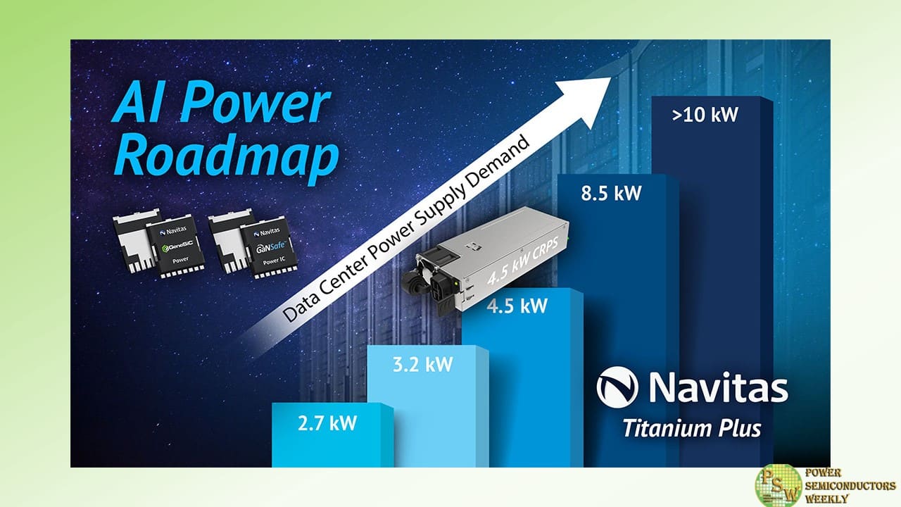
Navitas Semiconductor released its 4.5 kW AI data center power supply reference design, with optimized GaNSafe™ and Gen-3 ‘Fast’ (G3F) SiC power components. The optimized design enables the world’s highest power density with 137 W/in3 and over 97% efficiency.
Next-generation AI GPUs like NVIDIA’s Blackwell B100 and B200 each demand over 1 kW of power for high-power computation, 3x higher than traditional CPUs. These new demands are driving power-per-rack specifications from 30-40 kW up to 100 kW.
Navitas announced its AI Power Roadmap in March 2024, showcasing next-generation data center power solutions for the growing demand in AI and high-performance computing (HPC) systems. The first design was a GaNFast-based 3.2 kW AC-DC converter in the Common Redundant Power Supply (CRPS) form factor, as defined by the hyperscale Open Compute Project. The 3.2 kW CRPS185 (for 185 mm length) enabled a 40% size reduction vs. the equivalent legacy silicon approach and easily exceeded the ‘Titanium Plus’ efficiency benchmark, critical for data center operating models and a requirement for European data center regulations.
Now, the latest 4.5 kW CRPS185 design demonstrates how new GaNSafe™ power ICs and GeneSiC Gen-3 ‘Fast’ (G3F) MOSFETs enables the world’s highest power density and efficiency solution. At the heart of the design is an interleaved CCM totem-pole PFC using SiC with full-bridge LLC topology with GaN, where the fundamental strengths of each semiconductor technology are exploited for the highest frequency, coolest operation, optimized reliability and robustness, and highest power density and efficiency. The 650 V G3F SiC MOSFETs feature ‘trench-assisted planar’ technology which delivers world-leading performance over temperature for the highest system efficiency and reliability in real-world applications.
For the LLC stage, 650 V GaNSafe power ICs are ideal and unique in the industry with integrated power, protection, control, and drive in an easy-to-use, robust, thermally-adept TOLL power package. Additionally, GaNSafe power ICs offer extremely low switching losses, with a transient-voltage capability up to 800 V, and other high-speed advantages such as low gate charge (Qg), output capacitance (COSS), and no reverse-recovery loss (Qrr). High-speed switching reduces the size, weight, and cost of passive components in a power supply, such as transformers, capacitors, and EMI filters. As power density increases, next-gen GaN and SiC enable sustainability benefits, specifically CO2 reductions due to system efficiency increases and ‘dematerialization’.
The 3.2 kW and 4.5 kW platforms have already generated significant market interest with over 30 data center customer projects in development expected to drive millions in GaN and SiC revenue, ramping from 2024 into 2025.
Navitas’ AI data center power supply reference designs dramatically accelerate customer developments, minimize time-to-market, and set new industry benchmarks in energy efficiency, power density and system cost, enabled by GaNFast power ICs and GeneSiC MOSFETs. These system platforms include complete design collateral with fully tested hardware, embedded software, schematics, bills-of-material, layout, simulation, and hardware test results.
“AI is dramatically accelerating power requirements of data centers, processors and anywhere AI is going in the decades to come creating a significant challenge for our industry. Our system design center has stepped up to this challenge delivering a 3x increase in power in less than 18 months”, said Gene Sheridan, CEO of Navitas Semiconductor. “Our latest GaNFast technology, combined with our G3F SiC technology are delivering the highest power density and efficiency the world has ever seen…the perfect solution for the Blackwell AI processors and beyond.”
Original – Navitas Semiconductor
