-

Navitas Semiconductor announced that Dr. Ranbir Singh, formerly Executive Vice President at Navitas and the founder and CEO of GeneSiC Semiconductor, has been appointed to Navitas’ board of directors.
“We are pleased to welcome Ranbir to the board of directors,” said Gene Sheridan, Chairman, President and CEO. “Ranbir has led the industry with over 30 years of SiC innovation as the founder and CEO of GeneSiC; and 8 years prior to that at Wolfspeed (formerly Cree, Inc.) and brings deep industry knowledge to the board. We look forward to his contributions as we grow our business with next-generation, clean-energy power for an efficient and sustainable future.”
Dr. Singh joined Navitas with the acquisition of GeneSiC Semiconductor, which he founded in 2004. Dr. Singh has dedicated his life to the mission of high-performance, high-reliability silicon carbide technology, and is highly respected in the power electronics community, with several awards, over 200 journal and conference papers, a book and over 40 US patents.
“I am excited to be joining the Navitas board at this pivotal moment as the company leads technical innovation with disruptive, wide band-gap technology, into fast-growing AI, EV and Mobile markets,” said Dr. Singh. “Navitas is executing a significant transformation in the semiconductor industry, and it is an honor to have the opportunity to continue to contribute to the company’s growth and innovation.”
Dr. Singh holds a Bachelor of Technology, Electrical Engineering from the Indian Institute of Technology, Delhi, and both Master’s and PhD in Electrical Engineering – Power Semiconductors, from North Carolina State University (NCSU), Raleigh. He was inducted into NCSU’s Department of Electrical and Computer Engineering (ECE) Alumni Hall of Fame in 2022.
Original – Navitas Semiconductor
-

The U.S. Department of Commerce’s Bureau of Industry and Security (BIS) announced a package of rules designed to further impair the People’s Republic of China’s (PRC) capability to produce advanced-node semiconductors that can be used in the next generation of advanced weapon systems and in artificial intelligence (AI) and advanced computing, which have significant military applications. This action is a proactive measure enhancing the Department of Commerce’s work to impede the PRC’s ability to procure and produce the technologies necessary for its military modernization.
The rules include new controls on 24 types of semiconductor manufacturing equipment and 3 types of software tools for developing or producing semiconductors; new controls on high-bandwidth memory (HBM); new red flag guidance to address compliance and diversion concerns; 140 Entity List additions and 14 modifications spanning PRC tool manufacturers, semiconductor fabs, and investment companies involved in advancing the PRC government’s military modernization; and several critical regulatory changes to enhance the effectiveness of our previous controls.
“This action is the culmination of the Biden-Harris Administration’s targeted approach, in concert with our allies and partners, to impair the PRC’s ability to indigenize the production of advanced technologies that pose a risk to our national security,” said U.S. Secretary of Commerce Gina Raimondo. “Further strengthening our export controls underscores the central role of the Department of Commerce in executing the United States’ broader national security strategy. No Administration has been tougher in strategically addressing China’s military modernization through export controls than the Biden-Harris Administration.”
“The United States has taken significant steps to protect our technology from being used by our adversaries in ways that threaten our national security. As technology evolves, and our adversaries seek new ways to evade restrictions, we will continue to work with our allies and partners to proactively and aggressively safeguard our world-leading technologies and know-how so they aren’t used to undermine our national security,” said National Security Advisor Jake Sullivan.
“This action builds on BIS’s laser-focused work, undertaken over the past few years, to impose strategic controls that have hindered the PRC’s ability to produce advanced semiconductors and AI capabilities directly impacting U.S. national security. We are constantly talking to our allies and partners as well as reassessing and updating our controls. Today’s announcement represents the next step in that ongoing work,” said Under Secretary of Commerce for Industry and Security Alan Estevez. “This package is proactive and innovative in how we are responding to increasingly sophisticated actors and complex supply chains. We must ensure that we stay ahead of the PRC by protecting our advanced technology.”
“The PRC’s Military-Civil Fusion strategy presents a significant risk that advanced node semiconductors will be used in military applications that threaten the security of the United States, as well as the security of our allies and partners,” said Assistant Secretary of Commerce for Export Administration Thea D. Rozman Kendler. “These rules build on previous actions taken in service of our longstanding goal: protecting our collective security by constraining the PRC’s ability to indigenize the most advanced technologies, without unduly interfering with the continuing trade of technology.”
“The purpose of these Entity List actions is to stop PRC companies from leveraging U.S. technology to indigenously produce advanced semiconductors,” said Matthew S. Axelrod, Assistant Secretary for Export Enforcement. “By adding key semiconductor fabrication facilities, equipment manufacturers, and investment companies to the Entity List, we are directly impeding the PRC’s military modernization, WMD programs, and ability to repress human rights.”
Taking Novel Approaches to Impair and Impede the PRC’s Military Modernization
Throughout the Biden-Harris Administration, in coordination with U.S. allies and partners, BIS has taken novel approaches to address an ever-changing geopolitical and technological landscape and respond to increasingly sophisticated threat actors.
All of the policy changes announced today are designed to limit the PRC’s ability to indigenize the production of advanced technologies – such as advanced-node integrated circuits and the equipment used to produce them – that pose a substantial risk to U.S. national security. The semiconductor manufacturing equipment controlled by today’s rules is needed to produce advanced-node integrated circuits, which are necessary for advanced weapon systems and advanced AI used in military applications.
Advancements in large-scale AI models have shown striking performance improvements across many human abilities and may be used in advanced military and intelligence applications. These models have the ability to rapidly review and synthesize large amounts of information into actionable points. Advanced AI models could be used for rapid response scenarios on the battlefield; lowering the barrier to develop cyberweapons or chemical, biological, radiological, or nuclear weapons; and utilizing facial and voice recognition to repress and surveil minorities and political dissidents.
This announcement underscores the United States’ “small yard, high fence” strategy and will restrict the PRC’s ability to produce technologies key to its military modernization or repression of human rights.
These actions serve two primary objectives:
- Slowing the PRC’s development of advanced AI that has the potential to change the future of warfare; and
- Impairing the PRC’s development of an indigenous semiconductor ecosystem – an ecosystem built at the expense of U.S. and allied national security.
In line with these objectives, BIS is implementing several regulatory measures, including but not limited to:
- New controls on semiconductor manufacturing equipment needed to produce advanced-node integrated circuits, including certain etch, deposition, lithography, ion implantation, annealing, metrology and inspection, and cleaning tools.
- New controls on software tools for developing or producing advanced-node integrated circuits, including certain software that increases the productivity of advanced machines or allows less-advanced machines to produce advanced chips.
- New controls on high-bandwidth memory (HBM). HBM is critical to both AI training and inference at scale and is a key component of advanced computing integrated circuits (ICs). The new controls apply to U.S.-origin HBM as well as foreign-produced HBM subject to the EAR under the advanced computing Foreign Direct Product (FDP) rule. Certain HBM will be eligible for authorization under new License Exception HBM.
- Addition of 140 entities to the Entity List, in addition to 14 modifications, including semiconductor fabs, tool companies, and investment companies that are acting at the behest of Beijing to further the PRC’s advanced chip goals which pose a risk to U.S. and allied national security.
- Establishment of two new Foreign Direct Product (FDP) rules and corresponding de minimis provisions:
- Semiconductor Manufacturing Equipment (SME) FDP: Extends jurisdiction over specified foreign-produced SME and related items if there is “knowledge” that the foreign-produced commodity is destined to Macau or a destination in Country Group D:5, including the PRC
- Footnote 5 (FN5) FDP: Extends jurisdiction over specified foreign-produced SME and related items if there is “knowledge” of certain involvement by an entity on or added to the Entity List with a FN5 designation. Such entities are being designated on the Entity List for specific national security or foreign policy concerns described in the Entity List companion rule, such as these entities’ involvement in supporting the PRC’s military modernization through the PRC’s attempts to produce advanced-node semiconductors, including for military end-uses.
- De minimis: Extends jurisdiction over specified foreign-produced SME and related items described in the above FDP rules that contain any amount of U.S.-origin integrated circuits.
- New software and technology controls, including restrictions on Electronic Computer Aided Design (ECAD) and Technology Computer Aided Design (TCAD) software and technology when there is “knowledge” that such items will be used for the design of advanced-node integrated circuits to be produced in Macau or a destination in Country Group D:5.
- Clarification to the EAR regarding existing controls on software keys. Export controls now apply to the export, reexport, or transfer (in-country) of software keys that allow access to the use of specific hardware or software or renewal of existing software and hardware use licenses.
In October 2022, BIS published an interim final rule (IFR) to restrict the PRC’s ability to both purchase and manufacture certain high-end semiconductors critical for military applications. As part of BIS’s commitment to continually evaluating the effectiveness of export controls, it released updated rules in October 2023 and April 2024. Today’s rules build on those efforts.
Original – Bureau of Industry and Security
-

Power Master Semiconductor has announced the expansion of its e SiC MOSFET family with introduction of new AEC-Q101 qualified, high-performance top-side cooling packages. These include the TSPAK DBC version and LF version, specially designed for automotive and industrial applications.
The TSPAK offers superior thermal performance, high efficiency, power density and reliability, making it ideal for a variety of automotive applications such as on-board chargers (OBCs), DC-DC converters, and e-compressors. This innovative packaging leverages Power Master Semiconductor’s latest generation of 1200V eSiC MOSFET (Gen2), employing cutting-edge technology to decouple a trade-off between specific on-resistance (Rsp) and short-circuit withstand time (SCWT). Compared to the previous generation, the new 1200V eSiC MOSFETs deliver 20% reduction in RDS(ON) and a 15% improvement in SCWT, as well as a 45% reduction in switching losses.
Key Features and Benefits of TSPAK
TSPAK LF version
- Top-side cooling package with an exposed drain at the surface, allowing direct heat dissipation to the heatsink.
- Offers superior thermal performance and supports high current capabilities.
- High temperature capability : Tj (max)= 175°C
TSPAK DBC version
- Integrates an isolated DBC ceramic pad on the surface, providing premium thermal performance and enhanced design flexibility.
- Features 3.6kV isolation voltage, extended creepage distance (5.23mm), and flexible mounting by directly connected to an external heatsink with thermal grease.
- High temperature capability : Tj (max)= 175°C
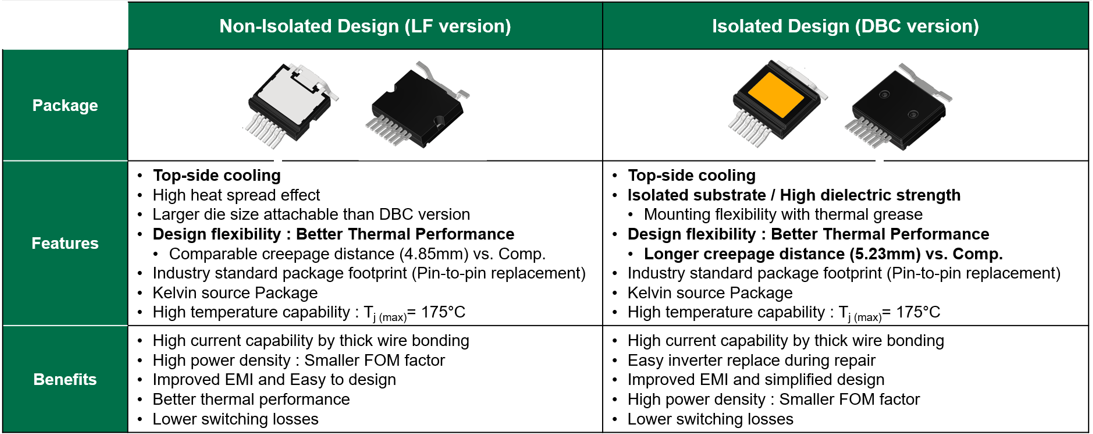
With an industry-standard footprint of 14mm x 18.58mm, the TSPAK packages provide superior thermal performance and Kelvin source configuration to minimizes gate noise and reduces turn-on losses by 60%, enabling higher-frequency operation and improved power density.
The PCR120N40M2A (LF version) and PCRZ120N40M2A (DBC version) are automotive-grade 1200V/40mΩ eSiC MOSFETs in TSPAK packages, leveraging Power Master Semiconductor’s 2nd-generation eSiC MOSFET technology to deliver optimized performance for the automotive systems.
- E-compressors, vital for efficient thermal management, extended battery life, enhanced charging efficiency, and improved driving range.
- Totem-Pole PFC and CLLC/DAB (Dual Active Bridge) topologies, essential for bidirectional power conversion in 800V battery systems used in electric vehicles.
“Cooling is one of the greatest challenges in high power design and successfully addressing it is the key enabler to reducing size and weight, which is critical in modern automotive design” said Namjin Kim, Senior Director of Sales & Marketing. “Our new top-side cooling package offer better system efficiency and minimize heat thermal path on the PCB, the system design will be simplified and compacted. We are confident that this innovative solution will be the optimal choice for high-performance automotive applications.”
“Efficient cooling is a critical challenge for reducing size and weight of high-power automotive systems,” said Namjin Kim, Senior Director of Sales & Marketing. “Our new top-side cooling package enhances system efficiency and minimizes the thermal path on the PCB, enabling simpler, more compact system designs. We believe this innovative solution will drive the high performance automotive applications.”
Original – Power Master Semiconductor
-

DENSO Corporation and Fuji Electric Co., Ltd. announced that a semiconductor supply plan submitted jointly by the companies has been approved by the Ministry of Economy, Trade and Industry. Under this plan, the companies will take part in joint investment and production of silicon carbide (SiC) power semiconductors to develop and strengthen frameworks for the supply of said semiconductors.
Power semiconductors are vital to the efficient supply of electric power. Demand for power semiconductors has been rising rapidly given that they are used in electrified vehicles, which are being adopted at an accelerated pace amid the push for the decarbonization of society. In comparison to prior silicon semiconductors, SiC power semiconductors are able to deliver superior performance under high temperature, high-frequency, and high-voltage conditions.
These devices are therefore anticipated to make large contributions to reductions in power loses as well as to more compact and lighter-weight designs for battery electric vehicle systems and other power electronics. Accordingly, growth in demand is projected for SiC power semiconductors.
In response to electrification trends, DENSO has advanced SiC technology development projects targeting increased quality and efficiency in relation to everything from wafers and element devices to modules and inverters. Meanwhile, Fuji Electric has constructed extensive frameworks encompassing all tasks spanning from the development of SiC power semiconductor elements that enable increased efficiency and more compact designs for power electronics equipment to mass production of the related modules.
Based on the approved plan, these companies will combine their respective automotive product development and production technology capabilities in a joint effort to expand their capacity for the efficient and stable supply of SiC power semiconductors throughout Japan.
Through this partnership, the companies will contribute to the development of semiconductor supply frameworks within Japan and to the improvement of the international competitiveness of Japan’s domestic semiconductor and automotive industries. In addition, this partnership is anticipated to help advance the decarbonization of society.
Original – Fuji Electric
-

Infineon Technologies AG has won the German Sustainability Award in the “Electrical Engineering and Electronics” category. “The jury is of the opinion that Infineon has assumed a leading role in the field of sustainability and serves the sector as a ‘beacon’ for successful transformation,” the judges said in their statement. The German Sustainability Award recognizes companies which make effective and exemplary contributions to transformation and which function as role models within their industry.
“We are particularly honored and delighted to win the German Sustainability Award,” said Elke Reichart, Member of the Management Board and Chief Digital and Sustainability Officer at Infineon, who accepted the award in Duesseldorf. “We at Infineon work hard to drive decarbonization and digitalization and to create a more sustainable future. This award is recognition, as well as an incentive to be a role model in sustainability and to continue rigorously implementing our ambitious sustainability strategy – together with our employees, customers and partners.”
Infineon is pursuing a comprehensive and ambitious decarbonization strategy. The company is making good progress towards the goal it defined in 2020: achieving climate neutrality by 2030. Since then, emissions have been reduced by more than two thirds while revenue has almost doubled. Moreover, Infineon is intensifying its collaboration along the entire supply chain. As a pioneer in its industry, Infineon this year began reporting emissions at the individual product level, referred to as the Product Carbon Footprint. The data is already available for half of all Infineon products today.
Infineon’s semiconductors are decisive in making the generation, transmission, storage and use of energy more efficient. A recent example of sustainable product innovation by Infineon is a new type of energy-saving silicon carbide (SiC) module, whose developers were nominated for the 2024 Deutscher Zukunftspreis. The solution increases the energy efficiency of existing high-performance electrical applications such as solar and wind power plants and train drives. Among other things, the module also facilitates the efficient electrification of large drives such as those found in agricultural and construction machinery, ships and aircraft. In concrete terms, a single electric locomotive equipped with the new drive system saves around 300 megawatt hours per year, which corresponds to the annual energy requirements of 100 single-family homes.
The German Sustainability Award is Europe’s largest award for ecological and social commitment. The jury of the German Sustainability Award (DNP) selected winners in 100 different sectors from among around 2000 competing companies. The German Sustainability Award works together with the German Chamber of Industry and Commerce (DIHK), WWF Germany, PwC Germany, Leuphana University Lüneburg (CSM Lüneburg) and numerous other industry associations to design and implement the competition.
Current reports on sustainability at Infineon can be found here.
Original – Infineon Technologies
-

Analog Devices, Inc. announced financial results for its fiscal fourth quarter and fiscal year 2024, which ended November 2, 2024.
“ADI’s revenue, profitability, and earnings per share all finished above our guided midpoint, underscoring continued business momentum and solid execution,” said Vincent Roche, CEO and Chair. “While unprecedented customer inventory headwinds drove a historic revenue decline during fiscal 2024, we maintained operating margins north of 40%, which is a testament to our business model’s resilience. We also continued to make strategic, long-term investments across engineering, manufacturing, and the end-to-end customer experience. As such, we enter 2025 as an even stronger enterprise, giving me the utmost confidence in our ability to drive increased value for customers and shareholders over the long term.”
“After a brief decline in overall bookings during our third quarter, orders picked up steadily throughout the fourth quarter, particularly in the Automotive end market. While macro uncertainty continues to limit the pace of our recovery, we remain cautiously optimistic for a strong growth year in fiscal 2025,” said Richard Puccio, CFO.
Performance for the Fourth Quarter and Fiscal Year 2024 (PDF)
Outlook for the First Quarter of Fiscal Year 2025
For the first quarter of fiscal 2025, we are forecasting revenue of $2.35 billion, +/- $100 million. At the midpoint of this revenue outlook, we expect reported operating margin of approximately 22.0%, +/- 130 bps, and adjusted operating margin of approximately 40.0%, +/- 100 bps. We are planning for reported EPS to be $0.80, +/- $0.10, and adjusted EPS to be $1.53, +/- $0.10.
Our first quarter fiscal 2025 outlook is based on current expectations and actual results may differ materially as a result of, among other things, the important factors discussed at the end of this release. These statements supersede all prior statements regarding our business outlook set forth in prior ADI news releases, and ADI disclaims any obligation to update these forward-looking statements.
The adjusted results and adjusted anticipated results above are financial measures presented on a non-GAAP basis. Reconciliations of these non-GAAP financial measures to their most directly comparable GAAP financial measures are provided in the financial tables included in this release. See also the “Non-GAAP Financial Information” section for additional information.
Original – Analog Devices
-

Valeo, a leading automotive technology company, and ROHM Semiconductor collaborate to propose and optimize the next generation of power modules for electric motor inverters using their combined expertise in power electronics management. As a first step, ROHM will provide its 2-in-1 Silicon Carbide (SiC) molded module TRCDRIVE pack™ to Valeo for future powertrain solutions.
Valeo is broadening access to efficient, electrified mobility across various vehicle types and markets from the smallest one (ebikes), through the mainstream (passenger cars) to the biggest one (eTrucks). By combining Valeo’s expertise in mechatronics, thermal management and software development with ROHM’s power modules, Valeo drives the power electronics solution forward, contributing to the performance, efficiency, and decarbonization of automotive systems worldwide.
Valeo and ROHM have been collaborating since 2022, initially focusing on technical exchanges aimed at improving the performance and efficiency of the motor inverter – a key component in the propulsion systems of electric vehicles (EVs) and plug-in hybrids (PHEVs). By refining power electronics, both companies aim to offer optimized cost/performance by delivering higher energy efficiency, reducing heat generation thanks to an optimized cooling and mechatronic integration, and increasing overall reliability with a SiC packaging.
“This partnership marks, for Valeo Power Division, a significant step forward in delivering advanced and high-efficient power electronics,” says Xavier DUPONT, Valeo Power Division CEO. “Together, we aim to set new industry standards for high voltage inverters and accelerate the transition towards more efficient and affordable electric mobility.”
“We are pleased to support Valeo, a renowned automotive supplier, with our power semiconductors. ROHM’s TRCDRIVE pack™ provides high power density, leading to an improved power efficiency. Together, we contribute to the development of highly efficient powertrains by fostering the collaboration with Valeo,” says Wolfram HARNACK, President ROHM Semiconductor GmbH.
These evolutions are all essential to supporting the growing demand for longer range, faster charging capabilities, and, overall a high-performance and an affordable inverter for BEVs and PHEVs.
Valeo will start supplying a first series project in early 2026. Valeo and ROHM will contribute to the improvement of efficiency and downsizing of Valeo’s next generation of xEV inverters.
Original – ROHM
-

Wolfspeed announced that Melissa Garrett has been appointed Senior Vice President and General Counsel, effective December 9, 2024. Garrett succeeds Brad Kohn, who has resigned from the company for another professional opportunity.
Garrett brings extensive legal expertise and has served as a senior member of Wolfspeed’s legal team leading global employment and non-patent litigation matters since 2015. She brings a comprehensive legal background in contracts and negotiations, litigation management, corporate governance, employment law, policy and mergers and acquisitions.
“Melissa’s contributions to Wolfspeed over the last nine years have been highly valuable, and we are pleased to welcome her to the role of General Counsel,” said Tom Werner, Executive Chairman. “With her proven track record in legal, risk and compliance, coupled with her deep institutional knowledge of Wolfspeed, she is uniquely qualified to step into this role. We deeply appreciate Brad’s tireless advocacy for Wolfspeed over the years and thank him for his dedication and many contributions to the company. He and Melissa have been working closely on all key projects, so we expect a smooth transition and we wish him all the best in his future endeavors.”
Prior to joining Wolfspeed, Garrett served as Deputy General Counsel and Assistant Corporate Secretary at Kangaroo Express. She previously served as an attorney at Jackson Lewis and Paul, Hastings, Janofsky & Walker LLP, and began her career as an attorney at Fisher & Philips. She holds a Juris Doctor from Indiana University and a Bachelor of Arts from University of Wisconsin-Madison.
Original – Wolfspeed
-

Navitas Semiconductor announced that the company’s revenue growth has been acknowledged for the third consecutive year, by Deloitte’s Technology Fast 500™. Navitas growth was driven by strong demand for its advanced, high-efficiency, wide-bandgap gallium nitride (GaN) and silicon carbide (SiC) power components, across a growing number of global markets and customers.
Now in its 30th year, the Deloitte Technology Fast 500 provides a ranking of the fastest-growing technology, media, telecommunications, life sciences, fintech, and energy tech companies — both public and private — in North America. Based on percentage fiscal year revenue growth from 2020 to 2023, Navitas achieved 571% growth as GaN and SiC technology enabled efficient, sustainable applications and displaced legacy silicon chips.
“As a ‘pure-play’, next-gen, semiconductor company, Navitas continues to outperform the overall power semiconductor market, with record sales into mobile fast chargers, now ramping AI data center revenues and a strong customer pipeline for EV opportunities,” said Gene Sheridan, CEO and co-founder. “Recent introductions like GaNSafe™, Gen-3 ‘Fast’ SiC, and a newly-announced, 48V-focused range in partnership with Infineon, have built a strong foundation for further revenue growth in applications from 20W to 20MW, and with a market opportunity of over $22B per year.”
Original – Navitas Semiconductor
-

Infineon Technologies AG introduced the EiceDRIVER™ Power 2EP1xxR family of full-bridge transformer drivers for IGBT, SiC and GaN gate driver power supplies. With the 2EP1xxR family, Infineon extends its portfolio of power devices to provide designers with a solution for isolated gate driver supply.
By using the devices, asymmetrical output voltages can be implemented to supply isolated gate drivers in a cost-effective and space-saving manner. This makes the 2EP1xxR particularly suitable for industrial or consumer applications requiring isolated gate drivers, including solar applications, electric vehicle charging, energy storage systems, welding, uninterruptible power supplies and drive applications.
The 2EP1xxR family comes in a compact TSSOP8 pin package with power integration and optimizations to generate an asymmetric output voltage. The family is optimized for asymmetric gate driver supply through its unique duty-cycle adjustment capability. The devices support a wide input voltage range up to 20 V. They also offer integrated temperature, short-circuit and undervoltage lockout (UVLO) protection to prevent unwanted system faults.
The 2EP1xxR family is available in the following four product variants: 2EP100R and 2EP101R are optimized for low component count designs for IGBT and SiC MOSFET gate driver power supplies. 2EP110R allows fine adjustment of the duty-cycle to match the output voltage ratio to the application requirements of SiC and GaN power switches. 2EP130R is optimized for highly flexible designs to meet different application requirements.
The device offers 5-stage overcurrent protection, 41 selectable switching frequencies or synchronization with external PWM for transformer matching, and 41 selectable duty-cycle options to adjust the output voltage.
Original – Infineon Technologies
