-

CVD Equipment Corporation appointed Andrew Africk to its Board of Directors. The Board of Directors also approved an expansion of the number of directors from the current level of six to seven.
“We are delighted that Mr. Africk has agreed to join our Board,” said Lawrence J. Waldman, Chairman of CVD Equipment Corporation’s Board of Directors. “We appreciate his support of the company as our largest shareholder, and we welcome his extensive corporate and financial experience that will be invaluable to our Board of Directors and executive management team.”
Mr. Africk is the founder of Searay Capital LLC, a private investment company. Mr. Africk established Searay Capital in July 2013 after 21 years leading private equity and capital markets investments for Apollo Global Management. As a Senior Partner at Apollo, Mr. Africk was responsible for investments in technology and communications, and he has 30 years of experience financing, analyzing and investing in public and private companies. Mr. Africk graduated from UCLA with a B.A. in Economics, from the University of Pennsylvania Law School with a J.D., and from the University of Pennsylvania’s Wharton School of Business with an MBA.
Manny Lakios, President and CEO of CVD Equipment Corporation, also commented, “I am very pleased to have Mr. Africk join our Board of Directors. His in-depth knowledge of the technology sector will add an additional perspective and allow him to contribute as a member of the Board of Directors strategically as we focus on key markets of high power electronics, battery materials, aerospace and industrial applications.”
Original – CVD Equipment
-
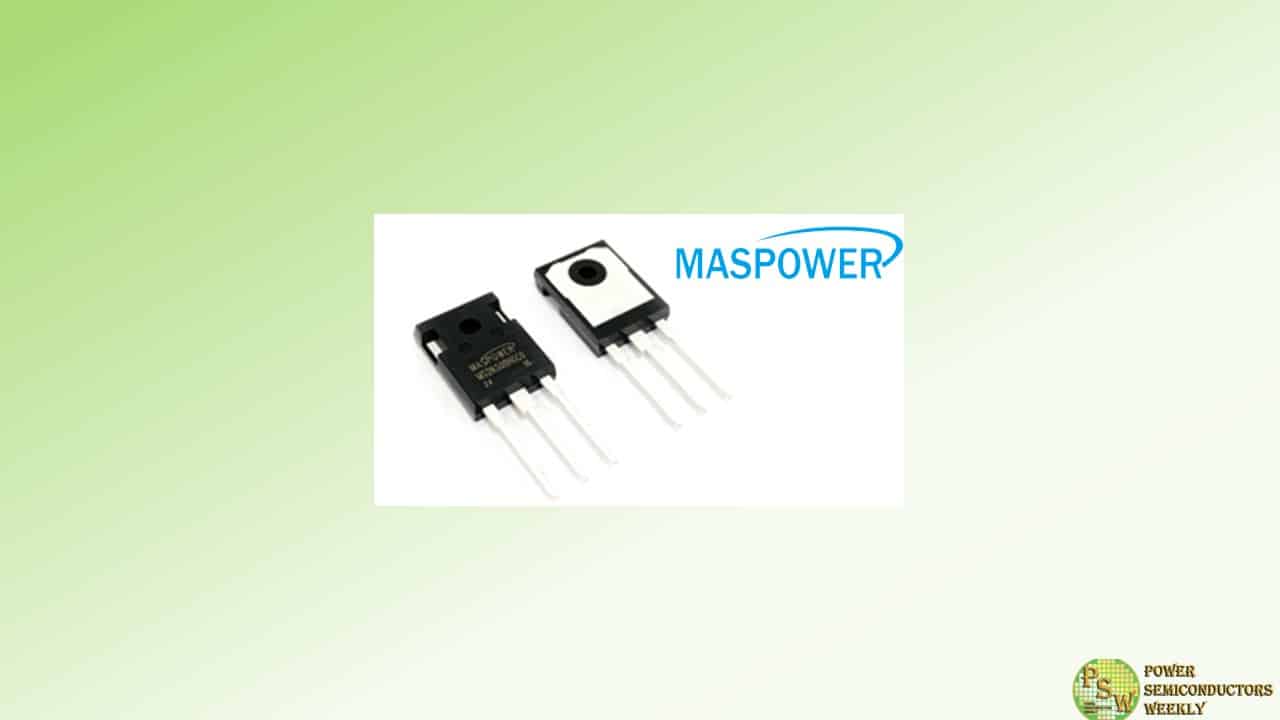
In a significant advancement for the high-voltage power electronics industry, Maspower Semiconductor has introduced the MS2N300HGC0 MOSFET, a powerful new component that sets new benchmarks in performance and reliability.
This cutting-edge product, housed in the TO-247 package, offers unprecedented performance with its robust 3000V voltage rating and 2A continuous current capability. What truly sets this MOSFET apart, however, is its rigorous testing and certification. The MS2N300HGC0 has undergone 100% avalanche testing, ensuring exceptional resilience and durability in demanding applications.
Moreover, the MS2N300HGC0’s Fast Intrinsic Diode design and minimized gate charge contribute to its high-speed switching capabilities, making it a perfect fit for high-voltage power supplies, PV inverters, switching applications and more. Its very low intrinsic capacitance further enhance its performance, delivering maximum efficiency and reliability. Maspower’s commitment to innovation and reliability is evident in the MS2N300HGC0, which has been rigorously tested and certified to meet the highest industry standards.
“The MS2N300HGC0 is a testament to our commitment to pushing the boundaries of high-voltage power electronics,” said a spokesperson from Maspower. “We are proud to offer this state-of-the-art MOSFET to our customers, enabling them to achieve unprecedented levels of performance and reliability in their applications.”
Original – Maspower Semiconductor
-

At PCIM Europe 2024, Infineon Technologies AG will showcase how its latest semiconductor, software, and tooling solutions provide answers to today’s green and digital transformation challenges. Under the motto “Driving decarbonization and digitalization. Together.”, Infineon will demonstrate the industry’s broadest power electronics portfolio covering all relevant power technologies in silicon (Si), silicon carbide (SiC), and gallium nitride (GaN).
The company will be exhibiting in a larger area this year, with the main booth #740 in Hall 7 demonstrating innovative Si and SiC-based solutions, while the adjacent booth #169 is dedicated to the broad GaN portfolio. Alternatively, visitors can also register for Infineon’s digital event platform.
Infineon’s PCIM 2024 highlights
The products, demonstrations, and design aids on display illustrate how Infineon’s product-to-system expertise in power management enables engineers to balance operational specifications with application requirements. Demonstrations will include solutions from the following areas:
- Wide-bandgap technologies: Wide-bandgap materials are revolutionizing power electronics and various applications that are driving the green and digital transformation. Infineon will demonstrate the CoolSiC™ MOSFETs 650 V and 1200 V Generation 2, which can be used to improve overall energy efficiency. Additionally, the expanded portfolio of GaN solutions will be showcased, offering a wide range of innovative packages, discrete and integrated solutions.
- Renewables, energy storage and HVDC: With its power solutions, Infineon enables the most climate-friendly forms of energy generation from wind and solar accompanied by efficient storage systems. At PCIM, the company will present a wide range of solutions for single-phase and three-phase hybrid solar inverters as well as its In-Field Power Analytics Service helping to maximize converter uptime and optimize operation in real-time.
- Industrial automation, motor drives and control: With advanced power semiconductors, Infineon is paving the way for highly reliable and energy-efficient electric motors and drive solutions in smart factories. This is achieved through a combination of efficient energy management and intelligent motor control solutions, advanced sensor functions, and reliable connectivity components. Furthermore, the company is presenting its growing range of solid-state relays and circuit breakers as well as a stack assembly solution for high-end Press Pack IGBTs.
- Information and communication technologies: True to the motto “We power AI”, Infineon exhibits innovative technologies that make it possible to meet increasing energy demands while promoting greener AI and paving the way for more efficient AI servers. This includes two-phase power supply modules, integrated point-of-load solutions, and converters. In addition, the company will showcase cutting-edge solutions, including Si, SiC, and GaN power switches, that meet the evolving needs of server technology and telecoms networks, driving efficiency, reliability, and innovation across all industries.
- eMobility, eTransportation and charging solutions: With leading power supply solutions for traction inverters, on-board chargers, DC-DC converters, and battery management systems, Infineon supports the efforts of developers and manufacturers, enabling the rapid expansion of eMobility, eTransportation, eCAV, and the corresponding charging infrastructure. Highlights presented in this area include traction inverters with fusion, single-side cooling and discrete concepts, traction inverter systems for commercial vehicles and rail transport, as well as high power fast charging solutions.
- Smart and connected homes: Infineon’s leading technology portfolio of customized, ready-to-use solutions assists manufacturers in developing innovative system designs for homes that meet the growing demand for smart, connected, and energy-efficient living solutions. Highlights in this area include USB-C charging solutions, portable battery-powered welding solutions, residential heat pumps, as well as air conditioning systems.
Infineon will also contribute to the PCIM conference program and the various forums, including a keynote by Dr. Gerald Deboy, Fellow at Infineon, on the “Challenges and Solutions to Power Latest Processor Generations for Hyper Scale Data Centers” on June 13 at 8:45 am. An overview of all contributions by Infineon experts is available at www.infineon.com/pcim.
Original – Infineon Technologies
-
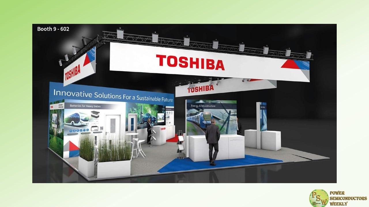
Toshiba Electronics Europe GmbH and Toshiba Materials CO., LTD. will bring solutions that support customers’ goals in reducing their CO2 footprint at the PCIM 2024 conference and exhibition (Nuremberg 11th – 13th June).
This year, the company will use the event to showcase a combination of several business units that support development of sustainable solutions. Semiconductor, battery, and fine ceramic material solutions form a complete chain of products in key applications from e-mobility, industrial, energy and infrastructure sectors.
Toshiba has manufactured top-class ceramics since the 1970s, and its pioneering Silicon Nitride substrates will be on display along with bearing balls, AMOBEADS™, and Nanocrystalline common mode choke cores.
In Toshiba’s eMobility booth area, visitors will discover demonstrations of automotive thermal management by heat pumps and fans utilising Toshiba’s newly released SmartMCD.
Toshiba’s industrial demonstrations highlight the entire product chain from control to isolation to power conversion stages, incorporating the latest generations of SiC, GaN and low-voltage MOSFET technologies. They include reference design implementations utilising modern topologies for factory automation, power supplies, and motor control applications.
Energy and infrastructure demonstrations will focus on high-power solutions such as IEGT and SiC Modules supporting voltages from 1.2kV to 3.3kV. Toshiba’s SiC Cube illustrates a solution implementation for charging infrastructure utilising SiC MOSFET devices, whereas SCiB batteries demonstrate their effective use for energy storage.
Toshiba representatives are also scheduled to participate in the conference program speeches and poster sessions on Wide Bandgap, power semiconductors and gate driver ICs topics.
Original – Toshiba
-
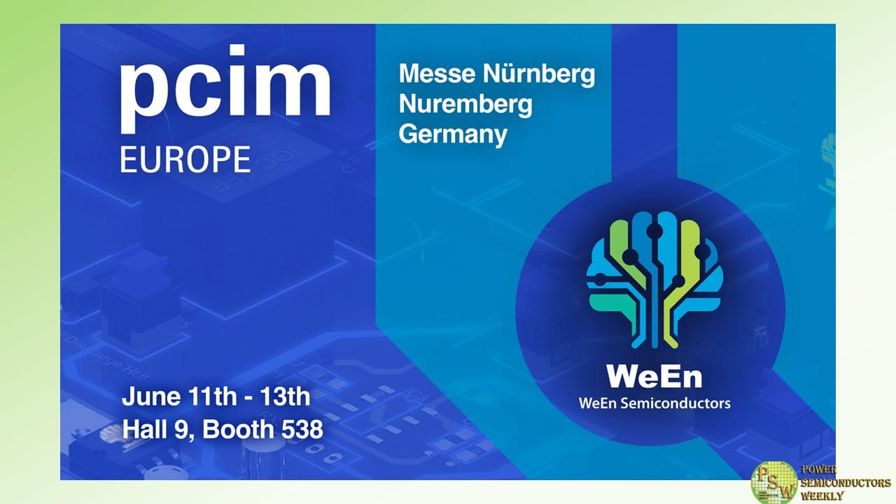
WeEn Semiconductors will be exhibiting the company’s latest highly efficient, high-power density silicon carbide (SiC) technologies, automotive grade power devices and highly reliable IGBTs at PCIM Europe 2024 in Nuremberg from June 11-13, 2024.
Established in 1979, PCIM Europe serves as a premier platform for showcasing the latest advancements in power electronics technologies and applications. This year, in Hall 9, booth 538, under the theme of ‘Power Efficiency for a Cooler Planet,’ WeEn Semiconductors will exhibit its extensive range of high-voltage 1700V SiC power modules, SiC 1200V/750V MOSFETs, Thyristors, power diodes, silicon-controlled rectifiers (SCRs), IGBTs, and other advanced power devices tailored for the renewable energy and e-mobility industries.
With a focus on efficiency, sustainability and cost reduction, WeEn’s broad portfolio offers best-in-class performance, efficiency and density for demanding applications including solar and wind power storage, electric vehicle (EV) fast chargers and traction inverters, HVAC and datacenter servers.
“At WeEn, we are dedicated to developing cost-effective power control technologies that support high voltage ratings and efficient, high-performance operation,” remarked WeEn Semiconductors CEO, Markus Mosen. “We’re excited to showcase the solutions we’ve launched in recent months at PCIM, not least those technologies targeted at renewable energy and electric mobility applications that demonstrate our commitment to products that not only meet but exceed the unique demands of every application while contributing to environmental sustainability.”
PCIM 2024 highlights
- At PCIM, WeEn is set to introduce a range of SiC MOSFETs and SiC Schottky Barrier Diodes (SBDs) in TSPAK packages for EV charging, On Board Charger (OBC), PV inverters, and high power density PSU applications. The new MOSFETs are available in 650V, 750V, 1200V, and 1700V variants, with resistance ranging from 20mΩ to 150mΩ. The current range for the new SiC SBDs is 10 to 40A in 650V, 750V, and 1200V variants.
- A range of SiC power modules in half-bridge, four-pack, six-pack, dual booster, and NPC 3L topologies will also be on display. Target markets for these SiC modules include EV charging, energy storage systems, motor drivers, industrial power supply units (PSUs), test instruments, and PV inverters.
- 1700V SiC series and 1200V / 750V auto-grade SiC MOSFETs, which encompass a diverse range of packaging options and product configurations, including surface-mount device (SMD) discrete components and top-side cooling.
- Highly reliable thyristor/diode modules, suitable for mainstream industrial applications like UPS, Inverter, soft starter, with VDRM up to 1600V and IT(RMS) up to 250A . Thanks for its planar chip technology and state-of-art module manufacture capability, those modules can be in half-bridge, parallel or antiparallel or other customized topology, it has passed 1000 hours reliability test under JEDEC standard as well 100% Pb-Free for the highest level EU RoHS compliance.
- WeEn’s product platforms include Super Junction MOSFETs with breakdown voltage ranges of 600V, 650V, and 800V. Leveraging advanced 8-inch wafer technology, WeEn offers a wide range of trench MOSFETs with voltage ranges from 20V to 30V.
- With voltage ratings from 45V to 2000V, WeEn’s Power Diodes feature current ratings from 1A to 100A. The company’s product portfolio includes low VF Schottky rectifiers, standard diodes, and ultrafast recovery rectifiers.
- WeEn’s range of IGBTs boasts extremely low leakage currents and exceptional conduction and switching characteristics at both high and low junction temperatures. They have undergone high voltage H3TRB and 100%-biased HTRB tests with a maximum junction temperature of 175°C safely. These application-specific IGBTs have been tuned to match the precise needs of each application, including switching behaviors, conduction losses, short circuit capabilities, environmental ruggedness, and freewheeling diode characterization. The 1200V and 650V variant current products, including bare dies, discrete components, and PIMs, are offered to various end customers.
Original – WeEn Semiconductors
-
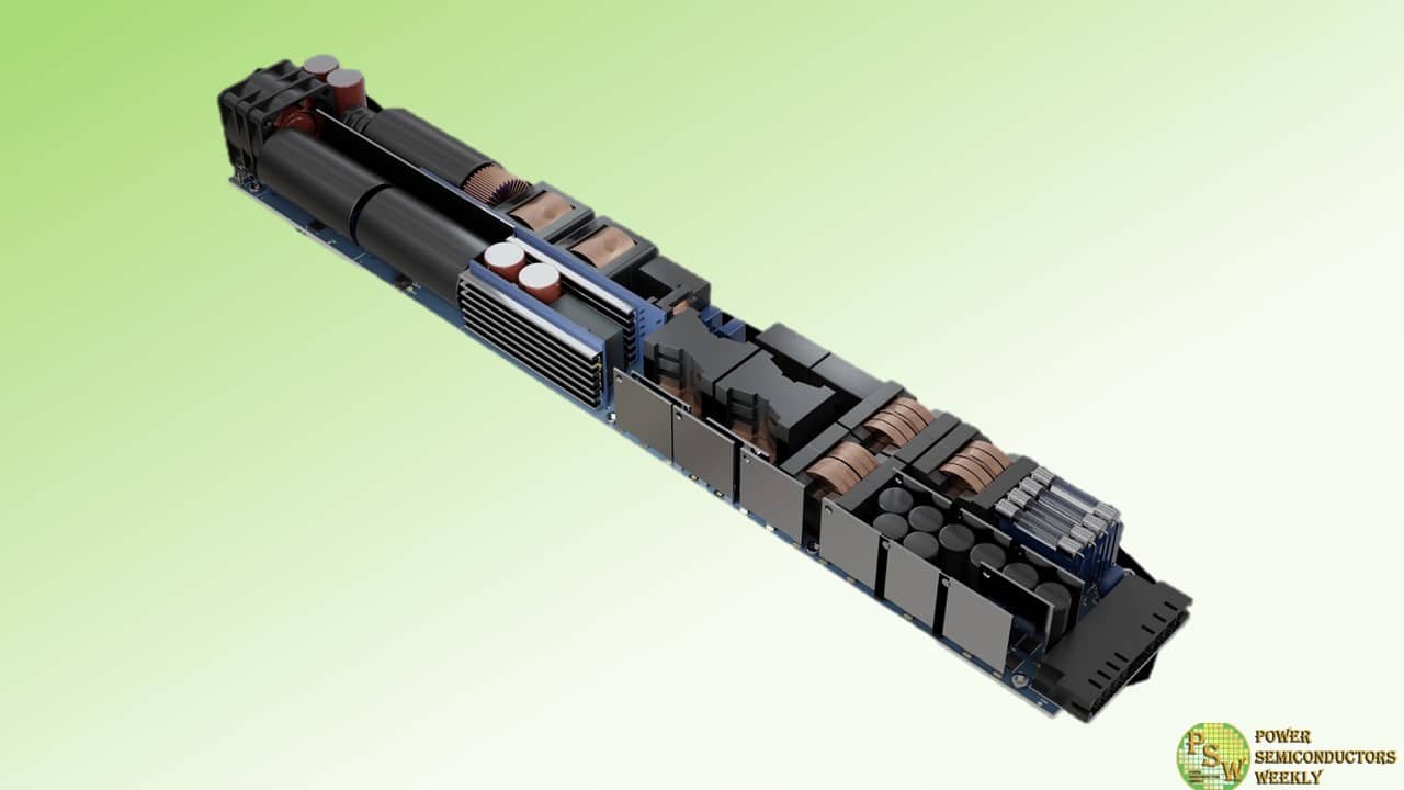
With the increasing power requirements of Artificial Intelligence (AI) processors, server power supplies (PSUs) must deliver more and more power without exceeding the defined dimensions of the server racks. This is driven by a surge in energy demand of high-level GPUs, which could consume 2 kW and more per chip by the end of the decade.
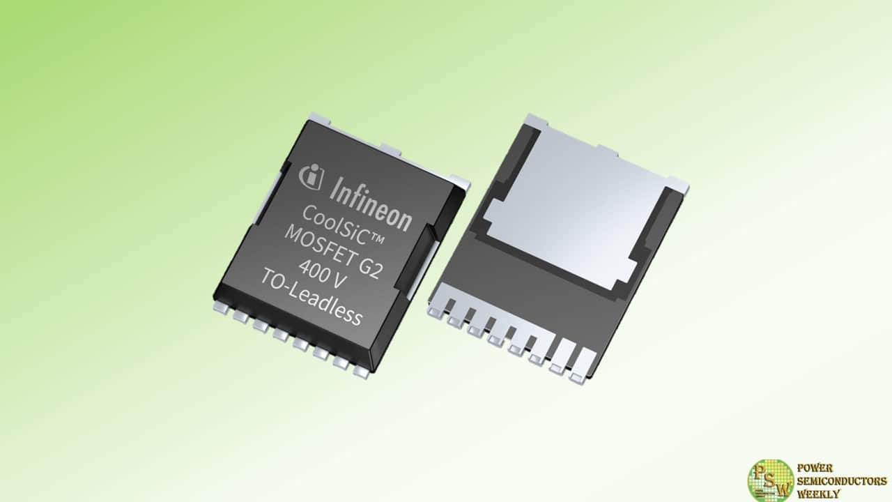
These needs, as well as the emergence of increasingly demanding applications and the associated specific customer requirements have prompted Infineon Technologies AG to extend the development of SiC MOSFETs to voltages below 650 V. The company is now launching the new CoolSiC™ MOSFET 400 V family, which is based on the second generation (G2) CoolSiC technology introduced earlier this year.
The new MOSFET portfolio was specially developed for use in the AC/DC stage of AI servers, complementing Infineon’s recently announced PSU roadmap. The devices are also ideal for solar and energy storage systems (ESS), inverter motor control, industrial and auxiliary power supplies (SMPS) as well as solid-state circuit breakers for residential buildings.
“Infineon offers an extensive portfolio of high-performance MOSFETs and GaN transistors to meet the demanding design and space requirements of AI server power supplies”, said Richard Kuncic, Head of the Power Systems Business Line at Infineon. “We are committed to supporting our customers with advanced products such as the CoolSiC MOSFETs 400 V G2 to drive highest energy efficiency in advanced AI applications.”
The new family features ultra-low conduction and switching losses when compared to existing 650 V SiC and Si MOSFETs. Implemented in a multi-level PFC, the AC/DC stage of the AI Server PSU can attain a power density of more than 100 W/in³ and is proven to reach 99.5 percent efficiency.
This is an efficiency improvement of 0.3 percentage points over solutions using 650 V SiC MOSFETs. In addition, the system solution for AI Server PSUs is completed by implementing CoolGaN™ transistors in the DC/DC stage. With this combination of high-performance MOSFETs and transistors, the power supply can deliver more than 8 kW with an increase in power density by a factor of more than 3 compared to current solutions.
The new MOSFET portfolio comprises a total of 10 products: five R DS(on) classes from 11 to 45 mΩ in Kelvin-source TOLL and D²PAK-7 packages with .XT package interconnect technology. The drain-source breakdown voltage of 400 V at T vj = 25°C. makes them ideal for use in 2- and 3-level converters and for synchronous rectification.
The components offer high robustness under harsh switching conditions and are 100 percent avalanche tested. The highly robust CoolSiC technology in combination with the .XT interconnect technology enables the devices to cope with power peaks and transients caused by sudden changes in the power requirements of the AI processor. Both the connection technology and a low and positive R DS(on) temperature coefficient enable excellent performance under operating conditions with higher junction temperatures.
Original – Infineon Technologies
-
The influence of artificial intelligence (AI) is driving up the energy demand of data centers across the globe. This growing demand underscores the need for efficient and reliable energy supply for servers. Infineon Technologies AG opens a new chapter in the energy supply domain for AI systems and unveils a roadmap of energy efficient power supply units (PSU) specifically designed to address the current and future energy need of AI data centers.
By introducing unprecedented PSU performance classes, Infineon enables cloud data center and AI server operators to reduce their energy consumption for system cooling. The innovative PSUs reduce power consumption and CO 2 emissions, resulting in lower lifetime operating costs. The powerful PSUs are not only used in future data centers but can also replace existing power supply units in servers and increase efficiency.
In addition to the current PSUs with an output of 3 kW and 3.3 kW available today, the new 8 kW and 12 kW PSUs will contribute to further increasing energy efficiency in future AI data centers. With the 12 kW reference board, Infineon will offer the world’s first power supply unit that achieves this level of performance and supplies future data centers with power.
“At Infineon, we power AI. We are addressing a critical question of our era – how to efficiently meet the escalating energy demands of data centers,” says Adam White, Division President Power & Sensor Systems at Infineon. “It’s a development that was only possible by Infineon’s expertise in integrating the three semiconductor materials silicon (Si), silicon carbide (SiC), and gallium nitride (GaN) into a single module. Our PSU portfolio is therefore not only an example of Infineon’s innovative strength, which leads to first-class results in terms of performance, efficiency and reliability for data centers and the AI ecosystem. It also reinforces Infineon’s market leadership in power semiconductors.”
Infineon is responding to the requirements of data center operators for higher system efficiency and lower downtimes. The growth of server and data center applications has led to an increase in power requirements, necessitating the development of power supplies with higher power ratings from 800 W up to 5.5 kW and beyond. This increase is driven by the growing power requirements of Graphic Process Units (GPU) on which AI applications are computed.
High-level GPUs now require up to 1 kW per chip reaching 2 kW and beyond by the end of the decade. This will lead to higher overall energy demand for data centers. Depending on the scenario, data centers will account for up to seven percent of global electricity consumption by 2030; this is an order of magnitude comparable to India’s current electricity consumption.
Infineon’s new PSUs contribute to the efforts to limit the CO 2 footprint of AI data centers despite the rapidly growing energy requirements. This is made possible by a particularly high level of efficiency that minimizes power losses. Infineon’s new generation PSUs achieve an efficiency of 97.5 percent and meet the most stringent performance requirements. The new 8 kW PSU is capable of supporting AI racks with an output of up to 300 kW and more. Efficiency and power density is increased to 100 watts per in³ compared to 32 W/in³ in the available 3 kW PSU, providing further benefits for the system size and cost savings for operators.
From a technical perspective, this is made possible by the unique combination of the three semiconductor materials Si, SiC and GaN. These technologies contribute to the sustainability and reliability of AI server and data center systems. Innovative semiconductors based on wide-bandgap materials such as SiC and GaN are the key to a conscious and efficient use of energy to drive decarbonization.
The 8 kW Power Supply Unit will be available in Q1 2025. For more information about the PSU roadmap, please click here.
Infineon at the PCIM Europe 2024
PCIM Europe will take place in Nuremberg, Germany, from 11 to 13 June 2024. Infineon will present its products and solutions for decarbonization and digitalization in hall 7, booths #470 and #169. Company representatives will also be giving several presentations at the accompanying PCIM Conference and Forums, followed by discussions with the speakers. Information about Infineon’s PCIM 2024 show highlights is available at www.infineon.com/pcim.
Original – Infineon Technologies
-

PANJIT introduced its latest 60, 100, and 150V AEC-Q101 qualified MOSFETs, engineered with advanced trench technology to set new standards in performance and efficiency. Designed for both automotive and industrial power systems, these MOSFETs offer unparalleled figure of merit (FOM), significantly lower RDS(ON), and reduced capacitance. This ensures minimal conduction and switching losses, resulting in enhanced overall electrical performance.
The new MOSFET series is available in various packages, including DFN3333-8L, DFN5060-8L, DFN5060B-8L, TO-252AA and TO-220AB-L. These compact packages facilitate efficient design solutions for modern electronic systems. With an operating junction temperature of up to 175°C, these MOSFETs are robust and reliable, further evidenced by their AEC-Q101 qualification.
These MOSFETs are ideal for various automotive applications, including wireless charging transmitters, battery management systems, front and rear lighting systems, DC/DC converters, infotainment systems and more. Their low on-resistance and high efficiency enhance the performance and reliability of these systems. Additionally, their versatility extends to industrial power systems, broadening their range of applicability and utility.
PANJIT’s new automotive-grade MOSFET series delivers superior performance, reliability, and efficiency. These MOSFETs are set to become a cornerstone in the design of next-generation automotive and industrial systems.
Original – PANJIT International
-
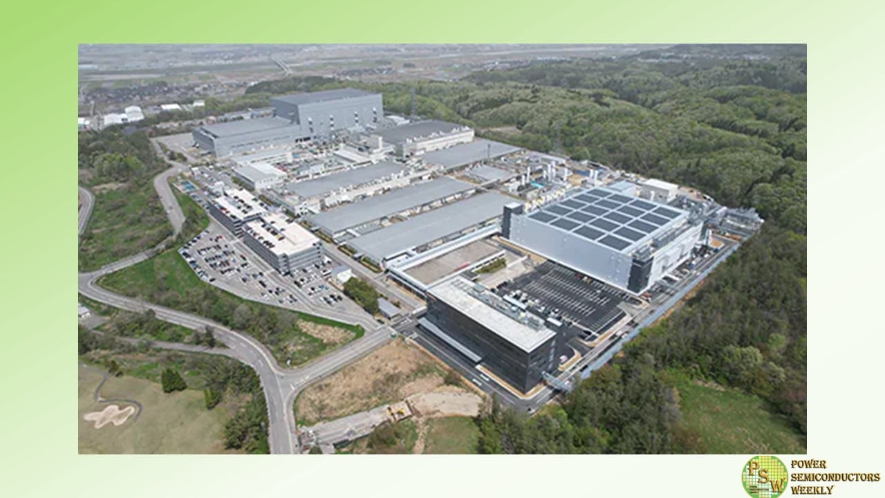
Toshiba Electronic Devices & Storage Corporation held a ceremony to mark the completion of a new 300-millimeter wafer fabrication facility for power semiconductors and an office building at Kaga Toshiba Electronics Corporation in Ishikawa Prefecture, Japan, one of Toshiba’s key group companies. The completion of construction is a major milestone for Phase 1 of Toshiba’s multi-year investment program.
Toshiba will now proceed with equipment installation, toward starting mass production in the second half of fiscal year 2024. Once Phase 1 reaches full-scale operation, Toshiba’s production capacity for power semiconductors, mainly MOSFETs and IGBTs, will be 2.5 times that of fiscal 2021, when the investment plan was made. Decisions on the construction and start of operation of Phase 2 will reflect market trends.
The new manufacturing building follows and will make a major contribution to Toshiba’s Business Continuity Plan (BCP): it has a seismic isolation structure that absorbs earthquake shock and redundant power sources. Energy from renewable source and solar panels on the roof of the building (onsite PPA model) will allow the facility to meet 100% of its power requirement with renewable energy.
Product quality and production efficiency will be boosted by the use of artificial intelligence (AI). Toshiba expects to receive a grant from the Ministry of Economy, Trade and Industry of Japan to subsidize its investment in part of the manufacturing equipment.Power semiconductors play a crucial role in electricity supply and control, and are essential devices for energy efficiency in all electrical equipment. With the continuing electrification of automobiles and the automation of industrial machinery, they are expected to see continued robust demand growth. Toshiba started power semiconductor production on a new 300-millimeter wafer line in the second half of fiscal 2022 at Kaga Toshiba Electronics’ existing facility. Going forward, the company will expand production with the new fab and further contribute to carbon neutrality.
Overview of Kaga Toshiba Electronics Corporation
Location: 1-1, Iwauchi-machi, Nomi-shi, Ishikawa Prefecture, Japan
Established: December, 1984
President and Representative Director: Satoshi Aida
Employees: 1,150 (as of March 31, 2024)
Main Products: Discrete semiconductors (power semiconductors, small-signal devices and optoelectronic devices)
Web: Kaga Toshiba Electronics CorporationOriginal – Toshiba
-

Analog Devices, Inc. announced financial results for its fiscal second quarter 2024, which ended May 4, 2024.
“ADI delivered second quarter revenue above the midpoint of our outlook, despite continued macro and inventory headwinds. Further, the strength and resiliency of our business model, coupled with disciplined cost control, enabled us to achieve profitability and earnings per share above the high-end of our outlook,” said Vincent Roche, CEO and Chair.
“We believe inventory rationalization across our broad customer base is stabilizing, clearing a path for us to return to sequential growth in the third quarter. This, coupled with improving new orders, gives us optimism that we are at the beginning of a cyclical recovery.”
Roche continued, “The continued proliferation of the Intelligent Edge presents ADI with numerous concurrent secular growth vectors. AI, where we have been increasing our investments, is expected to accelerate these trends as it increasingly extends from centralized applications in data centers to a myriad of applications at the physical edge. As a leader of real-world data creation, processing, and connectivity, our solutions are becoming increasingly important to customers in the AI-driven era. As such, my confidence in ADI’s ability to drive long term value for all stakeholders remains resolute.”
For the third quarter of fiscal 2024, company’s forecas revenue is $2.27 billion, +/- $100 million. At the midpoint of this revenue outlook, reported operating margin is expected on the level of approximately 20.1%, +/-200 bps, and adjusted operating margin of approximately 40.0%, +/-100 bps. Analog Devices is planning for reported EPS to be $0.71, +/-$0.10, and adjusted EPS to be $1.50, +/-$0.10.
The company’s third quarter fiscal 2024 outlook is based on current expectations and actual results may differ materially as a result of, among other things, the important factors discussed at the end of this release. These statements supersede all prior statements regarding business outlook set forth in prior ADI news releases, and ADI disclaims any obligation to update these forward-looking statements.
Performance for the Second Quarter 2024 Financials
Original – Analog Devices
