-
Soitec and Tokai Carbon, a comprehensive manufacturer of carbon and graphite products, have entered into a strategic partnership for the development and supply of polycrystalline silicon carbide substrates specifically designed for Soitec SmartSiC™ wafers.
Silicon carbide is a disruptive compound semiconductor and SmartSiC™ engineered substrates accelerate the adoption of silicon carbide for electric mobility, industrial and smart grid applications by delivering superior manufacturing and cost efficiencies with an improved environmental footprint.
Under this partnership, which will see Tokai Carbon supply 150mm and 200mm poly-SiC wafers to Soitec, the two companies are harnessing their advanced R&D capabilities to enhance the SmartSiC™ ecosystem. Tokai Carbon’s advanced technology and manufacturing capacity in polycrystalline silicon carbide (polySiC) combined with the right to use Soitec specifications for polySiC coarse wafers compliant with Soitec SmartSiC™ is expected to make a strategic contribution to the global ramp-up of SmartSiC™ wafer production.
Cyril Menon, Chief Operations Officer of Soitec, stated: “This partnership with Tokai marks yet another key step in the ramp-up of Soitec’s SmartSiC™ technology to address fast-growing markets such as electric mobility and industrial electrification. Tokai’s top quality SiC products and R&D capabilities, combined with Soitec’s innovative SmartSiC™ technology, can help to accelerate global adoption of electric mobility and other SiC technologies. This is an important milestone in terms of perception and value creation for the SmartSiC™ ecosystem.”
Hajime Nagasaka, CEO of Tokai Carbon, commented. “The polycrystalline SiC substrate to be supplied to Soitec is a strategic product in our solid SiC product series. We are pleased to see our long years of research and development come to fruition in this way, and we have high expectations for this product in the SiC semiconductor market, which is expected to expand significantly in the future. The partnership with Soitec is also very meaningful in terms of contributing to the realization of a sustainable society.”
Original – Soitec
-
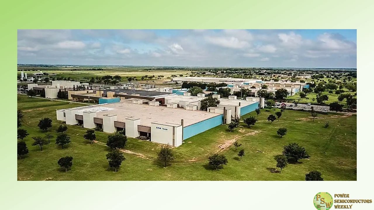
X-FAB and Soitec will begin work to offer Soitec’s SmartSiC™ wafers for the production of silicon carbide power devices at X-FAB’s plant in Lubbock, Texas.
This collaboration follows the successful completion of the assessment phase, during which silicon carbide (SiC) power devices were manufactured at X-FAB Texas on 150mm SmartSiC™ wafers. Soitec will offer X-FAB’s customers easy access to the SmartSiC™ substrate through a joint supply chain consignment model.
X-FAB is the pioneer and leader of the foundry model in the fast-growing SiC market. Silicon carbide (SiC) is a disruptive compound semiconductor material with intrinsic properties providing superior performance and efficiency over silicon in power applications.
SmartSiC™ is a proprietary Soitec technology based on the company’s SmartCut™ process, in which a thin layer of a high-quality monocrystalline (mono-SiC) ‘donor’ wafer is split off and bonded to a low resistivity polycrystalline (poly-SiC) ‘handle’ wafer. The resulting substrate offers improved device performance and manufacturing yields. The process allows multiple re-uses of a single donor wafer, significantly reducing cost and related CO2 emissions.In this fast-growing market, Soitec is ramping production of SmartSiC™ substrates at its new plant of Bernin, near Grenoble (France). X-FAB is increasing production capacity for SiC devices at the Lubbock plant. The use of the SmartSiC™ substrate enables X-FAB’s customers to design smaller devices, resulting in efficiency improvements through an increased number of dies per wafer. The benefit of reduced CO2 emissions from the substrate manufacturing process will also contribute to X-FAB’s initiative to reduce its overall carbon footprint.
Sophie Le-Guyadec VP Procurement of X-FAB, states: “As the leading SiC foundry, we want to provide our customers the full range of opportunities to design innovative and robust SiC devices for electric vehicles, renewable power and industrial applications. To offer the most advanced silicon carbide processes and manufacturing capabilities, we jointly agreed to provide our customers easy access to Soitec’s innovative SmartSiC™ via a consignment model.”
Emmanuel Sabonnadiere, Soitec Executive Vice President Automotive and Industry comments: “Soitec’s SmartSiC substrates and X-FAB’s foundry services are a perfect fit to meet increasing demand for new SiC products. This cooperation is a significant milestone for the deployment of SmartSiC in the U.S. market and internationally, thanks to X-FAB’s global footprint.”Original – X-FAB
-

Toshiba Electronic Devices & Storage Corporation announced new board of directors, with an effective date of June 1, 2024. The composition of the Board of Directors and the company’s Auditors, as of June 1, 2024, will be as follows:
Directors and Officers of the Company:
- Director, President & CEO – Taro SHIMADA (Toshiba Corporation)
- Director, Vice President – Noriyasu KURIHARA
- Director – Seiichi MORI
- Director – Shin KUROSAWA
- Director – Hiroyuki SHINKI (Toshiba Corporation)
- Director – Masazumi TOMISHIGE (Toshiba Corporation)
- Director – Takanori NAKAZAWA (Toshiba Corporation)
- Director – Yutaka SATA (Toshiba Corporation)
- Auditor – Hiroki OKADA
- Auditor – Masami TAKAOKA
- Auditor – Akira NAKANISHI (Toshiba Corporation)
Retiring Directors as of June 1, 2023:
- Norifumi INUKUBO
- Hiroshi KURIKI
Original – Toshiba
-
Soitec announced its revenue for the fourth quarter of fiscal year 2024 and its full-year results of fiscal year 2024 (ended on March 31st, 2024). The financial statements were approved by the Board of Directors during its meeting.
- Q4’24 revenue reached €337m, down 2% at constant exchange rates and perimeter compared to the record quarter Q4’23
- FY’24 revenue amounted to €978m, down 10% both at constant exchange rates and perimeter and on a reported basis, in line with latest guidance
- FY’24 EBITDA margin at the level of 34%, also in line with latest guidance
- FY’24 net profit, reached €178m, an 18% margin
- FY’25 outlook confirmed: Soitec expects revenue to be stable year-on-year at constant exchange rates and perimeter and EBITDA margin to reach around 35%
- Changes in the Board of Directors: Frédéric Lissalde to be proposed as Director at the next Annual General Meeting
Pierre Barnabé, Soitec’s CEO, commented: “Fiscal year 2024 was a challenging year, marked by the impact on our sales of RF-SOI inventories correction across the entire smartphone value chain. Despite these difficult market conditions, we succeeded in maintaining a solid level of profitability, while continuing to invest both in innovation and industrial capacity to prepare for the future.
Regarding our fiscal year 2025, the RF-SOI inventory correction will continue to impact our revenue through the first part of the year. However, we are seeing early signs of improvement downstream, led by the ongoing return to growth of the smartphone market, which gives us confidence in the recovery of our RF-SOI sales in the second half of the year. At the same time, we will continue to benefit from strong performance of our other SOI products, and from the successful expansion of our product portfolio, with increased penetration of POI and the ramp-up of SmartSiC.
Looking ahead, we remain very confident in our ability to leverage the significant growth drivers underpinning our three end-markets. Coupled with the increasing adoption of engineered substrates to deliver more powerful and energy-efficient solutions to a growing number of customers, our continued diversification and expansion of our product portfolio, in both SOI and Compound substrates, supports our clear vision towards $2bn revenue in the medium term, with significant margin expansion potential,” added Pierre Barnabé.
Original – Soitec
-
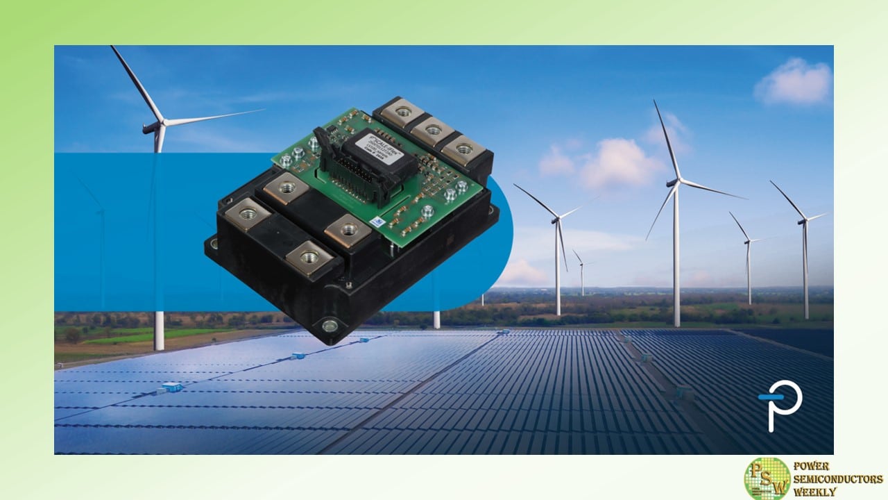
Power Integrations announced the launch of the SCALE-iFlex™ XLT family of dual-channel plug-and-play gate drivers for operation of single LV100 (Mitsubishi), XHP™ 2 (Infineon), HPnC (Fuji Electric) and equivalent semiconductor modules up to 2300 V blocking voltage for wind, energy storage and solar renewable energy installations.
This single-board driver enables active thermal management of inverter modules for improved system utilization and reduces the bill-of-material count for increased reliability.
Thorsten Schmidt, product marketing manager at Power Integrations commented: “It’s a real challenge to build a single-board gate driver for these ‘new dual’ style IGBT modules. Our compact new SCALE-iFlex XLT gate drivers fit inside the outline of the module, allowing the drivers to be mounted on the module, which gives converter system designers a high degree of mechanical design freedom.”
SCALE-iFlex XLT dual-channel gate drivers feature Negative Temperature Coefficient (NTC) data reporting – an isolated temperature measurement of the power module – which allows accurate thermal management of converter systems. This enables system designers to optimize thermal design and obtain a 25 to 30 percent converter power increase from the same hardware.
The isolated NTC readout also reduces hardware complexity, eliminating multiple cables, connectors and additional isolation barrier crossing circuits. The new gate drivers employ Power Integrations’ SCALE-2 chip set which minimizes component count, enhancing reliability. The gate driver board also protects the power switches in the event of a short-circuit.
Original – Power Integrations
-

GlobalFoundries announced a partnership with Micron Technology, Inc. and the U.S. National Science Foundation (NSF) to invest in workforce development at Minority Serving Institutions (MSI) to help meet the growing workforce needs of the U.S. semiconductor ecosystem.
In partnership with Micron and the NSF, the investment will support semiconductor workforce development at Historically Black College and Universities, Hispanic Serving Institutions, Asian American Native American Pacific Islander-Serving Institutions and Tribal Colleges and Universities throughout the U.S. These investments aim to diversify the semiconductor workforce and build robust talent pathways through education and career reentry initiatives.
The companies’ and NSF ’s support of U.S. MSIs is directly aligned with the workforce development objectives of the federal CHIPS and Science Act as well as New York State’s Green Chips legislation, to ensure a robust pipeline of U.S. semiconductor talent.
“As an industry, we must work together to collectively address the great need for a robust, diverse pipeline of talented individuals who will be the semiconductor innovators and leaders of tomorrow,” said Pradheepa Raman, chief people officer of GF. “Strong public-private partnerships, like our collaboration with Micron and NSF to support Minority Serving Institutions, are critical to continue the work of inspiring and developing the skilled workforce our industry needs to grow.”
“Partnering with leaders in industry, government and education to meet the needs of a growing semiconductor workforce in the U.S. is an essential part of nurturing the talent necessary to fill key openings in the semiconductor industry,” said Erwin Gianchandani, NSF assistant director for Technology, Innovation and Partnerships. “We look forward to collaborating with our partners to increase access to equitable education, address student programming and teacher and faculty professional development and strengthen infrastructure through future funding opportunities.”
“Micron’s investments in U.S. expansion are about much more than building fabs. We’re investing in people and in partnerships to expose learners from every background to opportunities they may not otherwise have without support,” said April Arnzen, executive vice president and chief people officer at Micron and president of the Micron Foundation. “We’re honored to see initiatives like Micron’s MSI Semiconductor Network, which are at the forefront of our industry’s efforts to prepare the semiconductor workforce and research ecosystem to meet growing demand for talent, recognized by government leaders in the U.S. and globally.”
“Micron’s and GlobalFoundries’ historic investments are transformative for Upstate New York and the nation, and today’s announcement will put in place another critical workforce development initiative to deliver the workers needed to fill the tens of thousands of new jobs that will be created. This initiative will especially focus on connecting underserved and historically marginalized New Yorkers and others around the country to new job opportunities in the semiconductor industry, including to build chips in Upstate NY,” said Senate Majority Leader Chuck Schumer.
“In recent weeks, my CHIPS & Science Law delivered a whopping $6.1 billion for Micron to build their mega-fab project and another $1.5 billion for GlobalFoundries’ expansion. Now, Micron and GlobalFoundries are working to develop a workforce pipeline to train and attract the next generation of talent, putting students from our top-notch educational institutions into jobs in the semiconductor industry. I am glad this initiative is supported by National Science Foundation funds from my CHIPS & Science Law, which serves as the fuel for major investments like Micron’s and GlobalFoundries’ to bring chip manufacturing back to America and helping our future scientists and engineers reach new heights with good-paying jobs right at their doorstep.”
“We are excited about the opportunities to grow efforts with GlobalFoundries that have led to increased summer internships and experiences at GF’s Malta, NY, facility for students at multiple CUNY schools including LaGuardia, Queensborough and City Tech,” said Tavis Ezell, director of business development for The City University of New York’s (CUNY) Advanced Science Research Center (ASRC). “With our industry partners, we are identifying the necessary skills needed to support jobs across the vast semiconductor ecosystem and bolster current curricula across a wide range of CUNY degrees, connecting interested students to training opportunities, whether their first internship experience is at the ASRC, or at an industry partner such as GlobalFoundries.”
GF’s support of MSIs is the company’s latest effort to build a critical talent pipeline for a current and future workforce. In November 2023, the company announced a new student loan repayment program to help U.S.-based employees and eligible new recruits pay up to $28,500 in student loan debt, tax-free, to help ease the financial burden of higher education and training. GF also offers tuition reimbursement for employees pursuing undergraduate and graduate degrees, fully paid parental leave, employee fitness stipend to promote good health and childcare subsidy towards dependent care. GF’s first-of-its-kind apprenticeship program provides opportunities for individuals with no prior experience or training in the semiconductor industry, offering full-time paid positions and cost-free college courses to high school graduates.
GF has established strategic partnerships nationwide with top universities and strong regional engagements with community colleges in New York and Vermont as well as access to worldwide talent through its global footprint to help build a diverse workforce and semiconductor talent pipeline. To help inspire younger children, GF has a robust STEM outreach program to engage with regional middle schools and high schools, including Early College High School and Career and Technical Education programs, to bring industry awareness and hands-on experiences to students.
Original – GlobalFoundries
-

Navitas Semiconductor invites visitors to experience “Planet Navitas” at PCIM 2024 (June 11th-13th) and see how industry-leading GaN and SiC solutions deliver optimal performance in a broad array of fast-growing markets and applications from 20 W to 20 MW.
Aligned with Navitas’ mission to “Electrify Our World™”, the “Planet Navitas” booth invites visitors to discover how next-gen GaN and SiC technology enable the latest solutions for fully-electrified EV transportation, AI data centers, industrial compressors, drives, and robotics plus renewable energy sourcing and storage.
Each example highlights end-user benefits such as increased portability, longer range, faster charging, and grid independence, along with a focus on how low-carbon-footprint GaN and SiC technology can save over 6 Gtons/yr CO2 by 2050.
“PCIM is a key event in the power-electronics calendar,” says Alessandro Squeri, Navitas’ senior director for European sales. “Complementary GaNFast and GeneSiC portfolios, with comprehensive, application-specific system design support, accelerate customer time-to-market with sustainable performance advantages. ‘Planet Navitas’ represents the very real, inspiring implementation of GaN & SiC that makes up a $1.6B identified customer pipeline as part of a vast $22B/year market opportunity.”
Major technology updates and releases include GaNSafe™ – the world’s most-protected, most reliable, and highest-performance GaN power, Gen-4 GaNSense™ Half-Bridge ICs – the most integrated GaN devices, and Gen-3 Fast GeneSiC power FETs – for game-changing motor drive and energy-storage applications.
In addition to the exhibition, PCIM 2024 includes peer-review technical presentations, including:
11th June, 13:00 – 14:30, Hall 10.1
- “Low-Cost High-Density 300 W / 20 V AC-DC Converter Enabled by GaN Power ICs”– Tom Ribarich, Sr. Director of Strategic Marketing, Navitas Semiconductor
- A low-cost 300 W high-density AC-to-DC converter has been designed and demonstrated to achieve >96% peak efficiency and 270 cc. The circuit topologies include a 2-phase interleaved PFC input stage, an LLC DC-DC stage, and a synchronous rectification output stage. The design includes GaN Power ICs and off-the-shelf controllers running at 300 kHz. This new design has resulted in a cased power density of 1.1 W/cc.
12th June, 15:30 – 17:00, Foyer
- Evaluation of SiC Devices for Over 500 kHz Application Based on Buck Circuit – Minli Jia, Sr. Staff Applications Engineer, Navitas Semiconductor
- This paper selects three 1200 V SiC devices of similar specifications and different manufacturers for analysis and experimental research and designs a Buck converter with an output power of 3.6 kW and a switching frequency of 600 kHz. The efficiency and heat of three SiC types were tested under the same working conditions, and the results showed that the SiC with fast turn-off characteristics and low thermal resistance was more suitable for high-frequency converter applications.
Original – Navitas Semiconductor
- “Low-Cost High-Density 300 W / 20 V AC-DC Converter Enabled by GaN Power ICs”– Tom Ribarich, Sr. Director of Strategic Marketing, Navitas Semiconductor
-

Nexperia announced that it is now offering its industry leading 1200 V silicon carbide (SiC) MOSFETs in D2PAK-7 surface mount device (SMD) packaging, with a choice of 30, 40, 60, and 80 mΩ RDSon values. This announcement follows on from Nexperia’s late-2023 release of two discrete SiC MOSFETs in 3 and 4-pin TO-247 packaging and is the latest offering in a series which will see its SiC MOSFET portfolio swiftly expand to include devices with RDSon values of 17, 30, 40, 60 and 80 mΩ in flexible package options.
With the release of the NSF0xx120D7A0, Nexperia is addressing the growing market demand for high performance SiC switches in SMD packages like D2PAK-7, which is becoming increasingly popular in various industrial applications including electric vehicle (EV) charging (charge pile, offboard charging), uninterruptible power supplies (UPS) and inverters for solar and energy storage systems (ESS).
It is also further testimony to Nexperia’s successful strategic partnership with Mitsubishi Electric Corporation (MELCO), which has seen the two companies join forces to push the energy efficiency and electrical performance of SiC wide bandgap semiconductors to the next level, while additionally future-proofing production capacity for this technology in response to ever growing market demand.
RDSon is a critical performance parameter for SiC MOSFETs because it impacts conduction power losses. However, many manufacturers concentrate on the nominal value, neglecting the fact that it can increase by more than 100% as device operating temperatures rise, resulting in considerable conduction losses.
Nexperia identified this as a limiting factor in the performance of many currently available SiC devices and leveraged the features of its innovative process technology to ensure that its new SiC MOSFETs offer industry-leading temperature stability, with the nominal value of RDSon increasing by only 38% over an operating temperature range from 25 °C to 175 °C.
Tightest threshold voltage, VGS(th) specification, allows these discrete MOSFETs to offer balanced current-carrying performance when connected in parallel. Furthermore, low body diode forward voltage (VSD) is a parameter which increases device robustness and efficiency, while also relaxing the dead-time requirement during freewheeling operation.
Original – Nexperia
-

GlobalFoundries announced the appointment of industry and company veteran, Kay Chai (KC) Ang, as president of Asia and Chairman of China. With over 30 years of semiconductor foundry experience, Mr. Ang will lead new business development and strategic partnerships across Asia with a focus on China.
Mr. Ang joined GF in 2010 and has served in a variety of senior leadership roles for the company including most recently as Chief Manufacturing Officer with responsibility for GF’s global sites as well as previously as head of all GF’s Singapore operations.
Prior to joining GF, Mr. Ang held senior leadership positions at Chartered Semiconductor Manufacturing, including Senior Vice President of Sales and Marketing with responsibility for global sales, marketing, services, customer support and regional business operations.
Mr. Ang has been a key player in the growth of Singapore’s chip industry. He serves on the Board of the National Research Foundation in Singapore and is the Chairman of the SEMI Southeast Asia Regional Advisory Board.
“At GF, we leverage our global footprint to provide our customers with the secure, essential chips they need, where they want them produced,” said Niels Anderskouv, chief business officer at GF. “Given his more than 30 years experience coupled with his long-standing relationships with some of Asia’s most senior semiconductor industry leaders, KC is the ideal leader to drive customer engagements and partnerships across Asia and accelerate GF’s business growth within the China market in particular.”
“I am excited about this next stage of my career. I am looking forward to partnering with my commercial, technical and product management colleagues to expand GF’s relationships and be a trusted, dependable partner for our customers,” said KC Ang, president, Asia & Chairman, China at GF.
“The differentiated technology solutions that we offer combined with our manufacturing excellence, especially in key end markets such as automotive, make us a perfect partner for fast growing customers in Asia. In addition, we are responding to many of our existing multi-national customers who are looking for ways to partner with GF to serve the growing demands of their Chinese end customers with high quality manufacturing and essential chip technologies.”
Original – GlobalFoundries
-

Transphorm, Inc. announced that its PCIM 2024 showcase will underscore its ability to outperform competitive wide bandgap technologies in higher power systems. For example, Transphorm’s normally-off d-mode SuperGaN®platform delivers higher electron mobility resulting in lower crossover losses versus Silicon Carbide—making it more a cost-effective, higher performing solution for various electric vehicle, datacenter/AI, infrastructure, renewable energy, and other broad industrial applications. To learn more, visit Transphorm during PCIM in Hall 7, Stall 108 during June 11 to 13, 2024.
Transphorm SuperGaN FETs are in production in a wide range of customer products crossing the power spectrum from low 45 W power adapters to higher power 7.5 kW PSUs. Many of these customer products are the first publicly recognized GaN-based systems of their kind and uniquely demonstrate advantages enabled only by the SuperGaN platform.
Examples include the previously mentioned liquid-cooled 7.5 kW PSU for mission-critical datacenter/blockchain applications; a 2.7 kW server CRPS with > 82 W/in3 power density (highest in any GaN power system available today); and 2.2 kW and 3 kW rack-mount 1U uninterruptible power supplies (UPSes). These design wins illustrate Transphorm’s ability to drive GaN into the various application markets composing an estimated GaN TAM of $8 billion by 2028.
In addition to real-world customer products, Transphorm continues to lead in technological achievements having recently demonstrated a 5 microsecond short-circuit withstand time, a bidirectional four-quadrant switch, and a 1200 V GaN-on-Sapphire device.
On-site demonstrations will include Transphorm solutions for 2- and 3-wheeler electric vehicle chargers along with customer PSUs for renewable energy systems, data centers, and more.
Speaking Engagement
Learn more about how Transphorm’s GaN solutions outperform competitive technologies and enable cross-industry innovations during the Bodo’s Power Systems session.
Panel: GaN Wide Bandgap Design, the Future of Power
Speaker: Philip Zuk, Senior Vice President, Business Development and Marketing
Date: June 12
Time: 2:20 – 3:20 p.m. CEST
Location: Hall 7, Stall 743Original – Transphorm
