-

Magnachip Semiconductor Corporation announced financial results for the first quarter 2024.
YJ Kim, Magnachip’s Chief Executive Officer, commented, “In Q1 we started the initial revenue ramp for OLED DDICs for the after-service market, and we were awarded two new designs targeted for a leading China smartphone OEM and also for a leading European EV maker. Our Power Analog Solutions (PAS) business revenue grew 12% sequentially driven by smartphones, e-motors, consumer appliances and server power applications, and we now are launching a slate of next-gen power products to help sustain our momentum. We also are encouraged that the power channel inventory showed signs of improvement in the first quarter.”
YJ continued, “Looking forward, we expect sequential revenue growth in Mixed-Signal Solutions (MSS) and PAS to continue in Q2 and we reiterate our prior full-year guidance for double digit growth in both MSS and PAS businesses.”
Financial Highlights
- Q1 consolidated revenue was $49.1 million, within our guidance range of $46-51 million.
- Q1 standard product business revenue was up 10.6% sequentially.
- Q1 consolidated gross profit margin was 18.3%, within our guidance range of 17-20%.
- Q1 standard product business gross profit margin was down 170 basis points sequentially, mostly due to lower Gumi fab utilization driven by the wind-down of Transitional Foundry Services.
- Ended Q1 with $29.7 million in long-term borrowing and $171.6 million in cash.
- Repurchased approximately $4.1 million or 0.6 million shares during the quarter.
Operational Highlights
- Secured a new high-end smartphone OLED DDIC design for a top tier China smartphone OEM.
- Secured a new EV automotive OLED DDIC design win for a leading European automaker.
- Began operations of our new China entity called Magnachip Technology Company (MTC). Our China headquarters is now up and running.
- Started initial ramp in Q1 for our first-generation OLED DDIC chip for China for the after-service market.
- Captured our first medium voltage MOSFET automotive design-win for an electric cooling fan with a China-based SUV supplier, as well as an additional automotive power steering related win in Korea.
- Began to see initial signs of inventory reductions in the distribution channel for our Power Analog Solutions products.
Original – Magnachip Semiconductor
- Q1 consolidated revenue was $49.1 million, within our guidance range of $46-51 million.
-
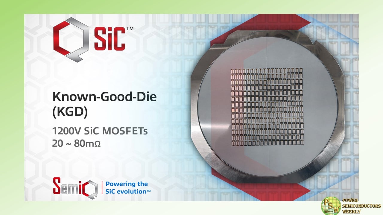
SemiQ has begun a known-good-die (KGD) screening program that delivers high-quality, electrically sorted and optically inspected advanced SiC MOSFET technology ready for back-end processing and direct die attachment.
Known-good-die from SemiQ ensures consistent electrical parameters, enabling customers to rely on repeatable performance for high end-of-line yield when building equipment such as high-voltage supplies, traction inverters, and power conditioning systems. Uniform die parameters also simplify the connection of multiple devices in high-power modules.
“SiC is a powerful technology aiding the global drive for sustainability and our known-good-die SiC MOSFETs from SemiQ provide important performance advantages, such as near-constant junction capacitance, low insertion loss, and high isolation needed for high-frequency applications,” says Michael Tsang, VP, Product Engineering and Operations at SemiQ. “Thanks to this program, customers can receive quality-assured dies that will streamline and improve productivity and deliver predictable and repeatable performance in high-efficiency applications.”
The KGD program is active now and applies to the complete portfolio of SemiQ’s QSiC™ 1200V SiC MOSFETs, ranging from 20mΩ to 80mΩ. This portfolio supports robust and efficient electrification across automotive, eMobility, renewable energy, industrial power, and other applications.
KGD devices are supplied post-singulation on a choice of carrier media including blue tape, pre-cured UV tape, and tape and reel to ease integration with customers’ processes. For more information, please visit SemiQ’s KGD page.
Original – SemiQ
-

Wolfspeed, Inc. announced its results for the third quarter of fiscal 2024.
Quarterly Financial Highlights (Continuing operations only. All comparisons are to the third quarter of fiscal 2023):
- Consolidated revenue of approximately $201 million, compared to approximately $193 million
◦ Mohawk Valley Fab contributed approximately $28 million in revenue, over a 2x increase from the prior quarter
◦ Materials revenue of approximately $99 million – second highest quarter on record - Power device design-ins of $2.8 billion
- Quarterly design-wins of $0.9 billion – 70% related to EV applications
- GAAP gross margin of 11%, compared to 31%
- Non-GAAP gross margin of 15%, compared to 34%
◦ GAAP and non-GAAP gross margins for the third quarter of fiscal 2024 include the impact of $30 million of underutilization costs, representing approximately 1,500 basis points of gross margin. See “Start-up and Underutilization Costs” below for additional information.
“We are pleased with the significant operational milestones achieved in the quarter for Wolfspeed as we continue to be the world’s first fully, vertically integrated 200-millimeter silicon carbide player at scale,” said Wolfspeed CEO, Gregg Lowe.
“We are making progress on our Mohawk Valley ramp, more than doubling revenue sequentially in the quarter and reaching more than 16% wafer start utilization in April, giving us confidence in our ability to achieve our 20% utilization target in June 2024. Construction continues at the JP, our 200mm materials factory in North Carolina. During the quarter, we started installing furnaces and connected the facility to the power grid, and we recently hosted our topping out ceremony. As we’ve said before, Mohawk Valley will be the flywheel of growth for Wolfspeed, and the JP will be instrumental in supplying it with high-quality materials. We are encouraged by the operational progress these facilities have made and how it will support our long-term growth trajectory.”
Lowe continued, “While there have been headlines around general demand weakness in EVs, we still have more demand than we can supply for the foreseeable future. Our second highest quarter of design-ins to date and more than $5 billion of designwins so far this fiscal year, tell a compelling story. While the industrial and energy end markets pose short-term headwinds to our results, we firmly believe in the strength of our long-term prospects as the electrification of all things continues across a broad set of applications.”
Original – Wolfspeed
- Consolidated revenue of approximately $201 million, compared to approximately $193 million
-

Qorvo® announced financial results for the Company’s fiscal 2024 fourth quarter ended March 30, 2024.
Strategic Highlights
- Grew quarterly revenue 49% year-over-year and exceeded the mid-point of revenue guidance by $16 million
- Completed acquisition of Anokiwave, a leading supplier of high-performance silicon integrated circuits for intelligent active array antennas for Defense, SATCOM, 5G, and other beam forming applications
On a GAAP basis, revenue for Qorvo’s fiscal 2024 fourth quarter was $941 million, gross margin was 40.6%, operating income was $30 million, and diluted earnings per share was $0.03. On a non-GAAP basis, gross margin was 42.5%, operating income was $147 million, and diluted earnings per share was $1.39.
Bob Bruggeworth, president and chief executive officer of Qorvo, said, “Qorvo delivered year-over-year revenue growth in the March quarter in each of our three operating segments. There are global macro trends supporting our markets that are increasing customer requirements for efficiency, latency, throughput, and other critical performance metrics where Qorvo delivers significant competitive advantage.
“During the quarter, we acquired Anokiwave, and we are excited to accelerate the adoption of their technology while developing more highly integrated system solutions that leverage our D&A and power management portfolios. Qorvo continues to expand our technology portfolio to drive growth and diversify our business across markets, customers and product categories.”
Financial Commentary and Outlook
Grant Brown, chief financial officer of Qorvo, said, “In fiscal 2024, Qorvo achieved significant content gains with key mobile customers and robust revenue growth in our defense and aerospace business. As we begin fiscal 2025, flagship smartphone ramps and large defense programs are down seasonally, and we expect product mix to trend toward mass market 5G products and associated higher-cost inventories in the June quarter. In the September quarter, we anticipate substantial sequential gross margin improvement. For full-year fiscal 2025, we expect modest revenue growth and margin improvement compared to fiscal 2024. We continue to take proactive steps to reduce capital intensity and structurally enhance our gross margin profile.”
Qorvo’s current outlook for the June 2024 quarter is:
- Quarterly revenue of approximately $850 million, plus or minus $25 million
- Non-GAAP gross margin between 40% and 41%
- Non-GAAP diluted earnings per share between $0.60 and $0.80
Original – Qorvo
-

Axcelis Technologies, Inc. announced financial results for the first quarter ended March 31, 2024.
The Company reported first quarter revenue of $252.4 million, compared to $310.3 million for the fourth quarter of 2023. Gross margin for the quarter was 46%, compared to 44.4% in the fourth quarter. Operating profit for the quarter was $56.5 million, compared to $79.1 million for the fourth quarter. Net income for the quarter was $51.6 million, or $1.57 per diluted share, compared to $71.1 million, or $2.15 per diluted share in the fourth quarter.
President and CEO Russell Low commented, “Axcelis is off to a good start in 2024. The Company delivered strong financial results in the first quarter, as a result of continued execution by the Axcelis team combined with strength in the implant intensive power device segment and robust shipments to China. The power device segment, particularly silicon carbide, continues to drive our business. We continue to win business from new customers globally as well as expand our product footprint with existing customers, with our highly differentiated and enabling Purion™ Power Series product line.”
Executive Vice President and Chief Financial Officer Jamie Coogan said, “We are pleased with our first quarter results and look forward to a solid 2024. Our revenue, gross margin and earnings per share finished above our guidance for the period, and we ended the quarter with robust cash flow and a strong balance sheet. We are monitoring the recovery in our memory and general mature markets and continue to expect revenue levels in the second half to increase over our anticipated revenues in the first half of the year.”
Business Outlook
For the second quarter ending June 30, 2024, Axcelis expects revenues of approximately $245 million. Gross margin in the second quarter is expected to be approximately 43.5%, as we anticipate closing several evaluations in the period, which typically carry lower gross margins. For the full year we expect gross margins to improve year over year. Second quarter operating profit is forecast to be approximately $47 million with earnings per diluted share of around $1.30.
Original – Axcelis Technologies
-
centrotherm international AG looks back on a very satisfactory 2023 financial year. As the Group’s earning power was significantly strengthened by the substantially increased share of business with the semiconductor industry, the Management Board sees this as confirmation that it is on the path to sustainably profitable business development.
centrotherm succeeded in significantly increasing consolidated earnings before interest, tax, depreciation and amortization (EBITDA) from EUR 16.2 million to EUR 19.0 million, thereby meeting the forecast of positive EBITDA in the low double-digit million euro range. This also applies on the basis of the adjusted EBITDA of EUR 15.9 million. In the 2023 financial year, there was a revaluation of centrotherm’s reimbursement claim from the former major project in Algeria (EUR 3.1 million). Consolidated net income increased significantly from EUR 13.0 million to EUR 18.7 million, which equates to improved earnings per share of EUR 0.88 (2022: EUR 0.62).
The Group’s order intake also developed very positively in the 2023 financial year. At EUR 268.8 million, the forecast of EUR 250 to 350 million was met. 82.9% (2022: 65.5%) of orders came from the semiconductor industry and 16.7% (33.9%) from the photovoltaic industry. The re-entry into the US PV market is particularly positive. As at December 31, 2023, the Group order backlog amounted to EUR 539.1 million, which represents a significant increase of 27.3% compared to the previous year’s figure of EUR 423.6 million.
Group revenue amounted to EUR 151.2 million in the 2023 financial year (2022: EUR 180.5 million). International business remained of key importance, accounting for 87.4% of revenue (2022: 91.8%), with a continued strong focus on Asia, where 70.1% (2022: 84.0%) of Group re-venue was generated. Revenue from the sale of production systems totaled EUR 130.9 million (2022: EUR 164.1 million), of which the share attributable to the semiconductor industry increased significantly to EUR 107.1 million (2022: EUR 47.5 million). Revenue from service and spare parts increased from EUR 15.2 million in the previous year to EUR 19.2 million in the 2023 financial year.
As inventories of finished goods and work in progress increased by EUR 45.2 million in the 2023 financial year (2022: decrease in inventories of EUR 62.7 million), the Group’s total operating performance increased to EUR 196.7 million after EUR 118.3 million in the previous year. The fact that the forecast of EUR 220 million to EUR 260 million was not achieved is primarily due to deviating project progress as a result of postponed customer projects.
Jan von Schuckmann, CEO: “We achieved further important successes in 2023 as part of our diversification strategy. For the 2024 financial year, we are very confident that we will continue to benefit from the ongoing positive industry environment, particularly in the semiconductor and microelectronics industry, and thus seamlessly build on the good business performance in 2023. In the medium to long term, we want to open up further attractive sales markets, for example with new innovative solutions for wafer production in the semiconductor industry or in battery production.”
For the 2024 financial year, the Executive Board is forecasting total operating revenue of EUR 200 million to EUR 300 million. EBITDA is again expected to be in the low double-digit million euro range. Incoming orders are expected to reach between EUR 200 million and EUR 300 million.
Original – centrotherm international
-

Ideal Power Inc. announced that the company received an order for SymCool™ power modules and drivers from one of the two Forbes Global 500 leaders in diverse power management markets in Ideal Power’s B-TRAN™ test and evaluation program.
“We are delighted to announce this power management market leader in our test and evaluation program is now ordering SymCool™ power modules. This global customer is evaluating SymCool™ for use in its bidirectional solid-state circuit breaker products for diverse industrial markets,” stated Dan Brdar, President and Chief Executive Officer of Ideal Power.
“Strong momentum continues, and we look forward to design wins and/or custom development agreements for solid-state circuit breaker applications in industrial markets. We expect industrial markets to be the earliest source of our sales ramp beginning in the second half of 2024.”
This global power management market leader is evaluating SymCool™ against IGBT modules for use in solid-state circuit breaker (SSCB) applications. The order for SymCool™ power modules follows the customer’s testing of discrete B-TRAN™ devices as part of the B-TRAN™ test and evaluation program.
Testing confirmed that the B-TRAN™ technology packaged into the multi-die SymCool™ power module has significantly lower conduction losses compared to conventional power semiconductors such as IGBTs, an advantage that is even more pronounced in bidirectional applications. In addition to energy savings, this improved efficiency also results in lower cost and less complex cooling systems, benefits that significantly impact the economics of OEM products such as SSCBs.
In response to this customer’s requests, Ideal Power provided high-volume quotes for SymCool™ power modules. This customer may also evaluate our technology for its other power conversion applications.
Original – Ideal Power
-

Magnachip Semiconductor Corporation announced the release of its new 40V MXT MV MOSFET. With this latest addition, the Company now offers 13 MOSFET and IGBT products for a wide range of automotive applications.
As the automotive industry adopts advanced technologies such as autonomous driving and enhanced infotainment systems, the demand for high-efficiency power solutions increases. According to Omdia, a global market research firm, the automotive power discrete market is projected to grow 14% annually from 2024 to 2027.
Magnachip entered the automotive sector in April 2022 with its first 40V MOSFET and has since broadened its product offerings by releasing 30V, -40V (P-channel MOSFET), 60V, and 250V MOSFETs for vehicles. In September 2023, the Company introduced 650V and 1200V IGBTs for positive temperature coefficient heaters and e-compressors for automotive. In the last two years, Magnachip’s power products have been integrated into vehicles of major automotive manufacturers in the United States, Korea, Japan and China.
Leveraging its technological capabilities, Magnachip now unveils this 40V MXT MV MOSFET (AMDD040N055RH) in the Decawatt Package (DPAK). The new MOSFET offers exceptional versatility for various automotive applications, such as motor control systems or power seat modules and electric stability control systems for reverse battery protection.
“Magnachip is committed to supplying premium products that meet the evolving demands of the automotive sector,” said YJ Kim, CEO of Magnachip. “Our technical innovation, coupled with a steady supply and a comprehensive range of product offerings, will strengthen our foothold in the automotive industry and broaden our global market presence.”
Original – Magnachip Semiconductor
-

Littelfuse, Inc. reported financial results for the first quarter ended March 30, 2024:
- Net sales of $535 million were down 12% versus the prior year period, and down 12% organically
- GAAP diluted EPS was $1.93 and adjusted diluted EPS was $1.76
- Cash flow from operations was $57 million and free cash flow was $42 million
“Our global team delivered solid first quarter results, with sales above and earnings in-line with our expectations, as our increasingly diversified end market exposures, robust technology offering, and portfolio optimization initiatives helped to offset ongoing inventory destocking,” said Dave Heinzmann, Littelfuse President and Chief Executive Officer.
“Further, our strong cash generation reflects disciplined execution, while our well-positioned balance sheet will continue to allow us to capitalize on growth opportunities. Looking forward, we remain confident in an expected return to growth during 2024, and believe our experienced team, agile operations and unwavering long-term strategic focus will drive top-tier value for our stakeholders.”
Second Quarter of 2024*
Based on current market conditions, for the second quarter the company expects,
- Net sales in the range of $525 – $555 million, adjusted diluted EPS in the range of $1.65 – $1.85 and an adjusted effective tax rate of approximately 23%
*Littelfuse provides guidance on a non-GAAP (adjusted) basis. GAAP items excluded from guidance may include the after-tax impact of items including acquisition and integration costs, restructuring, impairment and other charges, certain purchase accounting adjustments, non-operating foreign exchange adjustments and significant and unusual items. These items are uncertain, depend on various factors, and could be material to results computed in accordance with GAAP. Littelfuse is not able to forecast the excluded items in order to provide the most directly comparable GAAP financial measure without unreasonable efforts.
Dividend and Share Repurchase Authorization
- The company’s Board of Directors approved a new stock repurchase authorization to replace its expiring previous 3-year program. The company may repurchase up to $300 million in the aggregate of shares of the company’s common stock for the period May 1, 2024, to April 30, 2027.
- The company will pay a cash dividend on its common stock of $0.65 per share on June 6, 2024, to shareholders of record as of May 23, 2024
Original – Littelfuse
-

onsemi announced results for the first quarter of 2024 with the following highlights:
- Revenue of $1,862.7 million
- GAAP gross margin and non-GAAP gross margin of 45.8% and 45.9%, respectively
- GAAP operating margin and non-GAAP operating margin of 28.2% and 29.0%, respectively
- GAAP diluted earnings per share and non-GAAP diluted earnings per share of $1.04 and $1.08, respectively
- Returned ~100% of free cash flow over last twelve months to shareholders through stock repurchases
“The structural changes we have made to the business over the last three years have enabled us to sustain our gross margin despite challenging market conditions,” said Hassane El-Khoury, president and chief executive officer of onsemi. “In the current environment, we remain focused on execution while investing for our long-term growth. As power continues to play a critical role in the world’s increasing energy demands, efficiency is paramount, and we are positioned to continue to gain share with our portfolio of industry-leading power and sensing technologies.”
Selected financial results for the quarter are shown below with comparable periods (unaudited):
GAAP Non-GAAP (Revenue and Net Income in millions) Q1 2024 Q4 2023 Q1 2023 Q1 2024 Q4 2023 Q1 2023 Revenue $ 1,862.7 $ 2,018.1 $ 1,959.7 $ 1,862.7 $ 2,018.1 $ 1,959.7 Gross Margin 45.8 % 46.7 % 46.8 % 45.9 % 46.7 % 46.8 % Operating Margin 28.2 % 30.3 % 28.8 % 29.0 % 31.6 % 32.2 % Net Income attributable to ON Semiconductor Corporation $ 453.0 $ 562.7 $ 461.7 $ 464.5 $ 540.9 $ 523.7 Diluted Earnings Per Share $ 1.04 $ 1.28 $ 1.03 $ 1.08 $ 1.25 $ 1.19 Revenue Summary (in millions) (Unaudited) Three Months Ended Business Segment(1) Q1 2024 Q4 2023 Q1 2023 Sequential Change Year-over-Year Change PSG $ 874.2 $ 965.5 $ 860.9 (9 )% 2 % AMG 697.0 744.9 744.7 (6 )% (6 )% ISG 291.5 307.7 354.1 (5 )% (18 )% Total $ 1,862.7 $ 2,018.1 $ 1,959.7 (8 )% (5 )% (1) During the first quarter of 2024, the Company reorganized certain reporting units and its segment reporting structure. As a result of the reorganization of divisions within PSG and AMG, the prior-period amounts have been reclassified to conform to current-period presentation. SECOND QUARTER 2024 OUTLOOK
The following table outlines onsemi’s projected second quarter of 2024 GAAP and non-GAAP outlook.
Total onsemiGAAP SpecialItems Total onsemiNon-GAAP Revenue $1,680 to $1,780 million – $1,680 to $1,780 million Gross Margin 44.1% to 46.1% 0.1% 44.2% to 46.2% Operating Expenses $327 to $342 million $14 million $313 to $328 million Other Income and Expense (including interest), net ($12 million) – ($12 million) Diluted Earnings Per Share $0.82 to $0.94 $0.04 $0.86 to $0.98 Diluted Shares Outstanding 436 million 4 million 432 million Original – onsemi
