-
PANJIT is thrilled to announce the official opening of the PANJIT Japan Branch Office, marking a significant milestone in company’s commitment to serving valued customers, partners, and distributors in the Japanese market. With great excitement, PANJIT team extends its warmest welcome to all those eager to explore the vast array of possibilities that lie ahead.
PANJIT recognizes the importance of building enduring partnerships based on trust, reliability, and mutual success. This new branch office stands as a testament to PANJIT’s unwavering dedication to fostering stronger relationships and delivering unparalleled support to local clientele.
By establishing a physical presence in Japan, the company aims to streamline communication channels, enhance accessibility, and provide tailored solutions that cater to the unique needs of the Japanese stakeholders.
PANJIT extends heartfelt gratitude to the esteemed customers, partners, and distributors for their unwavering support and trust in PANJIT. Their success fuels the company’s inspiration to further exceed expectations at every turn.
Original – PANJIT International
-

Infineon Technologies AG continued to expand its leading market position in automotive semiconductors in 2023. According to the latest research by TechInsights, the global automotive semiconductor market grew by 16.5 percent in 2023, reaching a new record size of US$69.2 billion.
Infineon’s overall market share increased by one percentage point, from nearly 13 percent in 2022 to about 14 percent in 2023, solidifying the company’s position as the global leader in the automotive semiconductor market. Infineon’s semiconductors are essential in serving all automotive key applications like driver assist and safety systems, powertrain and battery management, comfort, infotainment and security.
According to TechInsights, Infineon has increased its market share in all regions and remained market leader in South Korea and China. In addition, Infineon has made significant gains in the Japanese automotive semiconductor market. Infineon has strengthened its strong European presence as the second-largest player, as well as its top three position in North America.
“We are very proud that we have expanded our position as the leading automotive semiconductor supplier. This great success is based on our product innovation and system competence that add value to our customers’ solutions,” said Peter Schiefer, President of the Automotive Division at Infineon. “We also see this achievement as motivation, since our automotive semiconductors are the basis for the future of mobility, making cars clean, safe and smart.”
“Infineon maintained the top spot in the TechInsights automotive semiconductor 2023 vendor market share rankings with nearly 14 percent market share,” said Asif Anwar, Executive Director of Automotive End Market Research at TechInsights. “The company’s automotive semiconductor revenues grew over 26 percent year-on-year, allowing the company to stretch its lead over its second and third place rivals by four percentage points.”
A major driver of Infineon’s performance was strong automotive microcontroller (MCU) sales. For the first time, Infineon has reached the world’s number one position in this market. The company’s sales in the automotive microcontroller segment increased by nearly 44 percent compared to 2022, resulting in a 2023 market share of about 29 percent worldwide.
Microcontrollers are key components in the automotive industry, controlling and monitoring a wide variety of systems in the automobile such as electric powertrain, electric-electronic (E/E) architecture, advanced driver assistance systems (ADAS) and automated driving, radar and chassis.
Infineon’s AURIX™ flagship microcontroller family and the TRAVEO™ microcontroller family are the main contributors to this success, driving the transition in the automotive industry towards autonomous, connected and electrified vehicles. The families combine power and performance enhancements with the latest trends in the fields of virtualization, AI-based modeling, functional safety, cybersecurity and network functions. They are paving the way for new E/E architectures as well as the next generation of software-defined vehicles.
Original – Infineon Technologies
-
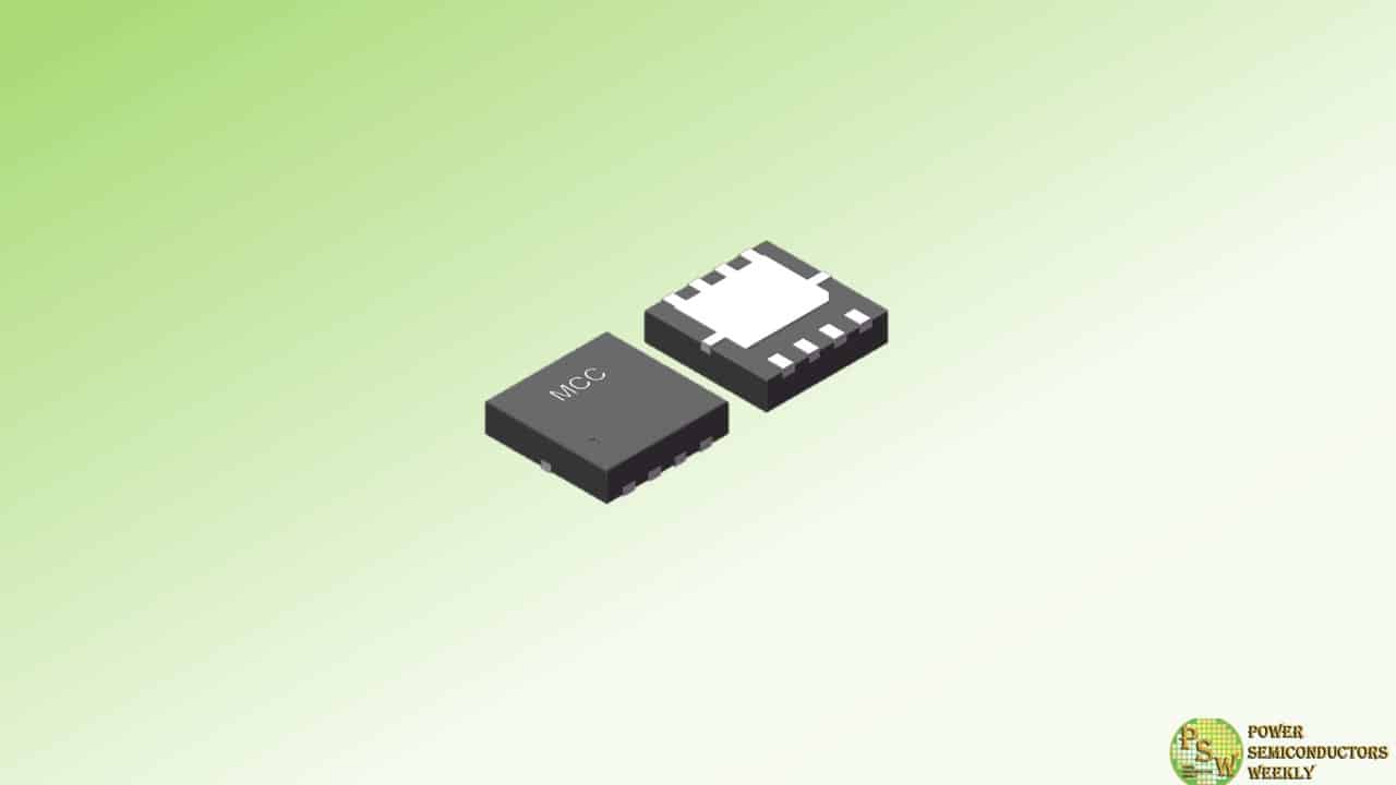
MCC Semi expands its automotive MOSFET portfolio with the addition of four side-wettable flank components. Available in N-channel and P-channel options, these products deliver high power density in a compact DFN3333 package.
Full AEC-Q101 qualification is just one way these MOSFETs ensure quality and reliability. Side-wettable flanks enable more reliable soldering during PCB assembly and allow manufacturers to perform automated optical inspections (AOI) to reduce costs while maintaining quality assurance.
The P-channel MOSFETs MCGWF20P06YHE3 and MCGWF45P04HE3 leverage trench low-voltage (LV) technology and feature RDS(on) from 13mΩ to 26mΩ. And the N-channel solutions MCGWF60N04YHE3 and MCGWF60N06YHE3 utilize split-gate trench technology with RDS(on) from 3.9mΩ to 6mΩ.
No matter which side-wettable flank MOSFET you choose, you can take advantage of versatility and performance for a diverse array of automotive electronic systems.
Features & Benefits:
- AEC-Q101 qualified
- P-channel powered by trench low voltage (LV) technology
- N-channel powered by split-gate trench (SGT) technology
- Low RDS(on)
- Side-wettable flanks ensure soldering stability
- Automated optical inspection capability for cost-effective production
- Compact yet high power density DFN3333 package
Original – Micro Commercial Components
-
Infineon Technologies AG is strengthening its outsourced backend manufacturing footprint in Europe and announced a multi-year partnership with Amkor Technology, Inc., a leading provider of semiconductor packaging and test services. Both companies have agreed on operating a dedicated packaging and test center at Amkor’s manufacturing site in Porto. Operations are expected to commence in the first half of 2025.
With this long-term agreement, Infineon and Amkor further strengthen their partnership, extending the classical Outsourced Semiconductor Assembly and Test (OSAT) business model. Amkor will expand its facilities in Porto and run the production line, providing dedicated clean room space, and Infineon will provide an onsite team with engineering and development support.
The cooperation further strengthens the European semiconductor supply chain and contributes to making it more resilient – especially for automotive customers. It complements Infineon’s already diversified manufacturing footprint, balancing inhouse and outsourced production capabilities.
”We are pleased to further deepen our partnership with Amkor and will contribute with our engineering and development expertise,” said Alexander Gorski, Executive Vice President and responsible for Infineon’s global Backend Operations.
”Infineon and Amkor are jointly increasing geographical resilience and supply security for our customers. Together, we are strengthening Europe’s importance as a location for semiconductor manufacturing. For 20 years, Infineon has been successfully operating a large service center in Porto, now with more than 600 employees. With the joint manufacturing center, we are becoming even more deeply rooted in Portugal’s excellent semiconductor ecosystem. We are looking forward to further increasing our footprint in Portugal.”
“Amkor is proud to expand our partnership with Infineon,” said Giel Rutten, Amkor’s president and chief executive officer. “We continue to invest in our Porto manufacturing site, expanding capacity as well as broadening our Advanced packaging and test technology portfolio. This collaboration represents another milestone for both companies in enhancing supply chain resiliency for advanced products supporting Automotive & Industrial end markets.”
Original – Infineon Technologies
-
Innoscience Technology welcomes, with thanks, two additional decisions, from March 26, 2024, by the United States Patent and Trademark Office (USPTO) to institute review of the validity of yet another two (and still additional) U.S. patents of Efficient Power Conversion Corporation (“EPC”).
The two additional U.S. patents, which are now under review at the USPTO, were previously asserted by EPC at the beginning of the legal dispute initiated by EPC in the U.S. International Trade Commission (ITC). During the course of that proceeding, however, EPC withdrew these patents, but Innoscience maintained its challenges of these patents at the USPTO.
In the March 26, 2024 decisions, the USPTO decided to institute the review of the validity of these two further U.S. patents, as previously asserted by EPC in the ITC proceeding. These new decisions to institute now supplement two other and prior decisions to institute by the USPTO, relating to the other two patents that are still asserted by EPC at the ITC.
Now, in all four decisions, the USPTO has concluded that “there is a reasonable likelihood that Petitioner [Innoscience] would prevail with respect to at least one of the claims challenged in the Petition.” Innoscience has achieved, via the preliminary decisions, a perfect 4-for-4 record at the USPTO.
Also, now all patents that were asserted by EPC now are under review by the USPTO. These new March 26, 2024 rulings by the USPTO are only the latest developments related to EPC’s misguided lawsuits against Innoscience, wherein EPC continues to struggle in its meritless attacks on Innoscience. In all four rulings now, including from March 20 and March 26, 2024, three judges from the USPTO have initially agreed with Innoscience, that the EPC patents that Innoscience challenged at the USPTO are invalid.
And, once again, in this new set, Innoscience again argued to the USPTO that the challenged EPC patent was invalid, based on a prior patent of an EPC cofounder/inventor when he was at International Rectifier, and on a preliminary basis, according to the institution decision, the USPTO agreed with Innoscience. In all four proceedings, Innoscience has described multiple reasons why the four EPC patents are invalid, and for virtually every argument on invalidity, the USPTO initially agreed. Next, the USPTO will receive additional briefing and make final determinations by March 26, 2025.
Innoscience is confident that it will achieve an eventual complete victory in the dispute with EPC. With these recent USPTO decisions of March 26, 2024, Innoscience continues to achieve successes in its legal dispute with EPC, and the additional USPTO decisions repeatedly demonstrate that EPC’s accusations against Innoscience lack merit, given that the USPTO has now determined, at least initially, that all four EPC patents asserted by EPC are likely invalid.
Original – Innoscience Technology
-
SMC Diode Solutions, a leading designer and manufacturer of silicon carbide and silicon die, wafer and packaged products, announced a representative agreement with Atlantic Tech Marketing LLC. The agreement authorizes Atlantic Tech Marketing LLC to promote, sell, and market SMC’s extensive range of discrete products in several US states, including Alabama, Georgia, North Carolina, South Carolina, Mississippi, and Tennessee.
Learn more about Atlantic Tech Marketing LLC here: https://atlantic-tech.com
SMC Diode’s SiC and Si products are sold for a variety of applications in the commercial market including automotive, LCD displays, telecom equipment, power supplies, industrial and aircraft industries, which have demanding reliability and quality requirements.
Original – SMC Diode Solutions
-
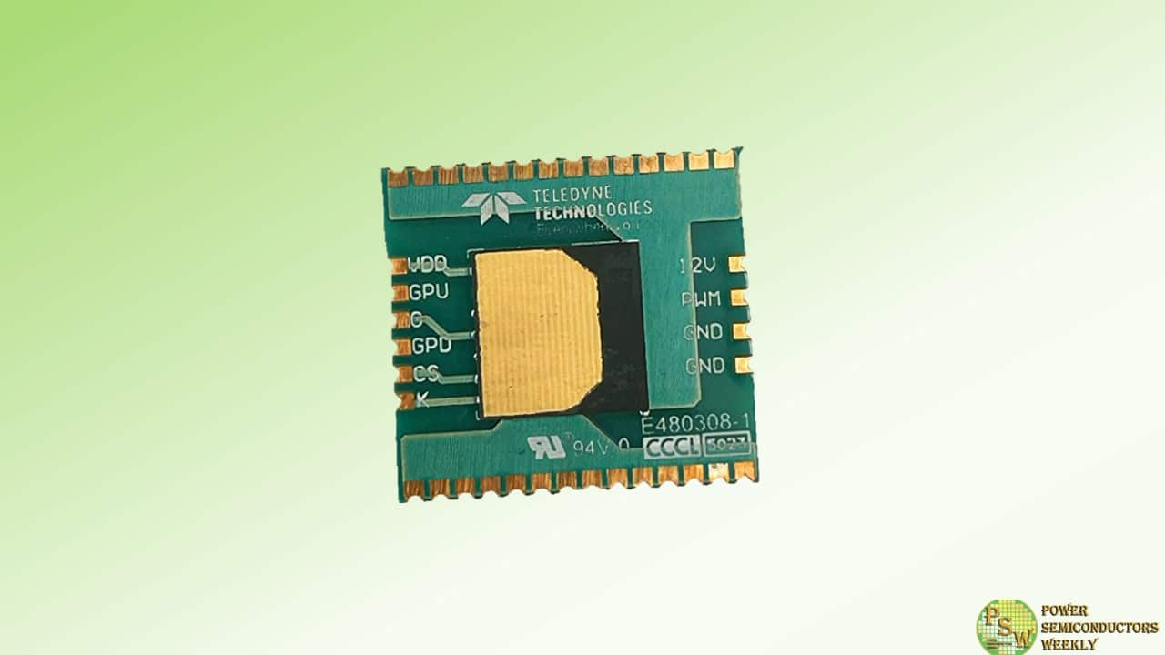
Teledyne e2v HiRel Electronics announced the release of the TDGM650LS60, the first product in its innovative new 650V power module family. This new module utilizes a Teledyne high voltage Gallium Nitride (GaN) transistor and integrates an isolated driver in one package.
Designed to serve as a load switch or solid-state switch, the TDGM650LS60 offers unparalleled performance and versatility. With the driver providing 5KV isolation and a GaN transistor boasting a minimum breakdown voltage of 650V, this module ensures robust and dependable operation in diverse environments.
One of the standout features of the TDGM650LS60 is its lightning-fast switching time coupled with the absence of moving parts. This unique combination not only enhances operational efficiency but also significantly elevates the reliability of the device. As a result, the TDGM650LS60 is ideally suited for high-reliability applications, including but not limited to Space, Avionics, and Military sectors.
“This launch marks a significant milestone in Teledyne’s commitment to innovation” said Mont Taylor, Vice President and Business Development Manager at Teledyne e2v HiRel. “The TDGM650LS60 represents the culmination of our dedication to pushing the boundaries of technology, offering our customers performance, reliability, and versatility in their applications.”
Original – Teledyne e2v HiRel Electronics
-
SemiQ will showcase its latest portfolio of advanced SiC modules at this year’s International Electric Vehicle Symposium & Exhibition (EVS37) in Seoul, South Korea, from April 23rd to 26th, 2024.
Visitors to SemiQ’s booth #C1414 in Hall C, Coex, will have the chance to explore the company’s cutting-edge QSiC™ technologies, including the very latest 1200V SiC modules. Engineered to excel even in demanding environments, these modules facilitate top-tier performance and compact integration, all while mitigating both dynamic and static losses. Crafted from premium-grade ceramics, the modules come in a variety of configurations, including SOT-227, half-bridge, and full-bridge options.
The latest QSiC MOSFET modules offer versatile support for a wide spectrum of demanding automotive and industrial power applications where efficiency, power density and performance are paramount design considerations. These encompass electric vehicle charging, on-board chargers (OBCs), DC-DC converters, electronic compressors (E-compressors), fuel cell converters, medical power supplies, energy storage systems, solar and wind energy applications, data center power supplies, and UPS/PFC circuits.
“We’re excited to show visitors to EVS37 how our QSiC™ family of 1200V MOSFET modules can empower engineers in renewable energy, automotive, medical and industrial sectors,” said Dr. Timothy Han, President of SemiQ. “With rigorous testing and meticulous customization, we guarantee that each module exceeds the requirements of high-efficiency, high-power applications, enhancing reliability and performance.”
EVS37 is a global forum conceived to highlight industry breakthroughs and electric vehicle advancements. Boasting insightful talks by prominent figures from both industry and academia, EVS is a state-of-the-art exhibition featuring contributions from around the world and many opportunities for professional networking.
Original – SemiQ
-
SemiQ has opened its newest office in Taiwan. This strategic move underscores SemiQ’s commitment to providing enhanced ground support to its valued customers in the region while further solidifying its presence in the Asia-Pacific market.
As a Product Engineering and Global Sourcing Center, the new office, located near the Taiwan High Speed Rail Hsinchu Station, will serve as a vital hub, facilitating seamless interfacing with key stakeholders including Hsinchu Foundry, Miaoli Test Facility, Far East OSATs, and Taiwan Sales Office.
“Expanding our presence in Taiwan represents a significant milestone for SemiQ as we continue to strengthen our global operations and better serve our customers,” said Michael Tsang, VP, Product Engineering and Operations at SemiQ. “The opening of this office underscores our dedication to providing unparalleled support and resources to our customer base in the region.”
Mr. Tsang, a seasoned professional with extensive experience in semiconductor industry dynamics, will lead the Taiwan office. His expertise will be instrumental in managing demand, fostering partnerships, and ensuring the highest level of service delivery to SemiQ’s customers.
The strategic location of the new office near key industry players and transportation hubs will enhance SemiQ’s ability to collaborate effectively with its partners, streamline operations and expedite response times to customer needs.
“We are excited about the opportunities that the Taiwan office brings in terms of strengthening relationships with our partners and better understanding the evolving needs of the market,” added Mr. Tsang. “This expansion aligns with our vision of driving innovation and delivering value-added solutions to our customers.”
Establishing the Taiwan office complements SemiQ’s existing wafer processing facilities in the region. It underscores its commitment to providing superior SiC solutions for ultra-efficient, high-performance, and high-voltage applications.
Original – SemiQ
-
Microchip Technology Incorporated announced that its Board of Directors has appointed Rich Simoncic as Chief Operating Officer. In this position, Mr. Simoncic will report to Ganesh Moorthy, who will remain President and CEO.
Rich Simoncic joined Microchip as a new college graduate in 1989 and has had progressively increasing product development, operational and business unit responsibilities. He founded the analog business at Microchip in 1998 and has been instrumental in building it to a more than $2 billion annual revenue business through a combination of organic efforts as well as acquisitions.
He was promoted to Vice President in 1995, Corporate Vice President in 2001, Senior Vice President in 2019 and Executive Vice President in 2023. He holds a Bachelor’s degree in Electrical Engineering Technology from DeVry Institute of Technology.
“Rich has expanded his role over the last few years, beyond leading our analog businesses, by assisting me with several corporate initiatives, including strategic planning, acquisitions, total system solutions, market megatrends, use of artificial intelligence within Microchip and Investor Relations activities. Going forward, Rich and I will jointly manage the worldwide Microchip enterprise so that we can apply our combined leadership capacity to engage the opportunities and challenges ahead of us,” said Ganesh Moorthy, Microchip’s President and CEO.
Original – Microchip Technology
