-

According to the information on the official website of the China National Intellectual Property Administration (CNIPA) on April 2, 2024, the key claims 6, 9, 10, 13, 14, 17, 18 and 22-26 of the Chinese patent titled “Enhancement mode GaN HEMT device and method for fabricating the same” (Patent No. ZL201080015388.2) owned by Efficient Power Conversion Corp (“EPC”) have been maintained valid during an invalidation procedure (case number: 4W116775), which was requested by the petitioner Innoscience (Suzhou) Technology Co., Ltd. (“Innoscience”).
As compared with products using silicon-based devices, transistors and integrated circuits using GaN-based technology are superior in terms of higher efficiency, reduced weight and lower cost. The key claims which are held valid as mentioned above cover core technologies of the design and the manufacturing process of EPC’s proprietary enhancement-mode GaN-based power semiconductor devices. By virtue of multiple innovations including such technologies, EPC has successfully brought GaN-based power devices from laboratory to market.
In May 2023, EPC filed complaints before the US Federal Court and the US International Trade Commission (ITC), asserting that Innoscience (Zhuhai) Technology Co., Ltd. and its affiliate Innoscience infringed four patents of its foundational patent portfolio, which include the US counterpart of this Chinese patent ZL201080015388.2. As part of the responses to those complaints, Innoscience filed, in September 2023, a request to invalidate the EPC’s Chinese counterpart patent ZL201080015388.2 before the CNIPA.
Pursuant to the Chinese Patent Law, Innoscience may appeal this invalidation decision before the Beijing Intellectual Property Court within three months.
Original – Efficient Power Conversion
-

Axcelis Technologies, Inc. announced a shipment of the Company’s Purion EXE™ SiC high energy implanter as well as a successful Purion H200™ SiC medium energy implanter evaluation closure at leading power device chipmakers located in Japan. The systems will be used for 150mm and 200mm production of silicon carbide power devices supporting automotive, industrial, energy, and other power intensive applications.
Greg Redinbo, Executive Vice President, Marketing and Applications remarked, “The successful evaluation closure of the 200mm Purion H200 SiC system enables it to join an existing 200mm Purion EXE SiC in production at a leading power device customer in Japan.” Dr. Redinbo continued, “The shipment of an additional Purion EXE SiC to a new 150mm customer in Japan highlights growing customer requirements for even higher energy ion implant recipes on advanced SiC power devices, which the Purion Power Series provides.”
President and CEO, Russell Low commented, “We look forward to supporting our growing installed base in Japan and remain focused on expanding our market share by providing customers with the most innovative implant technology and support solutions to ensure their success. The Purion Power Series is the market leader due to its highly differentiated features and process control capabilities that are enabling for power device applications. Axcelis is the only ion implant company that can deliver complete recipe coverage for all power device applications.”
Original – Axcelis Technologies
-

Aehr Test Systems announced it has received an initial customer order for a FOX-NP™ wafer level test and burn-in system, multiple WaferPak™ Contactors, and a FOX WaferPak Aligner to be used for engineering, qualification, and small lot production wafer level test and burn-in of their silicon carbide devices.
The customer is multiple billion dollar per year global semiconductor company with locations across Europe, Asia, and the Americas that serves various industries including automotive, industrial, mobile, and consumer applications. The FOX-NP system, including the FOX WaferPak Aligner and initial WaferPaks, are scheduled to ship over the next few months.
The FOX-NP system is configured with the new Bipolar Voltage Channel Module (BVCM) and Very High Voltage Channel Module (VHVCM) options that enable new advanced test and burn-in capabilities for silicon carbide power semiconductors using Aehr’s proprietary WaferPak full wafer Contactors.
Gayn Erickson, President and CEO of Aehr Test Systems, commented, “We are very excited that this new customer selected our FOX-P solution for engineering, qualification, and production of their silicon carbide power devices. After working with the Aehr team and our technology solutions over an extended period of time, they felt secure in our ability to aid them in achieving these goals. A key feature in their selection of our FOX solution is its proven ability to cost-effectively implement their target burn-in and stabilization requirements, including 100% traceability and proof that every device on the wafer is burned in for the needed test duration.
“This customer currently has a wide range of automotive products and is entering the silicon carbide market to address several applications that include automotive, industrial, and electrification infrastructure. Key capabilities of our solution include our ability to scale from engineering and qualification and small lot production with the FOX-NP system to large scale production with the FOX-XP with Automated WaferPak Aligner. They have told us that they plan to transition to our FOX-XP multi-wafer test and burn-in systems for high-volume production. Aehr’s FOX-P technology facilitates a seamless transition from engineering to high-volume production with 100% compatibility between systems.
“This customer sees the enormous opportunity for silicon carbide power devices in industrial and power applications. William Blair forecasts that in addition to the 4.5 million six-inch equivalent wafers that will be needed to meet the demand for electric vehicle related silicon carbide devices in 2030, another 2.8 million wafers are needed to address industrial, solar, electric trains, energy conversion and other applications in 2030. The cost of ownership of our solution proves to be more cost-effective and efficient for these devices than package part burn-in after the die are packaged. This is a strong testimony of the advantage of wafer level burn-in as a better alternative to package part burn-in.
“The FOX family of compatible systems including the FOX-NP and FOX-XP multi-wafer test and burn-in systems and Aehr’s proprietary WaferPak full wafer contactors provide a uniquely cost-effective solution for burning in multiple wafers of devices at a single time to remove early life failures of silicon carbide devices, which is critical to meeting the initial quality and long-term reliability of the automotive, industrial, and electrification infrastructure industry needs.”
The FOX-XP and FOX-NP systems, available with multiple WaferPak Contactors (full wafer test) or multiple DiePakTM Carriers (singulated die/module test) configurations, are capable of functional test and burn-in/cycling of devices such as silicon carbide and gallium nitride power semiconductors, silicon photonics as well as other optical devices, 2D and 3D sensors, flash memories, magnetic sensors, microcontrollers, and other leading-edge ICs in either wafer form factor, before they are assembled into single or multi-die stacked packages, or in singulated die or module form factor.
Original – Aehr Test Systems
-

Novel Crystal Technology (NCT), a global leader in Gallium Oxide (Ga2O3) technology, has successfully grown the first 6-inch Ga2O3 single crystal using the advanced Vertical Bridgman (VB) technique. This achievement marks a significant step forward in NCT’s efforts to deliver larger, high-quality semiconductor wafers for Ga2O3-based power devices.
The VB technique offers several advantages over NCT’s existing Edge-defined Film-fed Growth (EFG) method. By growing the crystal in a cylindrical shape, VB significantly reduces costs associated with substrate cutting. Additionally, it allows for production of substrates in various crystalline orientations, unrestricted by limitations imposed by crystal anisotropy.
Furthermore, the controlled thermal environment of VB growth leads to superior crystal quality with minimal defects, compared to EFG. Finally, dopant uniformity within the substrate is expected to improve, aligning with industry standards for other semiconductors like silicon.
NCT carried out a comparative evaluation between VB and EFG crystals with National Institute of Advanced Industrial Science and Technology (AIST) revealed a dramatic improvement in crystal quality. Synchrotron radiation X-ray topography analysis confirmed minimal defects in the VB-grown crystal, compared to the high density of defects observed in the EFG-grown crystal. This clearly demonstrates the superiority of the VB technique for producing high-quality Ga2O3 substrates.
Ga2O3 is a promising material for power electronics due to its ability to significantly reduce power loss compared to commonly used Silicon Carbide (SiC) in high-voltage applications, like electric vehicles and renewable energy systems. Its wide bandgap characteristics hold immense potential for energy conservation and CO2 emission reduction.
Established in 2015, NCT manufactures 2-inch and 100 mm gallium oxide (Ga2O3) substrates and epi-wafers for power devices. These are commercially available and used by universities, institutes, and power device companies worldwide. NCT currently supplies thousands of these substrates annually to support research and development efforts.
NCT is actively developing larger substrates such as 6-inch. Beyond substrates, NCT has a vision for broader Ga2O3 device production. They are already offering samples of their first Ga2O3 Schottky Barrier Diode, with qualification tests expected to be completed in September 2024.
The development of the Vertical Bridgman growth technique for Ga2O3 single crystals was initiated by Shinshu University, successfully achieving growth of 2-inch and 4-inch crystals. NCT acquired and extended their techniques to enable larger diameter crystal development. This research and development program was partially funded by the Adaptable and Seamless Technology Transfer Program through Target Driven R&D (A-STEP) of the Japan Science and Technology Agency (JST).
Original – Novel Crystal Technology
-
Abstract
The silicon carbide (SiC) inverter brings great advantages to the motor drive systems of new energy vehicles; however, severe challenges to the bearings also happen. The high dc bus voltage and switching frequency of SiC inverter can increase the discharge frequency and energy when the bearing grease film collapses.
As a result, the bearing suffers severe electric corrosion, and the service life of the motor drive system can be shortened. In this paper, the characteristics of common-mode voltage and bearing voltage are analyzed, firstly under space vector pulse width modulation (SVPWM). After that, the common-mode equivalent circuit model of the motor drive system is established. The frequency characteristics of bearing voltage are revealed, and the safe working area is determined.
Then, the frequency characteristics of bearing voltage and current are verified based on IGBT and SiC inverters in experiments. After that, by designing a common-mode filter, the bearing voltage and current are significantly attenuated. Furthermore, the active zero state PWM (AZSPWM) is adopted to reduce the common-mode voltage from the inverter.
At the same time, combined with the common-mode filter, the bearing voltage and current are further reduced. The experimental results show that the switching frequency has a decisive effect on the amplitude of bearing voltage and current. The bearing voltage can be attenuated to around half of the reference bearing voltage by using the common-mode filter and AZSPWM strategy, respectively. T
he combination of the common-mode filter and AZSPWM strategy can reduce the bearing voltage to around one-fourth of the reference bearing voltage, which can effectively reduce the breakdown time and discharge energy of the grease oil film.
1. Introduction
The bearing is the key component which determines the life and reliability of the motor drive system. Motor failures are largely attributed to damage to the bearing, and electric corrosion is one of the main factors. Considering the complexity and cost, the three-phase, two-level voltage source inverter is mainly adopted in the electric vehicle drive system.
The common-mode voltage of the inverter couples through the parasitic capacitances of the motor, resulting in bearing voltage on both sides of the bearing lubricating grease oil film. When the bearing voltage exceeds the breakdown threshold of the lubricating grease oil film, the discharge phenomenon occurs, leading to the electric discharge machining (EDM) bearing current.
The energy released during the discharge can cause concave pits on the surface of inner and outer rings as well as on the rolling balls of the bearing. A large number of breakdown discharges can cause great damage to the bearing, posing a serious threat to the life of the motor drive system.
The 800 V dc bus voltage and SiC power devices are becoming the development direction for electric vehicle drive systems. The high voltage and high frequency are conducive to the reduction in the volume and the improvement of the power density of motor drive systems. For example, in 2022, Marelli Europe S.p.A., a well-known auto parts supplier, developed a high power density SiC inverter with a dc bus voltage of 900 V and a switching frequency of 65 kHz.
Compared with the traditional IGBT inverters, its volume and weight were reduced by 30%, the loss was reduced by 50%, and the efficiency reached 99.5%. The National New Energy Vehicle Technology Innovation Center also developed an SiC inverter with a dc bus voltage 900 V in 2022, with the capacity of 550 kVA and a switching frequency of 25 kHz. Compared with the traditional design, the volume was reduced by 6.6 times, and the weight was reduced by 3.3 times.
However, the increase in dc bus voltage and switching frequency could exacerbate the bearing electric corrosion. Bearing electric corrosion has become a pain point problem that needs to be solved urgently in the field of electric vehicles.
From current research, it could be summarized that the suppression of the motor bearing current can be addressed from three aspects, including the bearing reinforcement, the capacitive coupling paths within the motor, and the source of common-mode voltage. Conductive grease bearings and ceramic bearings have been applied to suppress bearing current. Conductive grease bearings create a conductive channel inside the bearing, bypassing the bearing oil film, making it difficult to establish a stable bearing voltage, which prevents the discharge of the bearing oil film.
However, the metallic particles in the lubricating grease can increase its mechanical wear. Additionally, designing a lubricating grease that balances both lubrication and conductivity poses a technical challenge. Ceramic bearings employ the insulating method to block the current path, increasing the bearing impedance to suppress the bearing current. However, the ceramic bearing can impact the rotor heat dissipation.
Additionally, the accumulated bearing voltage on the shaft still exists, which can create a coupling loop through the non-insulated bearing or gear system of the reducer, still leading to electric corrosion. Ceramic bearings are generally used with the conductive brush to obtain better suppression effect. The conductive brush can release the bearing voltage as much as possible to the housing through a low-impedance path. However, ceramic bearings are relatively expensive, and the conductive brushes require regular maintenance and replacement.
From the perspective of the capacitive coupling paths, it can diminish the capacitive coupling effect to reduce bearing voltage by optimizing the motor design. Additionally, a grounded electromagnetic shielding layer is installed at the end of the stator windings to alter the parasitic capacitive coupling path, thereby suppressing the bearing currents.
However, the suppression effect of bearing currents is relatively small through optimizing windings and slot shapes. Moreover, the electromagnetic shielding layer increases the manufacturing difficulty and the motor cost. The eddy current effect inside the shielding layer leads to an increased temperature, thus reducing its practical application in the industrial field.
The root cause of bearing current lies in the common-mode voltage of the inverter. The amplitude and frequency of the common-mode voltage directly determine the severity of bearing currents. Therefore, by reducing the amplitude of the common-mode voltage at its source, the pressure on bearing design can be significantly alleviated.
The suppression of common-mode voltage can be achieved through both software and hardware methods. Software methods involve the utilization of non-zero vectors modulation strategies, such as AZSPWM, remote-state PWM (RSPWM), near-state PWM (NSPWM), etc. Non-zero vector modulation strategies can reduce the amplitude of common-mode voltage to one-third of that in traditional SVPWM.
The hardware suppression methods mainly include innovative inverter structures, such as multi-level and multi-phase topology circuits, etc. These topologies provide a higher degree of design freedom and can effectively reduce the common-mode voltage when combined with specific modulation strategies. However, considering all factors, including the cost, the power density, and the complexity, the multi-phase and multi-level topologies are less commonly applied in electric vehicles. In addition, the passive filters can also be used to suppress bearing currents thanks to the simple structure.
Unlike IGBT inverters, the SiC inverters have a unique impact on bearing voltage and bearing current. Currently, few studies on motor bearing current under an SiC inverter are available. The high-frequency characteristics of the SiC inverter are more likely to excite parasitic capacitances within the motor, causing complex effects on bearing voltage and bearing current. Moreover, the mechanisms of the bearing voltage and bearing current are not clear, and urgent studies are needed.
This paper aims to reveal the frequency characteristics of bearing voltage and bearing current, and to propose an effective suppression method. In this paper, the characteristics of bearing voltage and bearing current are studied by using IGBT and SiC inverters.
The common-mode equivalent circuit of a motor drive system is established, and the frequency–characteristic curve of bearing voltage is obtained. The principle of dividing the anger zone and safe operating zone of bearing voltage is obtained. The common-mode filter and AZSPWM strategy are adopted to suppress the bearing voltage.
This paper is organized as follows. Section 2 presents the generation mechanism and coupling path of bearing voltage and bearing current. Section 3 presents the high-frequency common-mode equivalent circuit of the motor drive system and the concept of the safe operating zone for bearing voltage. Section 4 describes the experimental platform and test results based on IGBT and SiC inverters. Section 5 presents a suppression method of a common-mode filter to suppress the bearing current. Section 6 presents a suppression method of combining the AZSPWM strategy with the common-mode filter. Section 7 concludes the paper.
2. Bearing Voltage and Bearing Current in Motor Drive System
2.1. Generation Mechanism and Coupling Path
The source of the bearing voltage and bearing current is the high-frequency common-mode voltage output by the inverter. As shown in Figure 1, a three-phase, two-level voltage source inverter comprises of six switch devices, and the common-mode voltage of the inverter Vcm is shown as Equation (1). Vag, Vbg, and Vcg are the three-phase voltages of the inverter to the reference ground g (the inverter heatsink and the motor housing).
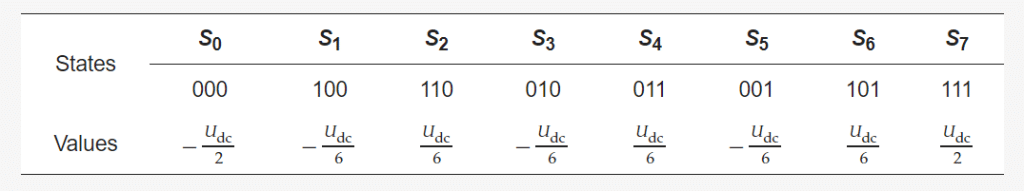
There are eight switch states for the inverter under the SVPWM strategy. The numbers 0 and 1 are utilized to denote the switch states of a bridge arm in an inverter. The state of 1 indicates that the upper device is closed while the lower device is open. The state of 0 indicates that the upper device is open while the lower device is closed. Consequently, the Vcm values of eight switch states are shown in Table 1, while the waveform of Vcm is shown in Figure 2.
In Figure 2, the Udc represents the dc bus voltage and the Ts represents the time of a switching cycle. The common-mode voltage Vcm is a four-level waveform under the SVPWM strategy. In this paper, the impact of switching frequency fs on the common-mode voltage Vcm and bearing voltage Vb is analyzed.

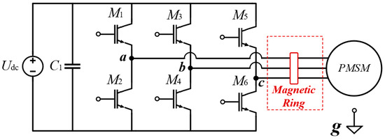
Figure 1. Schematic diagram of the motor drive system.
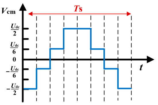
Figure 2. Waveform of common-mode voltage Vcm under SVPWM strategy.
Table 1. Common-mode voltage of the inverter under 8 switch states by using the SVPWM strategy.
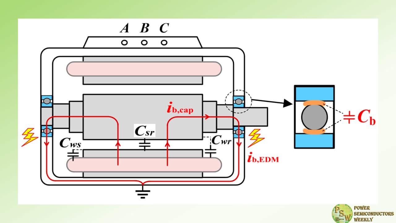
Under the excitation of high-frequency common-mode voltage, the impedance state of the motor exhibits a capacitive characteristic. As shown in Figure 3, Cws, Cwr, and Csr represent the parasitic capacitances of the winding to the stator core and to the rotor, and the stator core to the rotor, respectively. Cb represents the equivalent capacitance of the bearing grease oil film. These parasitic capacitances provide a low impedance coupling path for the high-frequency common-mode voltage.
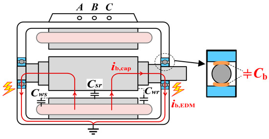
Figure 3. High-frequency parasitic capacitances inside the motor.
The generation process of bearing voltage and bearing current can be described by the equivalent circuit shown in Figure 4. The n point represents the neutral point in the star-connected motor. Vcm represents the common-mode voltage output from the inverter, and Vng represents the common-mode voltage at the motor neutral point. Lc and Rc are the equivalent common-mode inductance and resistance of the cable, respectively, and Lm and Rm are the equivalent common-mode inductance and resistance of the motor winding, respectively. The Rb is the equivalent resistance of the bearing, and Sb is the analog switch in the circuit.
After passing through the cable and the motor winding, Vcm generates Vng at the neutral point of the motor. Under the coupling effect of parasitic capacitances in the motor, a stable bearing voltage Vb is formed at both ends of the bearing lubricating grease film. At this time, the switch Sb in Figure 4 is open, and the change in bearing voltage regularly charges and discharges the oil film capacitance Cb to form the dv/dt capacitive bearing current ib,cap. The amplitude of ib,cap is small, and its influence on bearing electric corrosion is generally ignored.
When the Vb exceeds the voltage threshold of the lubricating grease oil film, the discharge phenomenon occurs. At the discharge moment, the oil film is no longer stable and the Vb drops to 0 V. At this time, the analog switch Sb in Figure 4 is closed, and Cb is shorted to simulate the breakdown and discharge process of the oil film.
The bearing current generated by the discharge is called EDM bearing current ib,EDM. The amplitude of ib,EDM is large, and the energy is released instantaneously. The heat released by multiple discharges could melt the rolling elements and raceways, which is the most direct cause of bearing electric corrosion. According to the above analysis, although the coupling paths of ib,cap and ib,EDM are the same, they do not occur simultaneously.
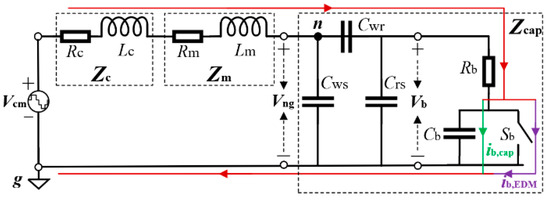
Figure 4. Common-mode equivalent circuit of a motor drive system.
2.2. Analytical Calculation Process
According to the common-mode equivalent circuit shown in Figure 4, the Vng is obtained as shown in Equation (2). Zc is the equivalent common-mode impedance of the cable, Zm the equivalent common-mode impedance of the motor winding, and Zcap is the common-mode impedance of parasitic capacitances inside the motor.

Ignoring the bearing resistance Rb, which is generally very small, the relationship between Vb and Vng is shown in Equation (3). KBVR is defined as the bearing partial pressure ratio, which is often used to roughly evaluate the electric corrosion degree of the bearing. When the bearing is in a stable rotating state, the bearing oil film thickness is stable. Cb is a constant value and KBVR can be considered as a constant.

According to Equations (2) and (3), the relationship between Vb and Vcm is shown in Equation (4). Vb is the result of the voltage division of Vcm through a common-mode equivalent circuit, and the waveform of Vb is consistent with those of Vcm and Vng, both of which are four-level waveforms. When the amplitude and frequency of Vcm are determined, Vb is decided by the common-mode impedances of the cable and motor, which in turn determines the magnitude of ib,EDM.

The accurate calculation of ib,EDM is very difficult, as it depends on the bearing voltage and the impedance of the bearing lubricating grease oil film. The thickness of bearing oil film highly depends on its speed, load, temperature, and the raceway surface roughness. During the rotation process, the lubricating grease oil film is uneven. When the bearing voltage exceeds the voltage threshold, the oil film would break down and discharge at its weakest position.
Therefore, the occurrence of the ib,EDM can be regarded as irregular, and some studies believe that it is random, following statistical probability. However, it should be noted that the occurrence probability of ib,EDM depends on the stable amplitude of the Vb and increases with the increase in Vb.
3. Analysis Model of a Common-Mode Equivalent Circuit for Bearing Voltage
3.1. Frequency Characteristics Analysis of Bearing Voltage
According to Equation (4), when Vcm is determined, the Vb and ib,EDM are mainly affected by the common-mode impedance of the cable and motor. Therefore, it is necessary to study the frequency characteristics of the common-mode impedance of the motor. The common-mode equivalent circuit in Figure 4 is simplified as shown in Figure 5, where Rcm, Lcm, and Ccm are the equivalent resistance, the inductance, and capacitance of the simplified common-mode circuit, respectively.
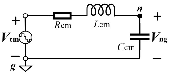
Figure 5. Simplified common-mode equivalent circuit of a motor drive system.
Based on the RLC series equivalent circuit in Figure 5, the variation law of Vng can be obtained by analyzing the voltage frequency characteristics of Ccm. According to Equation (3), the voltage frequency characteristics of Vb are consistent with Vng, so the amplitude–frequency characteristics of Vb can be obtained, as shown in Equation (5).
After the dc bus voltage of the inverter is determined, the Vcm amplitude is determined and the relationship between the Vb and frequency is obtained, as shown in Equation (6). The corresponding frequency–characteristic curve is shown in Figure 6. The P denotes the peak point, and the O denotes the resonant point of the curve in Figure 6. The ωP and ω0 are angular frequencies at points P and O, respectively.

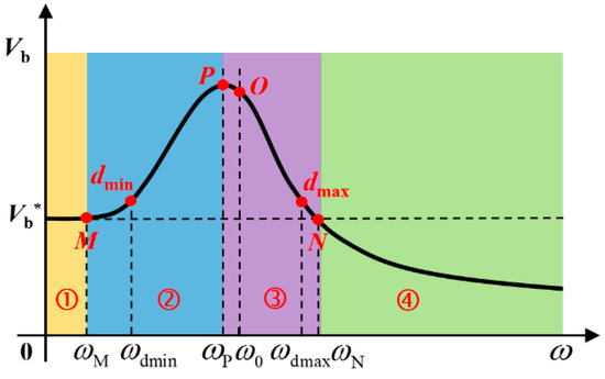
Figure 6. Frequency–characteristic curve of bearing voltage Vb.

In zone ① in Figure 6, the amplitude of Vb remains basically unchanged, and the Vb in this zone is defined as the reference bearing voltage Vb*. The point N is defined as the bearing voltage attenuation point, and the corresponding amplitude is also Vb*. The angular frequency ωN of point N is obtained as follows:

3.2. The Danger Zone and Safe Operating Zone of Bearing Electric Corrosion
As illustrated in Figure 6, the variation trend of Vb is associated with the system common-mode impedance parameters and switching frequency. With the increase in switching frequency, the amplitude of Vb shows a trend of first rising and then decreasing. The frequency–characteristic curve in Figure 6 is divided into four zones. The analysis of each zone is as follows:(1)
Zone ①: the frequency of common-mode excitation is before the ωM. With the increase in frequency, the amplitude of Vb increases slowly and the frequency dependence of Vb is low. This zone is defined as the bearing voltage stable zone. There is Vb ≈ Vb* in this region. The Vb is usually in this zone when the motor is driven by an IGBT inverter (typical switching frequency between 2 kHz and 8 kHz).(2)
Zone ②: the frequency of common-mode excitation is between ωM and ωP, and the amplitude of Vb increases significantly with the increase in frequency. This zone is defined as the bearing voltage growth zone. In this zone, there is always Vb > Vb*, and the Vb reaches its peak value at point P.(3)
Zone ③: the frequency of common-mode excitation is between ωP and ωN, and the amplitude of Vb decreases gradually with the increase in frequency. This zone is defined as the bearing voltage drop zone. In this zone, there is always Vb > Vb*, and Vb decreases to Vb* at point N. However, the amplitude of Vb is still large in this zone.(4)
Zone ④: when the frequency of common-mode excitation exceeds the ωN, Vb begins to decrease below Vb*, and the rate of decline gradually slows down with the increase in frequency. This zone is defined as the bearing voltage safety attenuation zone. In order to reduce the risk of bearing electric corrosion, it is hoped that the switching frequency of the inverter is located in this zone.
In order to better evaluate the impact of bearing voltage on bearing electric corrosion, the zone in Figure 6 where Vb ≥ 1.1 Vb* is defined as the bearing electric corrosion danger zone. According to Equation (6), the expressions of ωd_min and ωd_max of, respectively, the lower and upper frequency points in this zone are as follows:

In order to avoid the risk of bearing corrosion, the selection of switching frequency should try to avoid the danger zone between dmin and dmax in Figure 6. However, the selection of switching frequency is determined by many factors, such as efficiency, volume, power density, electromagnetic interference performance, etc. Therefore, the curve in Figure 6 can provide some references for the selection of the switching frequencies of SiC inverters.
Compared with other zones, zone ④ can obtain a smaller amplitude of Vb. Driven by a traditional IGBT inverter, Vb is often in region ①. However, the SiC device increases the switching frequency of the inverter, causing Vb to be located in zones ② or ③ with a large amplitude. This will increase the frequency and the harm degree of the EDM bearing current, causing serious bearing electric corrosion.
4. Experimental Measurement of Bearing Voltage and Bearing Current
4.1. Experimental Platform and Measurement Methods
The experimental platform is established as shown in Figure 7. An embedded permanent magnet synchronous motor is adopted with 6007 deep groove ball bearings. The bearing manufacturer is SKF, a company headquartered in Gothenburg, Sweden. The rotor materials are permanent magnets and silicon steel sheets. The electrical parameters of the motor are shown in Table 2.
The motor is driven by an IGBT inverter or a SiC inverter, with rated powers of 10 kW, respectively. The IGBT inverter is purchased from KEB, a company headquartered in Barntrup, Germany. The SiC inverter is developed in-house in the laboratory. The bearing voltage is measured using a conductive brush. The bearing current is measured through an intrusive measurement method, which requires modification of the motor end cover.
An insulating layer is inserted between the bearing outer race and the motor end cover. Additionally, an external connection is established between the bearing outer race and the motor housing by using a short wire beside the motor for measuring bearing current.
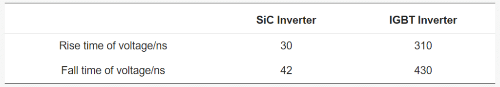
The SVPWM strategy, 400 V bus voltage, and 0.5 m of unshielded cable are used in the experiment. The SiC transistor and the IGBT transistor used in this paper are the C2M0080120D and IGW40N120H3, respectively. The rise and fall times of output voltages for SiC inverter and IGBT inverter are provided in Table 3.
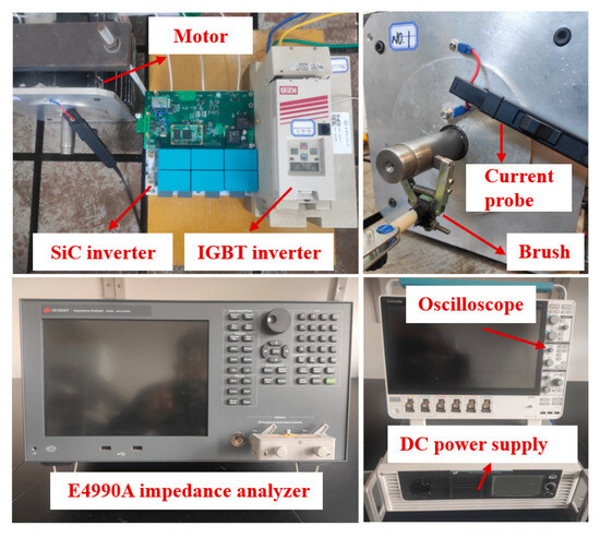
Figure 7. The experimental platform for the bearing voltage and current tests.
Table 2. The electrical parameters of the motor.
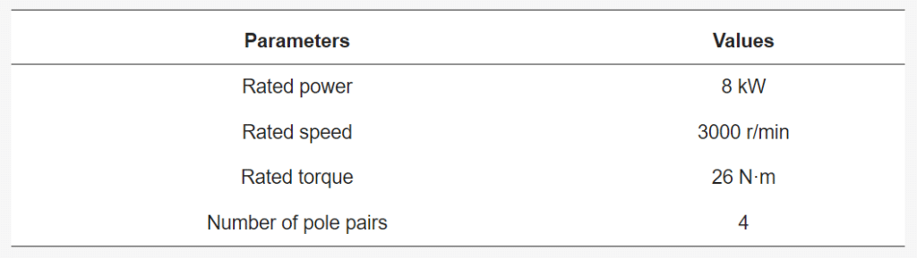
Table 3. The rise and fall times of output voltage for inverters.
For deep groove ball bearings, when the rotational speed is below approximately 300 r/min, the lubricating grease cannot completely envelop the ball, resulting in metal-to-metal contact between the ball and the inner and outer races. The bearing oil film is short-circuited, preventing the establishment of bearing voltage.
When the bearing speed is relatively high, the lubricating grease can generally form a stable oil film, allowing for the establishment of bearing voltage. Therefore, in order to ensure the stable establishment of bearing voltage, the motor speed used in the experiment is set at 1200 r/min with a modulation ratio of M = 0.4 in this paper.
4.2. Experimental Results under IGBT and SiC Inverters Drive
The experimental results of the motor neutral point voltage Vng, bearing voltage Vb, and bearing current were obtained using IGBT and SiC inverters, as shown in Figure 8. ib,de and ib,nde are, respectively, driven-end and non-driven-end bearing currents of the motor, and Tb is the temperature of the bearing outer race. In Figure 8, under the IGBT and SiC inverters’ drive, the stable amplitudes of Vb are approximately Vb_IGBT ≈ Vb_SiC = 6.3 V.
It indicates that the stable amplitude of the Vb is significantly influenced by the switching frequency but is only slightly affected by the switching speed. In Figure 8a, the maximum value of ib,EDM__IGBT is 55 mA, while in Figure 8b, the maximum value of ib,EDM__SiC is 57 mA, with the amplitudes being nearly equal. Different high-bandwidth current probes were employed for repeated testing, revealing that the 2 mA current difference is not measurement error but a real difference.
An explanation of this phenomenon is as follows: when the bearing rotates steadily, the lubricating grease film is uneven, and the raceway roughness is difficult to predict. Consequently, when breakdown discharge occurs in the oil film, the breakdown impedance is also different, which leads to slightly different amplitudes of ib,EDM under the same test conditions.
In the test conditions shown in Figure 8, both IGBT and SiC inverters were used, and a total of 30 sets of ib,EDM were captured in each case. The results show that although the bearing voltage amplitudes are equal, all captured amplitudes of ib,EDM fluctuate around 55 mA, with variations not exceeding 4 mA. This current fluctuation is considered normal and is not a result of measurement error.
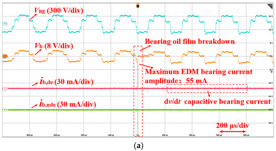
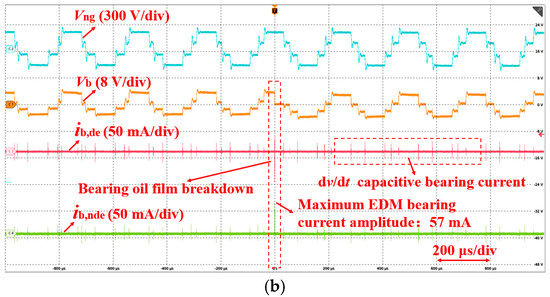
Figure 8. Measured waveforms of Vng, Vb, ib,de, and ib,nde (test conditions: SVPWM, Udc = 400 V, fs = 4 kHz, M = 0.4, Tb: 24~26 °C). (a) Under IGBT inverter drive; (b) under SiC inverter drive.
Since Vb_IGBT and Vb_SiC have similar amplitudes, the maximum amplitudes of ib,EDM__IGBT and ib,EDM__SiC are also approximately equal, indicating that the amplitude of Vb determines the energy of the ib,EDM.
Furthermore, from Figure 8, it can be observed that the capacitive bearing current ib,cap under the IGBT inverter is smaller than that in the SiC inverter, mainly due to the faster switching speed of the SiC inverter compared to the IGBT inverter.
According to Table 3, the switching speed of the SiC inverter is approximately one-tenth of that of the IGBT inverter. The amplitude of ib,cap is small, and the impact on bearing electric corrosion is also small. Under the IGBT inverter drive, ib,cap is generally neglected. However, under the SiC inverter drive, the impact of ib,cap on the bearing electric corrosion currently lacks relevant research conclusions.
4.3. Experimental Verification of Frequency Characteristics for Bearing Voltage and Current
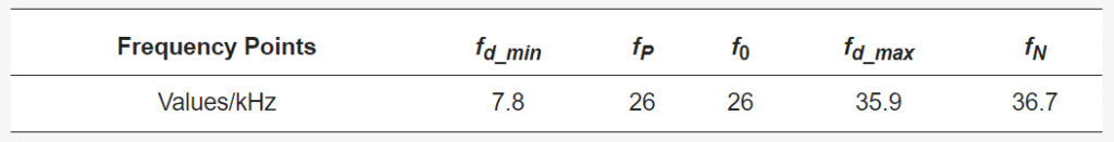
The experimental platform in Figure 7 is used for testing, and the measurement results of common-mode parameters of the motor and cable are obtained, as shown in Table 4. By substituting the parameters into Equations (7)–(11), the theoretical calculation results of points P, O, d_min, d_max, and N in Figure 6 are obtained. as shown in Table 5.
Table 4. The measured parameters of a common-mode equivalent circuit.

Table 5. Theoretical calculation results of frequency points for a Vb characteristic curve in the experimental system.
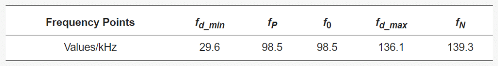
According to Table 5 and Figure 6, the analyses are as follows. When the switching frequency of the inverter used in the experiment exceeds 29.6 kHz, Vb begins to enter the danger zone in Figure 6. As the switching frequency increases, the amplitude of Vb increases significantly, reaching its maximum value at a frequency of 98.5 kHz. In the range from 98.5 kHz to 136.1 kHz, Vb begins to decrease, but it remains higher than the reference bearing voltage Vb*.
Therefore, when the switching frequency falls within the range from 29.6 kHz to 136.1 kHz, there is a significant risk of bearing electric corrosion. According to Figure 6, when the switching frequency exceeds 139.3 kHz, Vb starts to decrease below Vb*. In fact, constrained by electromagnetic interference and the control speed of the main controller, the switching frequency of the SiC inverter for the electric vehicle is generally lower than 100 kHz at present. Therefore, for the motor drive system adopted in the experiment, the Vb is located in zones ① and ② in Figure 6.
The theoretical calculation and experimental results of the Vb under different switching frequencies are obtained in Figure 9. The reference bearing voltage is Vb* = 6.3 V. When the switching frequency is less than 20 kHz, Vb increases slowly. In the range of 20 kHz–80 kHz, Vb increases quickly. Below 40 kHz, the theoretical calculations and experimental results are basically consistent. Above 40 kHz, with the increase in switching frequency, the error between the theoretical calculation and experimental results becomes more significant.
The analyses of error sources are as follows. Although the RLC lumped parameter equivalent circuit of the motor is simple, it is not accurate. In addition, there are measurement errors in the extraction of circuit parameters. Although there are errors at high frequencies, the overall variation trend of the bearing voltage is consistent with that of the frequency–characteristic curve depicted in Figure 6.
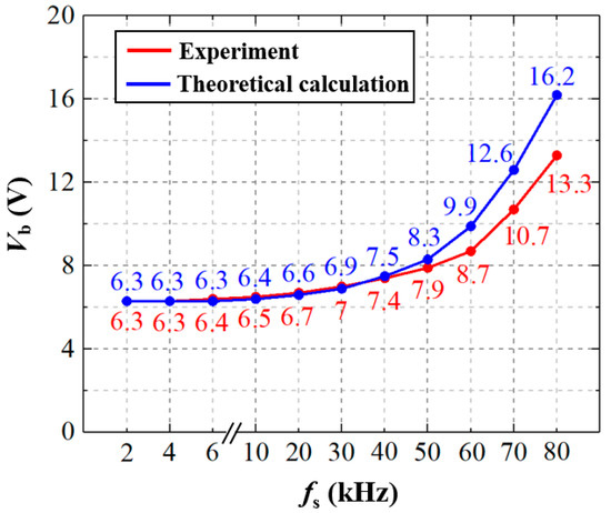
Figure 9. Variation trend of bearing voltage with switching frequency.
Figure 10 shows the number of ib,EDM occurrences (that is, the number of bearing oil film breakdown discharges) with the switching frequency per minute. The number of breakdown discharges was measured by taking the average value of multiple sample datasets. The results show that the increase in Vb could lead to the increased bearing breakdown discharges. The number of ib,EDM is approximately exponential with the rising switching frequency.
Based on Figure 10, the relationship between breakdown discharge times and switching frequency is obtained, as shown in Equation (12). Nd denotes the number of breakdown discharges. For the application in this paper, the values of the variables are A = 16.3, B = 8 × 10⁷, C = 137.9, D = 2, and E = 349.

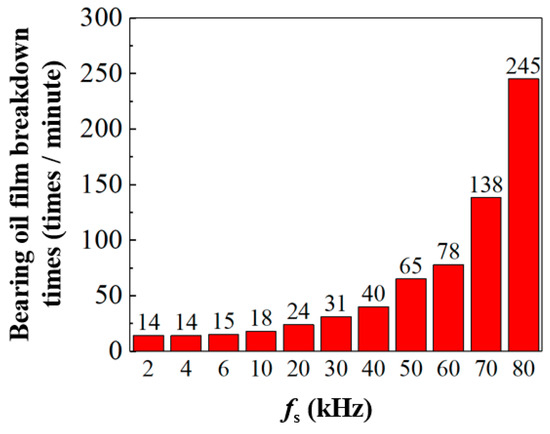
Figure 10. Variation trend of bearing oil film breakdown times with switching frequency.
The basic bearing voltage Vb*, especially at low switching frequency, already poses a significant threat to motor bearings. The increased switching frequency of the SiC inverter inevitably results in a further increase in bearing voltage. The dc bus voltage of the motor drive system is upgraded from 400 V to 800 V, which can double the bearing voltage. Therefore, with the increase in dc bus voltage and switching frequency, bearing voltage, and EDM bearing current are fatal to bearing damage, and effective suppression measures must be taken.
5. Design of Common-Mode Filter for Reducing Bearing Voltage and Current
The high switching frequency of the SiC inverter is advantageous for reducing the volume of the filter. Employing a common-mode filter to improve the frequency characteristics of a common-mode equivalent circuit and to suppress bearing voltage is an effective approach to mitigate bearing electric corrosion.
5.1. Theoretical Calculation and Experimental Verification for Common-Mode Filter
The actual operating frequency of the SiC inverter used in the experiment is 50 kHz. According to Table 5, the Vb of the experimental motor is located in zone ② in Figure 6, which is the danger zone. In order to greatly reduce the Vb, it is necessary to design a common-mode filter to ensure that Vb is located in zone ④, so as to reduce the risk of bearing electric corrosion. The common-mode equivalent circuit of the motor drive system with a common-mode filter is shown in Figure 11.
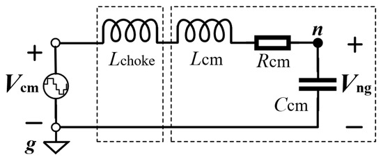
Figure 11. Common-mode equivalent circuit of the motor drive system with a common-mode filter.
In order to attenuate the Vb by at least half of the reference bearing voltage Vb*, according to Equation (6), the Equation (13) can be obtained:

Substituting the parameters in Table 4 into Equation (13), Lchoke ≥ 10.33 mH is obtained. The inductance of common-mode filter needs to be greater than 11 mH. In order to achieve Vb ≤ 0.5Vb*, the actual designed common-mode filter has a certain margin, and the final inductance value is 13 mH.
There is an error in the actual and theoretical design of the inductance value, which mainly arises from the following three aspects: the presence of other harmonic components in the common-mode excitation Vcm, inherent errors in the lumped parameter equivalent circuit, measurement errors in the extraction of common-mode parameters, and parasitic parameters in the filter. The above factors cause the error between the theoretical and actual inductance values in this paper.
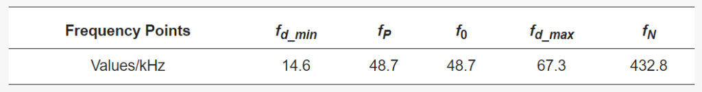
According to the equivalent circuit model shown in Figure 11, when the inductance of the common-mode filter changes, the frequency characteristics of the motor drive system also change accordingly. Correspondingly, the curve of Vb also changes with frequency in Figure 6. According to Equations (7)–(11), the theoretical calculation results of each frequency point at the curve in Figure 6 are shown in Table 6 by using a 13 mH common-mode filter.
Table 6. Theoretical calculation results of frequency points for the Vb characteristic curve in the experimental system (Lchoke = 13 mH).
The experimental waveforms are shown in Figure 12. In Figure 12a, the amplitude of Vb is 7.9 V without a common-mode filter, and the maximum amplitude of ib,EDM is 120 mA. Vb is located in zone ② of Figure 6. In Figure 12b, after using a common-mode filter, the measured amplitude of Vb is 3.1 V, and Vb is located in zone ④ of Figure 6, which is reduced to 0.49 times of the reference value Vb* = 6.3 V. By using a common-mode filter, significant attenuation of Vb is obtained, and no discharge of oil film occurs during the experiment.
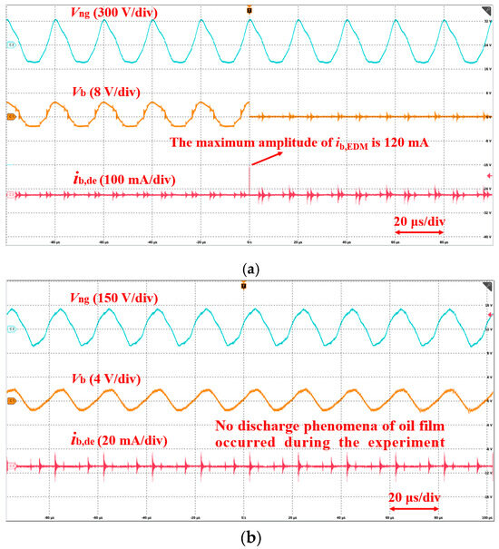
Figure 12. Measured waveforms of Vng, Vb, and ib (test conditions: SVPWM, Udc = 400 V, fs = 50 kHz, M = 0.4, Tb: 24~26 °C). (a) Without common-mode filter; (b) with a 13 mH common-mode filter.
5.2. Negative Effects Caused by Improper Design of a Common-Mode Filter
In order to suppress electromagnetic interference in practical applications, a magnetic ring is often used at the output end of inverter, as shown in the red box in Figure 1. The magnetic ring can be equivalent to a common-mode filter with a single turn coil, which has a small inductance. The Vb is usually located in zone ① of Figure 6 when using an IGBT inverter with a low switching frequency. According to Figure 6 and Equation (6), the amplitude of Vb is basically not increased when the common-mode magnetic ring is installed at the output end of inverter.
Therefore, the magnetic ring is used to suppress electromagnetic interference while minimizing the negative impact on Vb. However, when using a SiC inverter with a high switching frequency, Vb is located in zone ② in Figure 6. If the magnetic ring is still installed at the output end of the inverter to suppress electromagnetic interference, according to Equation (6), Vb would increase significantly, thereby increasing the risk of bearing electric corrosion.
To illustrate the above issue, a common-mode filter with a small inductance of 3 mH is used for the analysis. The frequency points of the curve in Figure 6 are recalculated and the results are shown in Table 7. According to Figure 6 and Table 7, if the inverter still adopts the switching frequency fs = 50 kHz, which is close to the resonant frequency of the system in Table 7, the amplitude of Vb is large. As a result, the bearings will face a significant risk of electric corrosion.
Table 7. Theoretical calculation results of frequency points for the Vb characteristic curve in the experimental system (Lchoke = 3 mH).
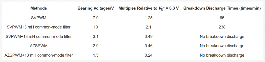
Still using the same testing conditions as in Figure 12, the experimental results are shown in Figure 13. The measured amplitude of Vb reaches 13 V, which is 65% higher than that (7.9 V) in Figure 12a. This significantly increases the breakdown times and discharge energy of the bearing oil film. The number of breakdown discharges per minute measured is as high as 238 times, and the maximum EDM bearing current is 250 mA, which is approximately twice that (120 mA) shown in Figure 12a.
Based on the theoretical and experimental results above, the switching frequency fs = 50 kHz in the experiment is close to the peak point frequency in Figure 6, inevitably leading to excessive bearing voltage and serious bearing corrosion.
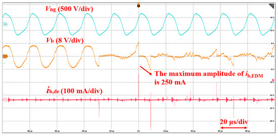
Figure 13. Measured waveforms of Vng, Vb, and ib (test conditions: SVPWM, Udc = 400 V, fs = 50 kHz, M = 0.4, Tb: 24~26 °C, Lchoke = 3 mH).
In summary, for the SiC motor drive system, the design of a common-mode filter or magnetic ring needs to consider the suppression effects on both electromagnetic interference and bearing voltage. It is essential to refer to the design methods proposed in Section 3. Otherwise, improper filter design may exacerbate the bearing electric corrosion.
6. The Suppression Method for Bearing Current in a Motor Drive System with a High-Voltage SiC Inverter
In order to relieve the design pressure of the bearing in the motor drive system with a high voltage and high frequency, the AZSPWM strategy is adopted to weaken the common-mode voltage of the inverter from the source. Then, a common-mode filter is adopted for the output end of the inverter to further reduce the bearing voltage, reducing the discharge times and the discharge energy of the bearing oil film.
6.1. The AZSPWM Strategy
With the SVPWM strategy, the maximum value of the common-mode voltage is Udc/2 when using the zero vector. A non-zero vector modulation strategy can be used to reduce the common-mode voltage amplitude by canceling the zero vector.
Considering the switching loss, modulation ratio, and harmonics, the AZSPWM strategy is adopted in this paper. The comparison of the vector synthesis for SVPWM and AZSPWM-1 in sector I is shown in Figure 14. The idea of AZSPWM-1 is to replace the zero vector by using two non-zero vectors in opposite directions acting at the same time, so that the amplitude of the common-mode voltage is suppressed to Udc/6.
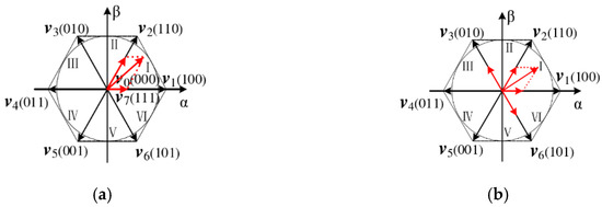
Figure 14. Comparison of vector syntheses for different modulation strategies (taking sector I as an example). (a) SVPWM; (b) AZSPWM-1.
The AZSPWM strategy is divided into three types: AZSPWM-1, AZSPWM-2, and AZSPWM-3. The suppression effect on the common-mode voltage is the same for all three modulation strategies. For AZSPWM-2 and AZSPWM-3, the two bridge arms of the inverter need to operate simultaneously, leading to increased losses. Therefore, the AZSPWM-1 strategy is adopted. The AZSPWM-1 strategy may increase current harmonics, but the high switching frequency of the SiC inverter can reduce these current harmonics, compensating for this drawback.
With the AZSPWM-1 strategy, the common-mode voltage waveform is shown in Figure 15. The amplitudes are different in the even sector and odd sector, but the maximum value is Udc/6, which is one-third of the maximum value Udc/2 under the SVPWM strategy.
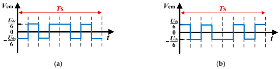
Figure 15. Diagram of common-mode voltage waveform under AZSPWM-1 strategy. (a) Even sector; (b) odd sector.
6.2. The Suppression Effect of Bearing Voltage and Bearing Current
Still using the same testing conditions as Figure 12, the experimental results are shown in Figure 16. In Figure 16a, the AZSPWM-1 strategy is adopted and the amplitude of Vb is reduced to 2.9 V, which is 63% lower than that of 7.9 V driven by SVPWM in Figure 12a. In Figure 16b, the combination of AZSPWM-1 and the 13 mH common-mode filter is adopted. The amplitude of Vb is reduced to 1.5 V and the Vb is greatly attenuated. During the experiment, no discharge phenomena occurred.
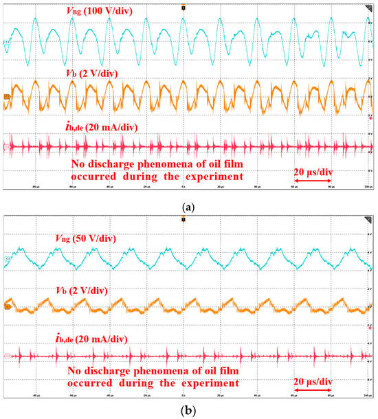
Figure 16. Measured waveforms of Vng, Vb, and ib (test conditions: SiC inverter, AZSPWM-1, Udc = 400 V, fs = 50 kHz, M = 0.4, Tb: 24~26 °C). (a) Without common-mode filter; (b) with a 13 mH common-mode filter.
The comparison results of bearing voltage amplitudes and breakdown discharge times are shown in Table 8 under different suppression methods. The combination of AZSPWM-1 and the common-mode filter achieves the best suppression effect, reducing the bearing voltage to 1.5 V. It effectively suppresses the EDM bearing current and is highly suitable for a motor drive system with a high voltage and high frequency.
Table 8. Comparison results of bearing voltage and discharge times under different suppression methods.
7. Conclusions
This paper investigates the characteristics and suppression methods of bearing voltage and EDM bearing current under SiC inverter drive. By establishing the common-mode equivalent circuit of the motor drive system, the frequency characteristics of bearing voltage are revealed. The suppression method is proposed, which is suitable for a motor drive system with a high voltage and high frequency. Through theoretical analysis and experimental validation, the following conclusions are drawn.
Compared to a traditional IGBT inverter, the SiC inverter with a high switching frequency increases the amplitude of bearing voltage, exacerbating the risk of bearing electric corrosion. The selection of switching frequency must consider the impact on the bearing voltage and the EDM bearing current.
For motor drive systems with a SiC inverter, the design of the common-mode filter or magnetic ring needs to consider the influence on bearing voltage and current. Otherwise, negative effects may occur, aggravating bearing electric corrosion. The proposed design method of common-mode filter can improve the frequency characteristics of bearing voltage, attenuating the bearing voltage to half of the reference bearing voltage and keeping it in the safe operating zone.
The AZSPWM-1 strategy can attenuate the bearing voltage to around half of the reference bearing voltage. When combining AZSPWM-1 and a common-mode filter, the bearing voltage is reduced to around one-fourth of the reference bearing voltage, achieving the best suppression effect. This method effectively reduces the breakdown times of lubricating grease oil film, which is suitable for motor drives with a high voltage and high frequency in electric vehicles.
Authors
Mingliang Yang, Yuan Cheng, Bochao Du, Yukuan Li, Sibo Wang, Shumei Cui.
Original – MDPI
-

Infineon Technologies AG and HD Korea Shipbuilding & Offshore Engineering Co. Ltd. (HD KSOE) have signed a non-binding Memorandum of Understanding (MoU) as a first step towards jointly developing emerging applications for the electrification of marine engines and machinery using energy-efficient power semiconductor technology.
HD KSOE, a marine pioneer and global leader in ship building, is already focusing on creating eco-friendly decarbonized ship technology that uses electricity and hydrogen. The company will now cooperate with Infineon to create innovative power solutions for propulsion drive technology, a core element for ship electrification.
Power semiconductors from Infineon drive the transformation towards clean, safe, and smart mobility services across all means of transportation. For modern maritime applications they are a key factor in guaranteeing a precise control of multiple power modules, such as large-capacity propulsion drives.
Infineon will provide HD KSOE with technical assistance and mentoring in semiconductor power modules and system solutions, as well as share information on new semiconductor trends for marine applications. With the partnership HD KSOE aims to enhance reliability and performance of marine vessels’ propulsion drive technology contributing to environmental sustainability through the electrification of ships.
Worldwide, maritime transport is responsible for almost 2.5 percent of total greenhouse gas emissions, according to the International Maritime Organization. It produces one billion tons of CO 2 each year. The transition to electric ships is imperative to mitigate the environmental impact of maritime transportation.
“We are pleased to sign an MoU with Infineon, which underpins our innovation efforts to become a leader in ship electrification technology,” said Chang Kwang-pil, Chief Technology Officer of HD KSOE. “Together, we will combine our strengths to create energy-efficient power solutions for CO2-friendly propulsion drives.”
“At Infineon we are providing the technologies needed in today’s world of transportation to drive electrification that will shape the future of mobility,” said Dr. Peter Wawer, Division President Green Industrial Power at Infineon Technologies. “We are excited to work closely together with HD KSOE to develop clean, safe and smart mobility solutions. This way, we contribute to a more sustainable marine engine ecosystem and drive the decarbonization of shipping.”
Original – Infineon Technologies
-

CVD Equipment Corporation announced its financial results for the fourth quarter and fiscal year ended December 31, 2023.
Manny Lakios, President and CEO of CVD Equipment Corporation, commented, “Fourth quarter 2023 revenue was $4.1 million, down significantly versus the prior year period, as our business continues to experience fluctuations in revenue given the nature of the emerging growth end markets we serve. While we are disappointed with both our fourth quarter and full year performance, we’ll stay the course on our strategy to return to consistent profitability, with a focus on growth and return on investment.”
Mr. Lakios added, “Our primary goal is to expand penetration of our equipment solutions into high power electronics, battery material, aerospace and industrial applications. To this end, I am very pleased to announce that we started off 2024 with several key new order wins. First, we successfully penetrated a second PVT equipment customer, with an evaluation order for our newly launched PVT200 system used to grow 200 mm silicon carbide crystals. This represents an important milestone for CVD, with potential follow-on production orders should our equipment effectively meet the customers’ needs. Second, we received a $10 million multisystem order for a SiC CVD coating reactor from an industrial customer, which will be used to deposit a silicon carbide protective coating on OEM components. We are encouraged by these orders, as we continue to make investments in both research and development and sales and marketing, including direct engagement with multiple potential customers, focused on our key markets.”
Fourth Quarter 2023 Financial Performance
- Revenue of $4.1 million, down $3.1 million or 43.2% year over year primarily due to lower system revenues.
- Gross profit margin percentage was a negative 8.5% due to a large contract that experienced significant cost overruns during the quarter.
- Operating loss of $2.5 million.
- Net loss of $2.3 million or $0.33 basic and diluted share, compared to a net income of $1.5 million or $0.23 per basic and diluted share during the prior year fourth quarter. Net income in 2022 included $1.5 million of other income related to the recognition of Employee Retention Credits related to fiscal 2021.
- Cash and cash equivalents of $14.0 million as of December 31, 2023.
Full Year 2023 Financial Performance
- Revenue of $24.1 million, down $1.7 million or 6.6% year over year primarily due to the disposition of Tantaline and the wind down of MesoScribe’s operations.
- Our gross profit margin percentage was 21.0% in 2023 as compared to 25.7% in the prior year due to a large contract in 2023 that experienced significant cost overruns and other higher margin system contracts in 2022.
- Operating loss of $4.9 million.
- Net loss of $4.2 million or $0.62 basic and diluted share, compared to a net loss of $0.2 million or $0.03 per basic and diluted share in the prior year. Net loss in 2022 included $1.5 million of other income related to the recognition of Employee Retention Credits.
Fourth Quarter 2023 Operational Performance
- Orders for the fourth quarter were $5.8 million driven by continued demand in the aerospace sector and in our SDC segment for gas delivery equipment.
- Received a $2.1 million system order in the aerospace sector that will be delivered over the next 12 months.
- Received a $1.0 million order in our SDC segment for gas delivery equipment.
- During the fourth quarter, we developed a plan to reduce our operating costs to be consistent with current customer demand. This resulted in a reduction in our work force in early January 2024. We continue to evaluate opportunities to reduce our operating costs.
Full Year 2023 Operational Performance
- Booking of new orders from customers was $25.8 million, representing a decrease of approximately 22.1% compared to 2022 bookings of $33.1 million. The decline in bookings was related to large orders of PVT150 systems that were received in 2022.
- Backlog as of December 31, 2023 of $18.4 million, an increase from $17.8 million from the prior year end.
Original – CVD Equipment
-

Ideal Power Inc. announced the closing of its previously announced underwritten public offering of 2,000,000 shares of its common stock (or pre-funded warrants in lieu thereof) at an offering price of $7.50 per share of common stock.
Titan Partners Group, a division of American Capital Partners, acted as sole book-running manager for the offering.
The gross proceeds to the Company from the offering were approximately $15 million, before deducting underwriting discounts, commissions and other estimated offering expenses payable by the Company. The Company intends to use the net proceeds from this offering for general corporate and working capital purposes.
The offering was made pursuant to an effective “shelf” registration statement on Form S-3 (File No. 333-269060) previously filed with the Securities and Exchange Commission (the “SEC”) on December 29, 2022, and declared effective by the SEC on January 9, 2023. A final prospectus supplement and the accompanying prospectus relating to and describing the terms of the offering were filed with the SEC on March 27, 2024.
Electronic copies of the final prospectus supplement and the accompanying prospectus relating to the offering, may be obtained by visiting the SEC’s website at www.sec.gov or by contacting Titan Partners Group LLC, a division of American Capital Partners, LLC, 4 World Trade Center, 29th Floor, New York, New York 10007, by phone at (929) 833-1246 or by email at prospectus@titanpartnersgrp.com.
Original – Ideal Power
-
 LATEST NEWS
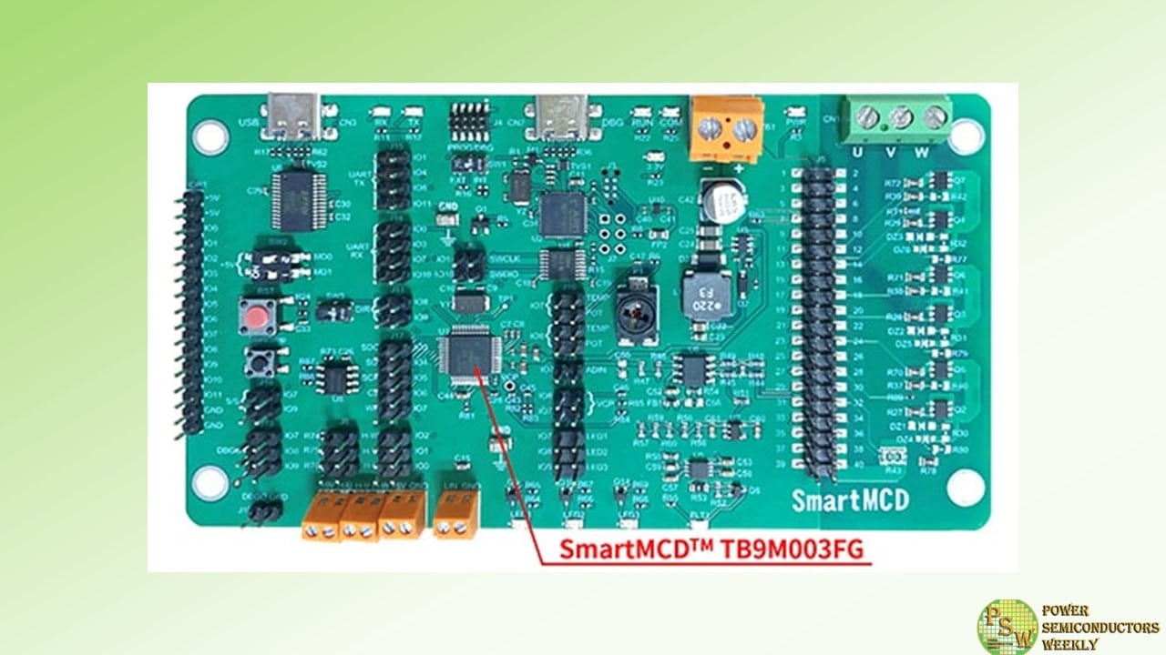
Toshiba Starts Volume Shipments of SmartMCD™ Series of Gate Driver ICs with Embedded Microcontroller
March 28, 2024
2 Min ReadToshiba Electronic Devices & Storage Corporation has started volume shipments of the SmartMCD™ Series of gate driver ICs with embedded microcontroller (MCU). The first product, “TB9M003FG“, is suitable for sensorless control of three-phase brushless DC motors used in automotive applications, including water and oil pumps, fans and blowers.
TB9M003FG combines a microcontroller (Arm® Cortex®-M0), flash memory, power control functions and communications interface functions into a gate driver that controls and drives N-ch power MOSFETs for three-phase brushless DC motor drives.
This integration will reduce system sizes and component counts while realizing advanced and complex motor control for a wide variety of automotive motor applications. The new product also incorporates Toshiba’s proprietary vector engine, hardware for sensorless sinewave control, reducing the load on the microcontroller, and the size of the software.
A reference design using TB9M003FG, “Motor Driving Circuit for Automotive Body Electronics Using SmartMCD™”, is now available on Toshiba’s website.
The expanding market for electric vehicles (xEV) requires electrification, component integration, downsized electronic control unit (ECUs), and quieter motors. In response, the new product contributes to downsizing of ECUs by integrating a microcontroller into the gate driver, and to quieter motors by using vector control.
Original – Toshiba
-
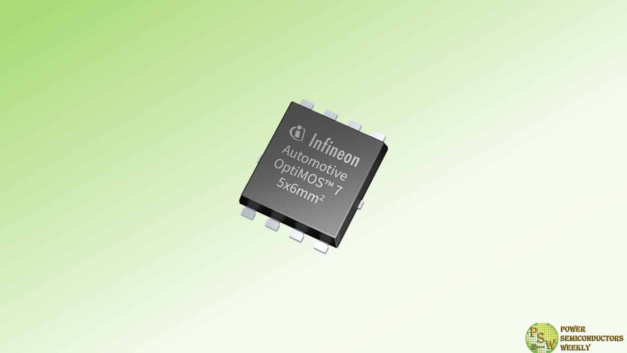
Infineon Technologies AG introduced the first product in its new advanced power MOSFET technology OptiMOS™ 7 80 V. The IAUCN08S7N013 features a significantly increased power density and is available in the versatile, robust, and high-current SSO8 5 x 6 mm² SMD package.
The OptiMOS™ 7 80 V offering is a perfect match for the upcoming 48 V board net applications. It is designed specifically for the high performance, high quality and robustness needed for demanding automotive applications like automotive DC-DC converters in EVs, 48 V motor control, for instance electric power steering (EPS), 48 V battery switches and electric two- and three-wheelers.
Compared to the previous generation, the R DS(on) of the Infineon IAUCN08S7N013 has been reduced by more than 50 percent, and is now the best R DS(on) in the industry with a maximum of 1.3 mΩ. Users benefit from minimized conduction losses, superior switching performance and the highest power density in a 5 x 6 mm² package.
In addition, the IAUCN08S7N013 also features low package resistance and inductance, as well as a high avalanche current capability. For automotive applications, it has an extended qualification that goes beyond AEC-Q101.
The IAUCN08S7N013 is in mass-production and available now. More information is available at www.infineon.com/iaucn08s7n013/.
Original – Infineon Technologies
