-
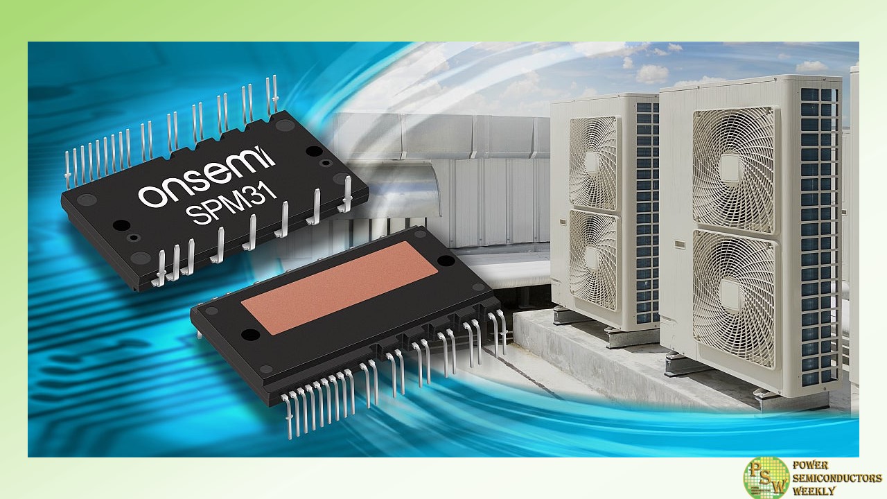
onsemi announced the availability of its 1200V SPM31 Intelligent Power Modules (IPMs) featuring the latest generation Field Stop 7 (FS7) Insulated Gate Bipolar Transistor (IGBT) technology. The SPM31 IPMs deliver higher efficiency, smaller footprint and higher power density resulting in lower total system cost than other leading solutions on the market.
Given the greater efficiency realized using optimized IGBTs, these IPMs are ideal for three-phase inverter drive applications such as heat pumps, commercial HVAC systems, servo motors, and industrial pumps and fans.
Operating residential and commercial buildings is estimated to contribute 26% of greenhouse gas emissions, with indirect emissions such as heating, cooling and powering buildings accounting for approximately 18%. As governments worldwide strive to meet their energy and climate commitments, more energy-efficient and lower-carbon solutions are becoming increasingly critical.
The SPM31 IPMs control the power flow to the inverter compressor and fans in heat pumps and air conditioning systems by adjusting the frequency and voltage of the power supplied to three-phase motors for maximum efficiency. For example, onsemi’s 25A-rated SPM31 using FS7 IGBT technology can decrease power losses by up to 10% and increase in power density up to 9%, compared to our previous generation products.
With the transition to electrification and heightened efficiency mandates, these modules help manufacturers drastically improve system design while increasing efficiency in heating and cooling applications. With the improved performance, our SPM31 IPM family featuring FS7 enables high efficiency with reduced energy losses, further reducing harmful emissions globally.
These highly integrated modules contain gate-driving ICs, multiple on-module protection features along with our FS7 IGBTs enabling industry-leading thermal performance with the ability to support a wide range of currents, from 15A to 35A. With their best-in-class power density, SPM31 FS7 IGBT IPMs are an ideal answer to save mounting space and improve performance expectations while shortening the development time. In addition, the SPM31 IPMs include the following benefits:
- Controls for gate drivers and protections
- Low loss, short-circuit-rated IGBTs
- Negative IGBT terminals available for each phase to support a wide variety of control algorithms
- Built-in under-voltage protection (UVP)
- Built-in bootstrap diodes and resistors
- Built-in high-speed high-voltage integrated circuit
- Single-grounded power supply
Original – onsemi
-
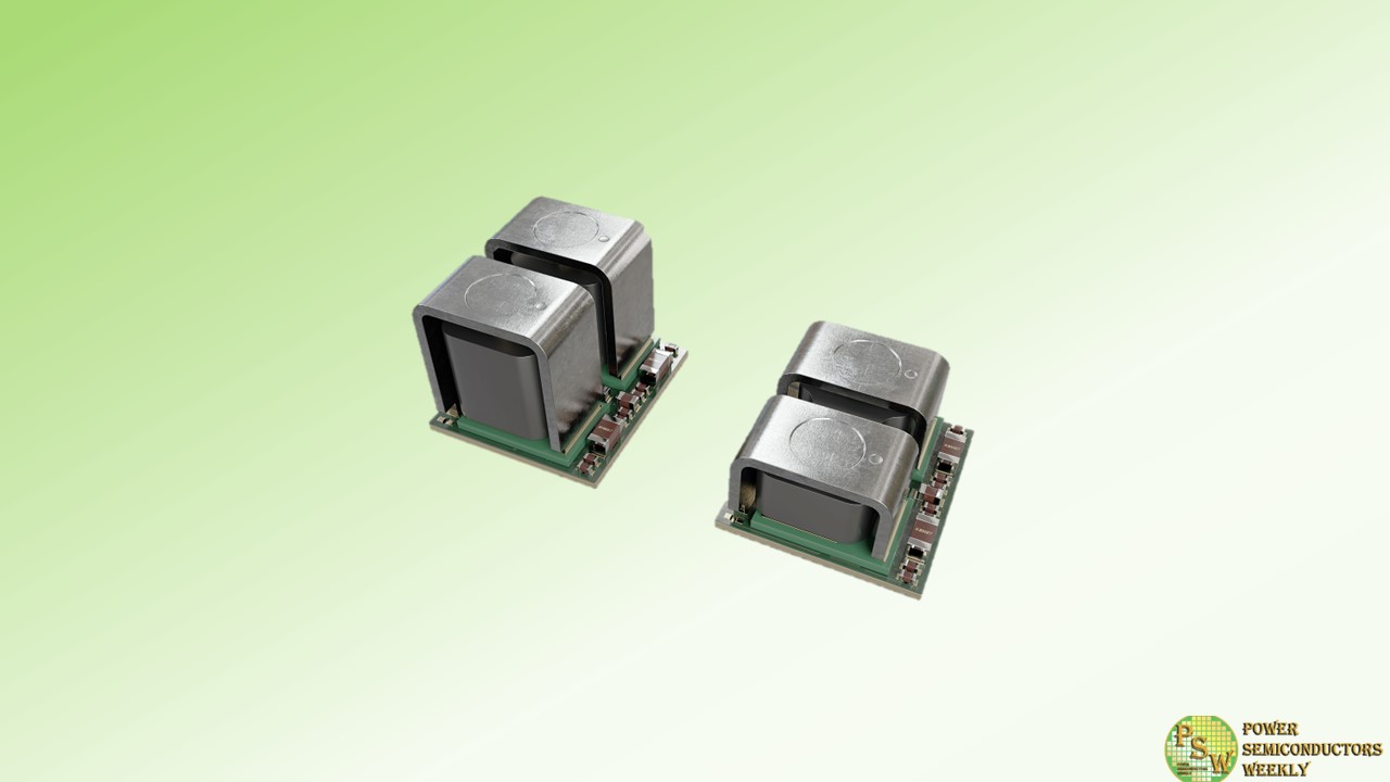
Artificial Intelligence is currently driving an exponential increase in global data generation, and consequently increasing the energy demands of the chips supporting this data growth. Infineon Technologies AG launched its TDM2254xD series dual-phase power modules that enable best-in-class power density, quality and total cost of ownership (TCO) for AI data centers.
The TDM2254xD series products blend innovation in robust OptiMOS TM MOSFET technology with novel packaging and proprietary magnetic structure to deliver industry-leading electrical and thermal performance with robust mechanical design. This lets data centers operate at higher efficiency to meet the high power demands of AI GPU (Graphic Processor Unit) platforms while also significantly reducing TCO.
Given that AI servers require 3 times more energy than traditional servers, and data centers already consume more than 2 percent of the global energy supply, it is essential to find innovative power solutions and architecture designs that further drive decarbonization. Paving the way for the green AI factory, Infineon’s TDM2254xD dual-phase power modules combine with XDP TM Controller technology to enable efficient voltage regulation for high-performance computing platforms with superior electrical, thermal and mechanical operation.
Infineon introduced the TDM2254xD series at the Applied Power Electronics Conference (APEC). The modules’ unique design allows for efficient heat transfer from the power stage on to the heat sink through novel inductor design that is optimized to transfer current and heat, thereby allowing for a 2 percent higher efficiency than industry average modules at full load. Improving power efficiency at the core of a GPU yields significant energy savings at scale. This translates into megawatts saved for data centers computing generative AI and in turn leads to reduced CO 2 emissions and millions of dollars in operating cost savings over the system’s lifetime.
“This unique Product-to-System solution combined with our cutting-edge manufacturing lets Infineon deliver solutions with differentiated performance and quality at scale, thereby significantly reducing total cost of ownership for our customers,” said Athar Zaidi, Senior Vice President, Power & Sensor Systems at Infineon Technologies. “We are excited to bring this solution to market; it will accelerate computing performance and will further drive our mission of digitalization and decarbonization.”
Original – Infineon Technologies
-

On 15 September 2023, the Management Board of Infineon Technologies AG resolved, with the approval of the Supervisory Board, to acquire up to 7,000,000 shares (ISIN DE0006231004) via the stock exchange at a total purchase price (excluding incidental costs) of up to €300 million.
The buyback is carried out on behalf of Infineon by an independent credit institution via Xetra trading on the Frankfurt Stock Exchange and is scheduled to start on 26 February 2024 and to be completed no later than 28 March 2024 (inclusive). The buyback serves the sole purpose of allocating shares to employees of the company or affiliated companies, members of the Management Board of the company as well as members of the management board and the board of directors of affiliated companies as part of the existing employee participation programs.
The buyback is based on the authorization granted by the Annual General Meeting on 16 February 2023 and will be carried out in accordance with Article 5 of Regulation (EU) 596/2014 in conjunction with the provisions of Commission Delegated Regulation (EU) No 2016/1052 of 8 March 2016 supplementing Regulation (EU) 596/2014 with regard to regulatory technical standards for the conditions applicable to buyback programs and stabilization measures (“Delegated Regulation (EU) 2016/1052”).
Further details can be found in the announcement pursuant to Art. 5(1) lit. a) of Regulation (EU) No 596/2014 and Art. 2(1) of Delegated Regulation (EU) 2016/1052 which has also been published on the Infineon website at www.infineon.com/cms/en/about-infineon/investor/infineon-share/. All transactions within the buyback program will be announced in accordance with the requirements of Delegated Regulation (EU) 2016/1052. Infineon will provide regular updates on the progress of the share buyback on its website at
https://www.infineon.com/cms/en/about-infineon/investor/infineon-share/#share-buyback-program-2024 and will ensure that the information remains publicly available for at least five years from the date of announcement.
Original – Infineon Technologies
-
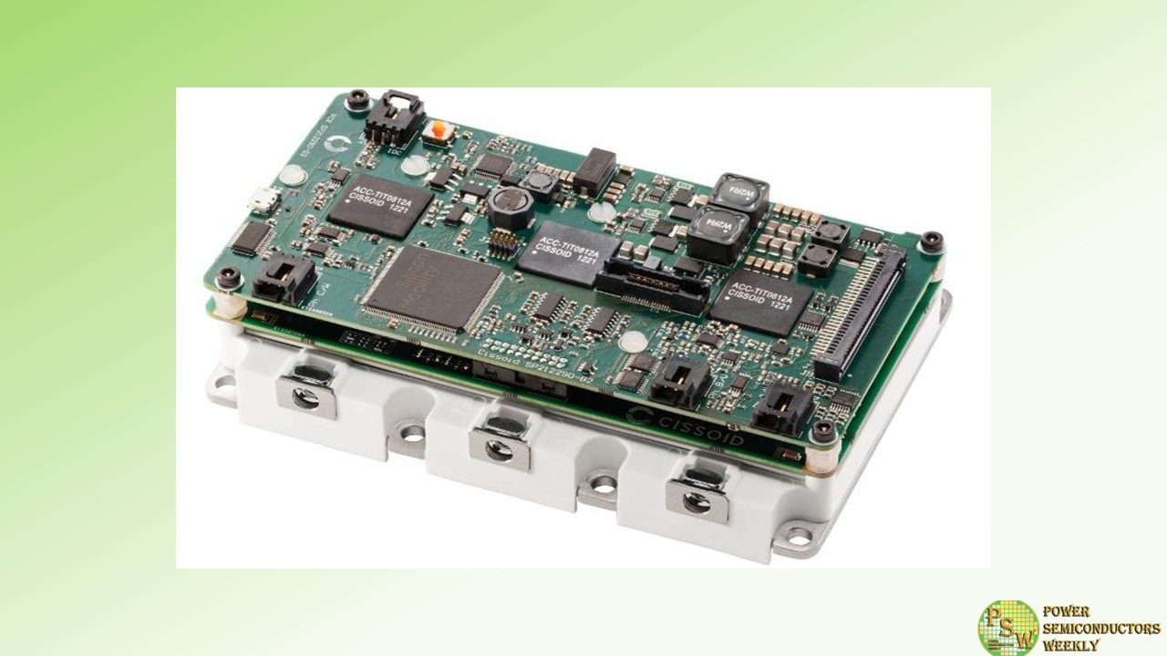
At the Applied Power Electronics Conference (APEC), CISSOID released its new series of SiC Inverter Control Modules (ICMs) dedicated to the E-mobility market. These software-powered SiC Inverter Control Modules are designed to help engineers create functionally safe, robust and modular E-motor drives while dramatically shortening time-to-market.
The new CXT-ICM3SA series offers optimal hardware and software integration of CISSOID’s existing line of 3-phase 1200V/340A-550A SiC MOSFET Intelligent Power Modules (IPMs) with an OLEA® T222 Field Programmable Control Unit (FPCU) control board and OLEA® APP INVERTER application software, supplied in partnership with Silicon Mobility. Depending on the selected ICM product, this modular core engine is capable of powering and controlling high voltage SiC traction inverters with battery voltages up to 850V, at output power exceeding 350kW, and with peak efficiency above 99%.
This unique integration facilitates the rapid development of SiC inverters by solving head-scratching EMC issues often generated due to fast-switching SiC transistors, by supporting different modulation schemes, e.g. SVPWM or DPWM, combined with dead time compensation, and by offering advanced motor control algorithms, including Field Oriented Control (FOC) and Flux Weakening management.
CISSOID further improves time-to-market by providing a complete SiC inverter reference design allowing motor bench testing of the ICM together with key peripheral elements such as current sensors, a high-performance DC-Link capacitor and EMI filter. Both the ICM and the reference design can be obtained from CISSOID, together with the motor control software and on-site technical support.Delivering leadership performance, the ICM supports the drive of high-speed motors, with no compromise on efficiency, thanks to the combination of CISSOID’s low losses SiC power module with the ultra-fast real-time FPCU, enabling high switching frequencies up to 50kHz. Furthermore, this application-specific processor dedicated to e-motor control, with onboard programmable hardware, accelerates the response time to critical events, off-loading the processor cores and enhancing functional safety. Both the FPCU and the control software are ISO-26262 ASIL C/D certified and AUTOSAR 4.3 compliant.
Original – CISSOID
-
Bourns, Inc. announced it has selected Holder as an additional full line distributor in China. Holder was selected based on its extensive passive components experience along with its knowledgeable and large FAE organization that is known to supply superior technical support. These attributes give Bourns the essential backing to meet increasing demand for the company’s advanced vehicle, industrial and consumer electronic component solutions.
“As the leading passive component distributor in China, it made strategic sense for Bourns to initiate a sales channel relationship with Holder. Bourns has grown to be one of the Top 10 power conversion solution providers worldwide. Therefore, we believe this strategic alliance is poised to bring about a positive impact on meeting our customers’ growing need for Bourns’ product accessibility and availability in the Chinese market,” said James Harrington and Senior Vice President of Worldwide Sales at Bourns.
“The entire Holder organization is excited to take on the representation of Bourns’ advanced and innovative application solutions. With 29 offices throughout China along with an extensive FAE team, we are eager to help Bourns expand its Chinese customer base with the worldclass support electronics developers have come to expect from an industry leader such as Bourns,” said Leo Xie, Holder CEO.
Original – Bourns
-

Infineon Technologies AG has finished its 24th Annual General Meeting. The entire event was held in a virtual format and broadcast publicly on the company web site. Shareholders had the opportunity to speak live during the event and ask questions.
Dividend of €0.35 per share
The Annual General Meeting followed the proposal of the Management Board and Supervisory Board on the distribution of profits and approved a dividend payment of €0.35 per share. The payout exceeds the dividend amount of the previous year by 3 Euro cents, or almost 10 percent.
Ute Wolf and Prof. Dr. Hermann Eul elected to the Supervisory Board
Ute Wolf was appointed to the Supervisory Board by court order from 22 April 2023 until the end of the 2024 Annual General Meeting. Her term of office as a shareholder representative on the Supervisory Board was extended by the Annual General Meeting. In addition, Dr. Manfred Puffer resigned from his position with effect from the end of the Annual General Meeting on 23 February 2024, meaning that his vacant position had to be filled. The Annual General Meeting elected Prof. Dr. Hermann Eul as a new member of the Supervisory Board.
Deloitte elected as new corporate auditor
The shareholders elected Deloitte GmbH, Munich, as auditor for the 2024 financial year. The tender process had been carried out as part of the legally required rotation.
Detailed information on the 2024 Infineon Technologies AG Annual General Meeting, including the voting results for the individual agenda items, is available at www.infineon.com/agm, together with the recorded speeches of the Chairman of the Supervisory Board, the Chief Executive Officer and the Chief Financial Officer.
Original – Infineon Technologies
-
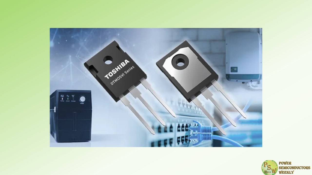
Toshiba Electronic Devices & Storage Corporation has added DTMOSVI(HSD), power MOSFETs with high-speed diodes suitable for switching power supplies, including data centers and photovoltaic power conditioners, to its latest-generation DTMOSVI series with a super junction structure. Shipments of the first two products “TK042N65Z5” and “TK095N65Z5,” 650V N-channel power MOSFETs in TO-247 packages, start today.
The new products use high-speed diodes to improve the reverse recovery characteristics important for bridge circuit and inverter circuit applications. Against the standard DTMOSVI, they achieve a 65% reduction in reverse recovery time (trr), and an 88% reduction in reverse recovery charge (Qrr) (measurement conditions: -dIDR/dt= 100A/μs).
The DTMOSVI(HSD) process used in the new products improves on the reverse recovery characteristics of Toshiba’s DTMOSIV series with high-speed diodes (DTMOSIV(HSD)), and has a lower drain cut-off current at high temperatures. The figure of merit “drain-source On-resistance × gate-drain charges” is also lower. The high temperature drain cut-off current of TK042N65Z5 is approximately 90% lower, and the drain-source On-resistance × gate-drain charge 72% lower, than in Toshiba’s current TK62N60W5.
This advance will cut equipment power loss and help to improve efficiency. The TK042N65Z5 shows a maximum improvement in power supply efficiency over the current TK62N60W5 of about 0.4%, as measured in a 1.5kW LLC circuit.
A reference design, “1.6 kW Server Power Supply (Upgraded)”, that uses TK095N65Z5 is available on Toshiba’s website today. The company also offers tools that support circuit design for switching power supplies. Alongside the G0 SPICE model, which verifies circuit function in a short time, highly accurate G2 SPICE models that accurately reproduce transient characteristics are now available.
Toshiba plans to expand the DTMOSVI(HSD) line-up with the release of devices in TO-220 and TO-220SIS through-hole packages, and TOLL and DFN 8×8 surface-mount packages.
The company also will continue to expand its line-up of the DTMOSVI series beyond the already released 650V and 600V products and the new products with high-speed diodes. This will enhance switching power supply efficiency, contributing to energy-saving equipment.
Original – Toshiba
-
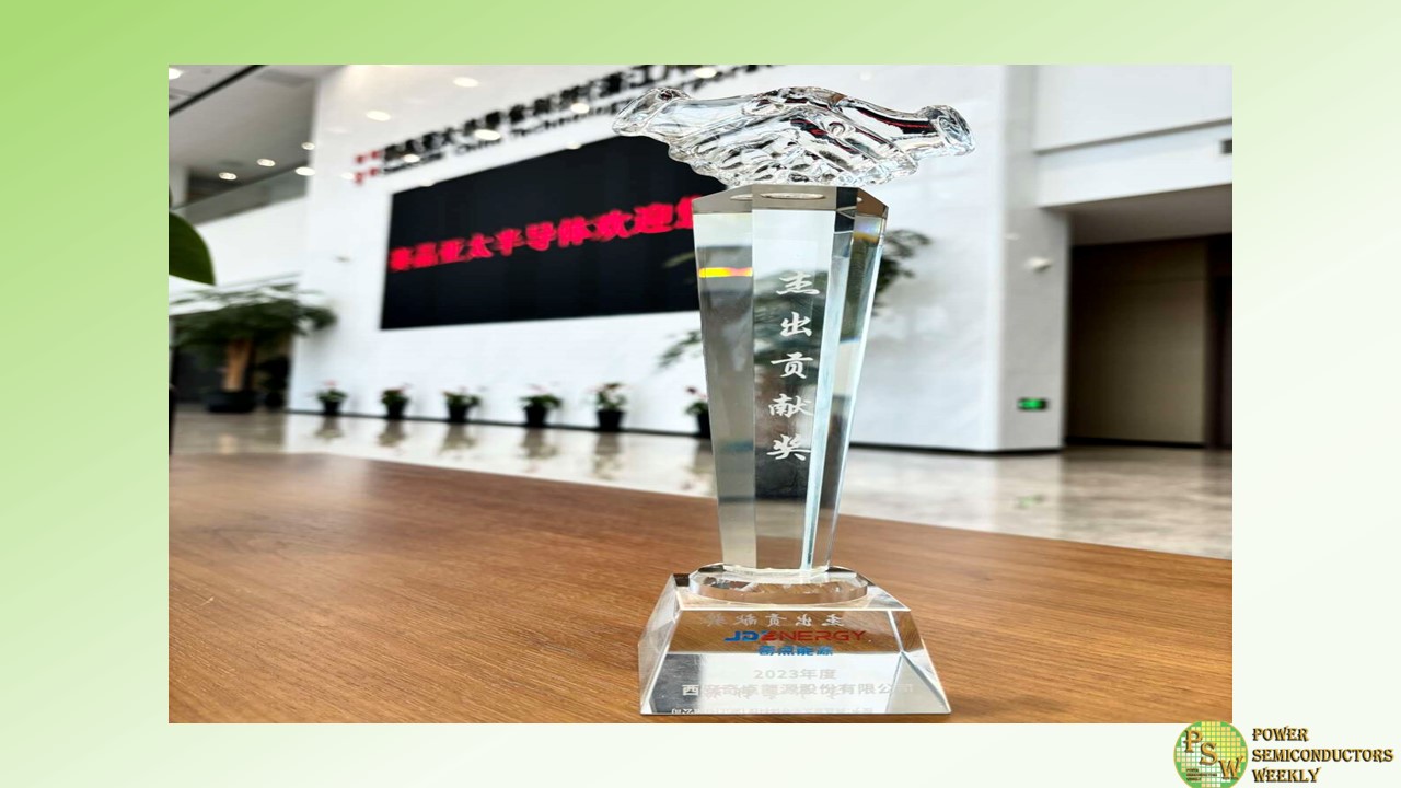
SwissSEM received JD Energy 2023 Outstanding Contribution Award. The Outstanding Contribution Award harvested in 2023 is not only JD Energy’s affirmation of SwissSEM’s product performance and service quality, but also demonstrates its confidence in SwissSEM’s future development. SwissSEM will continue to strengthen exchanges and cooperation with customers, and strive to the international first-class level of domestic boutique power semiconductors, to help China’s new energy industry take off.
JD Energy is a company founded in 2018, relying on Xi’an Jiaotong University, jointly founded by industry-renowned power electronics technology experts and a group of senior engineers with more than 10 years of development experience. JD Energy is committed to technical research and product development of core equipment in advanced energy storage systems, contributing industry-leading solutions to promote large-scale clean energy access and achieve global carbon neutrality goals, which is a key partner of SwissSEM.
Since 2022, SwissSEM has been a supplier to JD Energy, supplying 1200V ED-type modules to it in bulk for use in the energy storage converter, and has achieved a high product share in 2023. According to JD Energy’s feedback, SwissSEM’s module products are of excellent quality, with outstanding consistency and reliability, thoughtful after-sales technical support services, quick response time, and are trustworthy and excellent suppliers.
The Outstanding Contribution Award harvested in 2023 is not only JD Energy’s affirmation of SwissSEM’s product performance and service quality, but also demonstrates its confidence in SwissSEM’s future development. SwissSEM will continue to strengthen exchanges and cooperation with customers, and strive to the international first-class level of domestic boutique power semiconductors, to help China’s new energy industry take off.
Original – SwissSEM
-

Infineon Technologies AG and ASE Technology Holding Co., Ltd. announced that definitive agreements were signed under which Infineon will sell two backend manufacturing sites, one in Cavite, Philippines and one in Cheonan, South Korea, to two fully owned subsidiaries of ASE, a leading provider of independent semiconductor manufacturing services in assembly and test.
The plants currently run under the entity names Infineon Technologies Manufacturing Ltd. – Philippine Branch (Cavite) and Infineon Technologies Power Semitech Co., Ltd. (Cheonan) and will be acquired by ASE Inc. and ASE Korea Inc. respectively. Post the transaction, ASE will assume operations with current employees, and further develop both sites to support multiple customers. As such, ASE and Infineon have also concluded long-term supply agreements under which Infineon will continue to receive previously established services as well as services for new products to support its customers and fulfill existing commitments.
Infineon’s manufacturing strategy, with a balanced operations footprint combining in-house and external manufacturing, is an important pillar of the company’s profitable growth path. By pooling manufacturing volumes in Cavite and Cheonan under a new owner and offering highest-quality manufacturing services to the overall industry, Infineon and ASE will be able to leverage mutual synergy potentials, thus generating attractive growth potentials for both companies.
“We have excellent, highly competent teams and a great track record of highest quality standards at both sites, Cavite and Cheonan,” said Alexander Gorski, EVP and Head of Backend Operations at Infineon. “ASE has been a trusted, strategic partner of Infineon for many years and will be an excellent new owner that will continue on this successful path and strengthen both fabs even further. The sale of our sites to ASE is in line with Infineon’s manufacturing strategy, provides mutual synergies and enables further growth while strengthening supply chain resilience”.
“Both the automotive and power management market segments are strategic focus areas for ASE,“ said Dr. Tien Wu, Chief Operating Officer of ASE. “This acquisition of Infineon’s facilities in Cavite and Cheonan marks ASE’s strong commitment to form a strategic long-term partnership with Infineon in developing backend manufacturing solutions matching future growth opportunities. Given Infineon’s market leadership in automotive and power semiconductors and ASE’s leading position in backend semiconductor manufacturing, this partnership creates a win-win solution for the entire ecosystem from product companies to the end consumer.”
Infineon Technologies Power Semitech is a backend manufacturing site with around 300 employees. The fab is located in Cheonan, South Korea, about 60 miles south of Seoul. Infineon Technologies Cavite, is a backend manufacturing site with more than 900 employees. It is located in one of the fastest growing and most industrialized provinces in the Philippines.
The transaction is expected to close towards the end of the second calendar quarter of 2024, when all pending closing conditions will have been fulfilled.
Original – Infineon Technologies
-
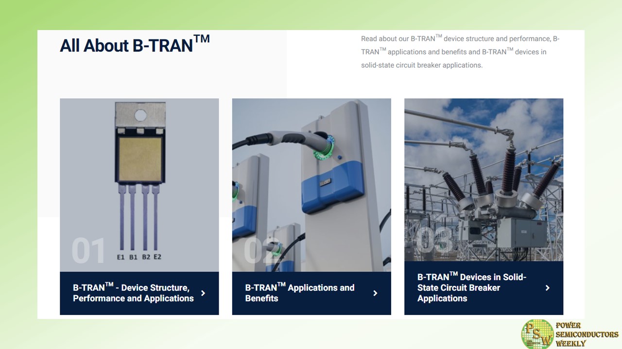
Ideal Power Inc. announced the successful completion of Phase II deliverables of a product development agreement with Stellantis, a top 10 global automaker.
Ideal Power is partnering with Stellantis’ advanced technology development team to develop a custom B-TRAN™ power module for use in electric vehicle (“EV”) drivetrain inverters in Stellantis’ next generation EV platform. Due to its compelling advantages, B-TRAN™ is also being evaluated for the automaker’s vehicle power management and EV charging ecosystem.
All Phase I deliverables were successfully completed including a wafer run and delivery of packaged and tested B-TRAN™ devices and test boards to both Stellantis and the program’s packaging company. Ideal Power also provided technical support, device characterization and test data to Stellantis on B-TRAN™ performance and related drive circuitry. The B-TRAN™ devices delivered to Stellantis outperformed the device performance specifications provided to Stellantis at the beginning of the program.
All Phase II deliverables were successfully completed ahead of schedule including a wafer run and delivery of tested B-TRAN™ devices and drivers to both the program’s packaging company and the organization building the initial drivetrain inverter. In Phase II, Ideal Power collaborated closely with Stellantis and the program partners to supply B-TRAN™ devices for integration into the custom power module and inverter designs.
The device testing results by the Stellantis program team validated the expected efficiency improvements anticipated from B-TRAN™ use in the drivetrain and its readiness for implementation in EV applications. Stellantis also approved the comprehensive reliability test plan for automotive qualification provided by Ideal Power.
Phase III builds on the completion of all Phase I and II deliverables and therefore transitions to Stellantis’ production team. Ideal Power and Stellantis are currently finalizing the scope of work for the next phase of the program. This phase is expected to include the extensive testing of the custom B-TRAN™ module to meet automotive certification standards enabling B-TRAN™ to be the core of the powertrain inverter for the automaker’s next-generation EVs. The objective of this phase is the completion and certification of a production-ready B-TRAN™-based module and is targeted for 2025.
“We’re thrilled with the success of both Phase I and II and advancement into the next phase of the program with Stellantis. Successful completion of Phases I and II were customer validation of the performance of B-TRAN™ and its potential impact in improving EV range and cost,” said Dan Brdar, President and Chief Executive Officer of Ideal Power. “We are leveraging our success with Stellantis to attract and engage other automobile OEMs and Tier 1 auto suppliers.”
This program represents Ideal Power’s second engagement with the world’s leading automotive manufacturers as another top 10 global automaker is already in company’s test and evaluation program.
Original – Ideal Power
