
-
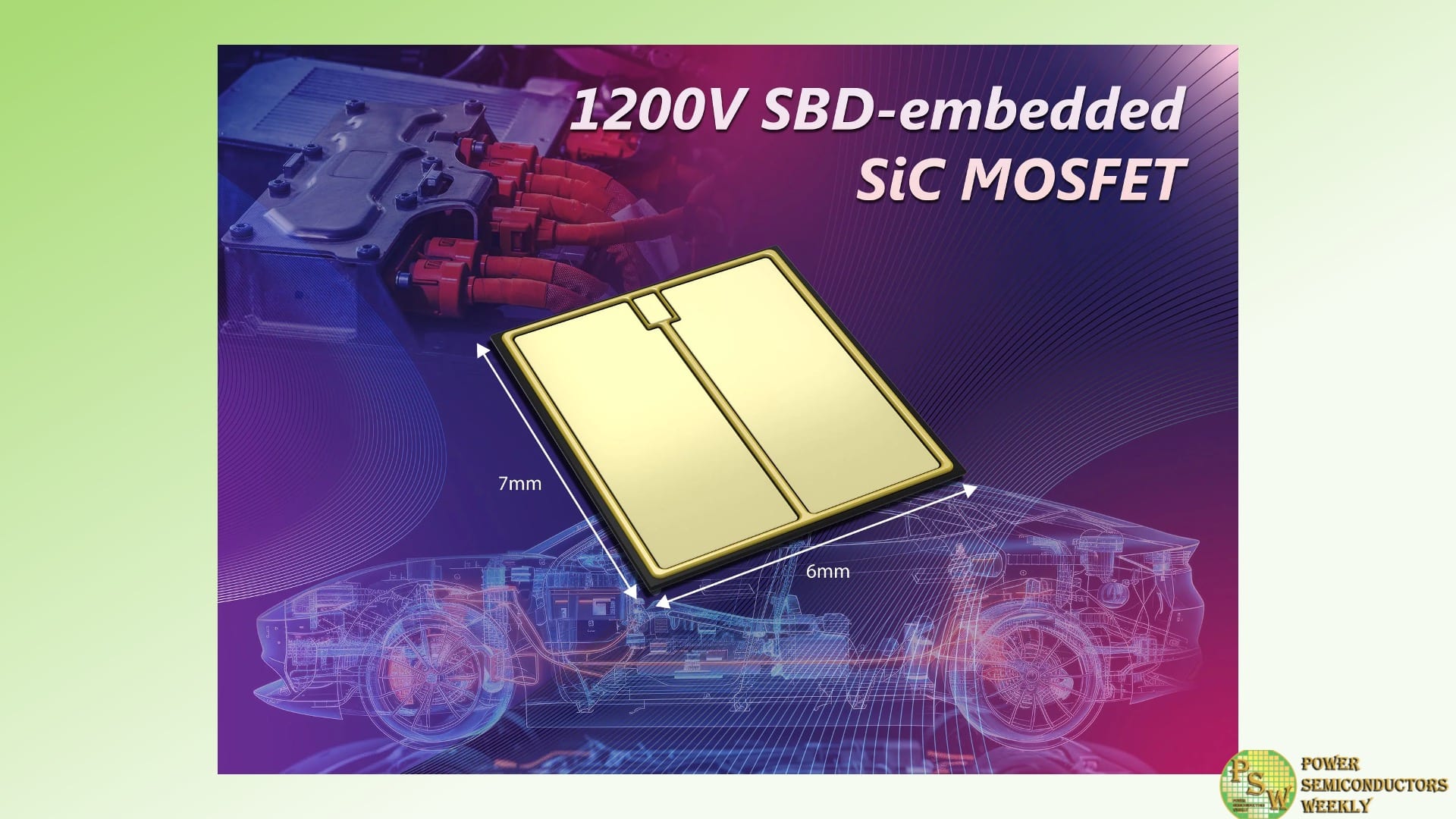
Toshiba Electronics Europe GmbH has developed new 1200V silicon carbide (SiC) MOSFETs with low on-resistance (RDS(ON)) and high levels of reliability. The devices are particularly suited to applications within automotive traction inverters. They are now available and shipping as early test samples in bare die format – allowing customers to customise them to meet the needs of their applications.
The new X5M007E120 uses a manufacturing process that reduces on-resistance per unit area by up to 30%. Unlike existing methods that utilise a striped-pattern construction, the new devices arrange the embedded Schottky barrier diodes (SBDs) in a check-pattern to achieve lower on-resistance.
Many SiC MOSFETs increase on-resistance as body diodes are energised during reverse conduction, which can lead to reliability issues. Toshiba SiC MOSFETs alleviate this issue by preventing body diodes from operating as SBDs are embedded into the MOSFETs. This approach maintains the reduction in on-resistance while ensuring reliability during reverse conduction.
With electric motors consuming over 40% of the world’s electrical energy, efficient operation is essential to sustainability. The re-arrangement of SBDs in this device has suppressed body diode energisation, and the upper limit of unipolar operation has increased to around double without increasing the SBD mounting area. Additionally, channel density is improved. These enhancements contribute to energy efficiency in applications, including motor control inverters.
Reducing RDS(ON) within a SiC MOSFET can cause excess current flow during short-circuit operations. By adopting a deep barrier structure, the X5M007E120 reduces excessive current within the MOSFET section and leakage current in the SBDs section during short-circuit operation. This enables durability during short-circuit conditions while maintaining high levels of reliability against reverse conduction operation.
The new X5M007E120 has a VDSS of 1200V and is rated for a drain current (ID) of 229A continuously, with 458A for pulsed operation (ID Pulse). RDS(ON) is as low as 7.2mΩ, and the device can operate with channel temperatures (Tch) as high as 175°C. The devices are AEC-Q100 qualified for automotive applications.
Engineering samples of the new X5M007E120 are expected to ship during 2025, with mass production samples scheduled to start in 2026.
Toshiba will continue to seek ways to further improve the characteristics of its products. The company will contribute to realising a decarbonised society by providing customers with power semiconductors for applications where energy efficiency is essential, such as inverters for motor control and power control systems for electrical vehicles.
Original – Toshiba
-
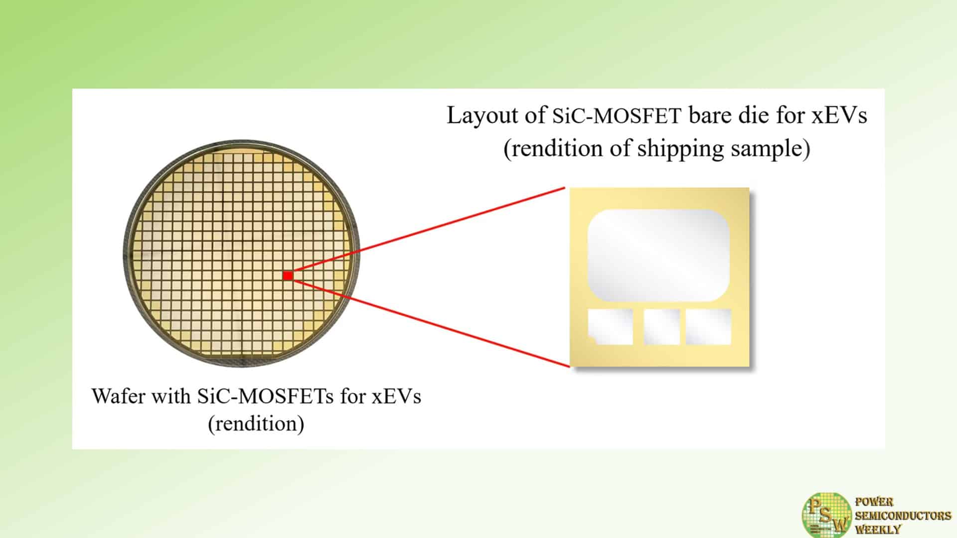
Mitsubishi Electric Corporation announced that it will begin shipping samples of a silicon carbide (SiC) metal-oxide-semiconductor field-effect transistor (MOSFET) bare die for use in drive-motor inverters of electric vehicles (EVs), plug-in hybrid vehicles (PHEVs) and other electric vehicles (xEVs) on November 14.
Mitsubishi Electric’s first standard-specification SiC-MOSFET power semiconductor chip will enable the company to respond to the diversification of inverters for xEVs and contribute to the growing popularity of these vehicles. The new SiC-MOSFET bare die for xEVs combines a proprietary chip structure and manufacturing technologies to contribute to decarbonization by enhancing inverter performance, extending driving range and improving energy efficiency in xEVs.
Mitsubishi Electric’s new power semiconductor chip is a proprietary trench SiC-MOSFET that reduces power loss by about 50% compared to conventional planar SiC-MOSFETs. Thanks to proprietary manufacturing technologies, such as a gate oxide film process that suppresses fluctuations in power loss and on-resistance, the new chip achieves long-term stability to contribute to inverter durability and xEV performance.
Original – Mitsubishi Electric
-
Littelfuse, Inc. announced the release of the IXTN400N20X4 and IXTN500N20X4 Ultra Junction X4-Class Power MOSFETs.
The new devices expand upon the current 200 V X4-Class Ultra Junction MOSFETs, featuring some of the lowest on-state resistances available. The high current ratings of these MOSFETs allow designers to replace multiple low-current rated devices connected in parallel, streamlining the design process and enhancing both reliability and power density in applications. Additionally, the screw-mounted terminals of the SOT-227B package enable rugged and stable mounting.
These new 200 V MOSFETs deliver the lowest on-state resistances, enhancing and complementing the existing Littelfuse X4-Class Ultra Junction family portfolio. Compared to the existing state-of-the-art X4-Class MOSFET solutions, these MOSFETs offer up to ~2x higher current ratings and RDS(on) values up to ~63% lower.
The new MOSFETs are ideal for a range of low-voltage power applications where minimizing on-state losses is essential, including:
- Battery Energy Storage Systems (BESS),
- Battery chargers,
- Battery formation,
- DC/battery load switch, and
- Power supplies.
“The new devices will allow designers to replace multiple low-current rated devices, connected in parallel, with a single device solution,” said Sachin Shridhar Paradkar, Global Product Marketing Engineer at Littelfuse. “This unique solution simplifies gate driver design, improves reliability, improves power density and PCB space utilization.”
The Ultra Junction X4-Class Power MOSFET offers the following key performance benefits:
- Low conduction losses
- Minimized parallel connection effort
- Simplified driver design with minimal driver losses
- Simplified thermal design
- Increased power density
A MOSFET with low on-state resistance (RDS(on)) is the ideal choice in applications where minimal on-state losses are crucial. It significantly reduces the power dissipation during operation, leading to lower conduction losses, higher efficiency, and less heat generation. This makes it perfect for power-sensitive applications such as power supplies, motor drivers, and battery-operated devices where maintaining high efficiency and thermal management is crucial.
Performance Specifications
Performance Specs IXTN500N20X4 IXTN400N20X4 Package Aluminum-nitride ceramic-based isolated SOT-227B On-state resistance RDS(on) = 1.99 mΩ @ Tvj = 25°C RDS(on) = 3 mΩ @ Tvj = 25°C High nominal current rating 500 A @ TC = 25°C 340 A @ TC = 25°C Gate charge Qg = 535 nC Qg = 348 nC Thermal resistance RthJC = 0.13 K/W RthJC = 0.18 K/W Original – Littelfuse
-

Nexperia introduced a new series of high-performance gate driver ICs designed for driving both high-side and low-side N-channel MOSFETs in a synchronous buck or half-bridge configuration. These devices deliver high current output and excellent dynamic performance, boosting efficiency and robustness in applications.
The automotive-qualified NGD4300-Q100 is ideal for electronic power steering and power converters, while the NGD4300 has been designed for use with DC-DC converters in consumer devices, servers and telecommunications equipment as well as for micro-inverters used in various industrial applications.
The floating high-side driver in these ICs can operate from bus voltages up to 120 V and use a bootstrap supply with an integrated diode, features which simplify overall system design and help to reduce PCB size. They can deliver up to 4 A (peak) source and 5 A of sink current to guarantee short rise and fall times even for heavy loads.
The gate driver has a low 13 ns delay and offers excellent channel-to-channel delay matching of only 1 ns. These delays are significantly lower than for similar competing gate drivers and help to minimize dead-time by maximizing switching duty-cycle. 4 ns rise and 3.5 ns (typical) fall times help to deliver higher efficiency and support high frequency and fast system control. These gate drivers accept input control signals complying with both TTL and CMOS logic levels.
“These devices are the first in our new portfolio of high-performance half-bridge gate drivers” according to Irene Deng, general manager of the IC solutions business group at Nexperia. “This release demonstrates how Nexperia is using process innovation to respond to the burgeoning demand for robust gate drivers that can increase power converter efficiency while also delivering smoother motor control in consumer, industrial and automotive applications.”
For superior robustness in power conversion and motor driving applications, these ICs are fabricated using a silicon-on-insulator (SOI) process. This allows the negative voltage tolerance of the HS pin to extend to -5 V, significantly reducing the risk of damage caused by system parasitic component and unexpected spikes. The NGD4300 and NGD4300-Q100 are available in a choice of DFN-8, SO-8 and HSO-8 packages to offer engineers the flexibility to trade-off between device size and thermal performance, depending on application requirements.
Original – Nexperia
-
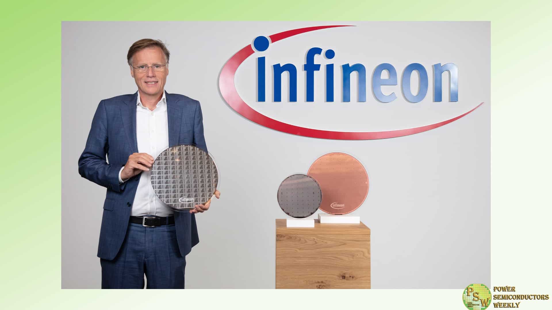
Infineon Technologies AG is reporting results for the fourth quarter and the full fiscal year, both of which ended on 30 September 2024.
“Infineon has managed the 2024 fiscal year well and concluded it in line with expectations,” says Jochen Hanebeck, CEO of Infineon. “Currently, there is hardly any growth momentum in our end markets except from AI, the cyclical recovery is being delayed. The inventory correction is continuing. Short-term ordering patterns and inventory digestion are clouding visibility on demand trends beyond the next couple of quarters. We are therefore preparing for a muted business trajectory in 2025. At the same time, we are relying on the consistent implementation of the structural measures in our “Step Up” program to strengthen our competitiveness. In combination with our innovative power, we are addressing our structural growth drivers and putting ourselves in the best position for a coming upturn.”
- Q4 FY 2024: Revenue €3.919 billion, Segment Result €832 million, Segment Result Margin 21.2 percent
- FY 2024: Revenue €14.955 billion, down 8 percent on the prior year; Segment Result €3.105 billion; Segment Result Margin 20.8 percent; adjusted earnings per share €1.87; Free Cash Flow €23 million, adjusted Free Cash Flow €1.690 billion
- Dividend proposal for FY 2024: Dividend unchanged at €0.35 per share
- Outlook for Q1 FY 2025: Based on an assumed exchange rate of US$1.10 to the euro, revenue of around €3.2 billion expected. On this basis, Segment Result Margin forecast to be in the mid-teens percentage range
- Outlook for FY 2025: Based on an assumed exchange rate of US$1.10 to the euro, revenue is expected to slightly decline compared with previous year. The adjusted gross margin should be around 40 percent and the Segment Result Margin in the mid-to-high-teens percentage range. Investments of approximately €2.5 billion planned. Free Cash Flow adjusted for investments in frontend buildings should be around €1.7 billion and reported Free Cash Flow around €900 million
For the full version of this news release (incl. financial data), please download the PDF version.
Original – Infineon Technologies
-

Cambridge GaN Devices (CGD) and IFP Energies nouvelles (IFPEN), a major French public research and training organization in the fields of energy, transport and the environment, have developed a demo which confirms the suitability of CGD’s ICeGaN®650 V GaN ICs in a multi-level, 800 VDC inverter.
The demo delivers super-high power density – 30 kW/l – which is greater than can be achieved by more expensive, state-of-the-art silicon-carbide (SiC)-based devices. The inverter realization also demonstrates the ease of paralleling that ICeGaN technology enables; each inverter node has three 25mΩ / 650V ICeGaN ICs – 36 devices in total – in parallel.
ANDREA BRICCONI | CHIEF MARKETING OFFICER, CGD
“We are super excited at this first result of our partnership with IFPEN. 800 VDC supports the 800 V bus which is being increasingly adopted by the EV industry. By addressing automotive and other high voltage inverter applications with energy-efficient ICeGaN-based solutions we are delivering on CGD’s key commitment – sustainability.”This multi-level GaN Inverters can power electric motors to over 100 kW peak, 75 kW continuous power. The CGD/IFPEN demo features: a high voltage input of up to 800Vdc; 3-phase output; a peak current of 125 Arms (10s) (180 Apk); and a continuous current of 85 Arms continuous (120 Apk).
The ICeGaN multi-level design proposed by IFPEN reveals several compelling benefits:
- Increased Efficiency: the improvement in the efficiency of the traction inverter leads to an increase in battery range and a reduction in charging cycles. It also leads to a reduction in battery cost if the initial range (iso-range) is maintained
- Higher switching frequencies: GaN transistors can operate at much higher frequencies than silicon transistors. This reduces iron losses in the motor, particularly in the case of machines with low inductances
- Reduced Electromagnetic Interferences: 3-level topology minimizes EMI and enhances the reliability of the system
- Enhanced thermal management: insulated metallized substrate boards featuring an aluminium core facilitate superior thermal dissipation, ensuring optimal operating temperatures and extending the lifespan of the system and associated GaN devices
- Modular design: this facilitates scalability and adaptability for varying system requirements.
GAETANO DE PAOLA | PROGRAM MANAGER, IFPEN
“Following the implementation of this inverter reference using CGD’s enabling ICeGaN ICs coupled with innovative topologies, such as multi-level solutions, IFPEN now strongly believes that GaN is a breakthrough technology in terms of performance and cost for high-voltage traction inverters.”Original – Cambridge GaN Devices
-

ROHM has developed surface mount SiC Schottky barrier diodes (SBDs) that improve insulation resistance by increasing the creepage distance between terminals. The initial lineup includes eight models – SCS2xxxNHR – for automotive applications such as onboard chargers (OBCs), with plans to deploy eight models – SCS2xxxN – for industrial equipment such as FA devices and PV inverters in December 2024.
The rapidly expanding xEV market is driving the demand for power semiconductors, among them SiC SBDs, that provide low heat generation along with high-speed switching and high-voltage capabilities in applications such as onboard chargers. Additionally, manufacturers increasingly rely on compact surface mount devices (SMDs) compatible with automated assembly equipment to boost manufacturing efficiency. Compact SMDs tend to typically feature smaller creepage distances, fact that makes high-voltage tracking prevention a critical design challenge.
As leading SiC supplier, ROHM has been working to develop high-performance SiC SBDs that offer breakdown voltages suitable for high-voltage applications with ease of mounting. Adopting an optimized package shape, it achieves a minimum creepage distance of 5.1mm, improving insulation performance when contrasted with standard products.
The new products utilize an original design that removes the center pin previously located at the bottom of the package, extending the creepage distance to a minimum of 5.1mm, approx. 1.3 times greater than standard products. This minimizes the possibility of tracking (creepage discharge) between terminals, eliminating the need for insulation treatment through resin potting when surface mounting the device on circuit boards in high voltage applications. Additionally, the devices can be mounted on the same land pattern as standard and conventional TO-263 package products, allowing an easy replacement on existing circuit boards.
Two voltage ratings are offered, 650V and 1200V, supporting 400V systems commonly used in xEVs as well as higher voltage systems expected to gain wider adoption in the future. The automotive-grade SCS2xxxNHR are AEC-Q101 qualified, ensuring they meet the high reliability standards this application sector demands.
Going forward, ROHM will continue to develop high-voltage SBDs using SiC, contributing to low energy consumption and high efficiency requirements in automotive and industrial equipment by providing optimal power devices that meet market needs.
Original – ROHM
-

Texas Instruments (TI) announced the opening of its new, state-of-the-art product distribution center in Dreieich, Germany, outside of Frankfurt. This new distribution center includes 9,000 square meters of space and new automation features. The new center has the capacity to quickly ship up to 7,500 orders per day of a broad range of TI analog and embedded processing semiconductors across Europe.
“Our new product distribution center offers faster, more efficient, flexible and reliable service for TI’s customers in Europe to meet semiconductor demand now and in the future,” said Stefan Bruder, president of Texas Instruments Europe. “Our new center in Dreieich is the latest addition to TI’s global product distribution network which, combined with our convenient purchasing options, provides an improved customer experience from product selection to shipment.”
Located near many of TI’s industrial and automotive customers, as well as the Frankfurt Airport, the new distribution center enables faster product delivery in Europe. The pick, pack and ship process is fully automated and orders are ready to ship within 15 minutes or less. Customers in central Germany can expect same-day product delivery, while next-day delivery is available to customers in most European countries.
TI has been operating in Europe since 1956, and its new distribution center builds on TI’s existing European footprint which includes a semiconductor wafer factory in Freising, Germany, research and development teams, as well as more than 30 sales offices across 18 different European countries.
Customers in Europe and across the globe can conveniently buy from TI and save on exchange fees with more than 20 currency options available (including euro, pound sterling, Norwegian kroner and Swiss franc) when purchasing on TI.com or through TI API suites.
Original – Texas Instruments
-

Qorvo® announced the election of Mr. Alan S. Lowe to its Board of Directors, effective November 11, 2024. Mr. Lowe also joined the Board’s Audit Committee.
Since 2015, Mr. Lowe has served as president and chief executive officer of Lumentum Holdings Inc., a designer and manufacturer of optical and photonic products enabling optical networking and laser applications worldwide.
Prior to Lumentum’s separation from Viavi Solutions Inc. in 2015, Mr. Lowe was employed by Viavi. Mr. Lowe joined Viavi in September 2007 as senior vice president of the Lasers business and became executive vice president and president of Viavi’s communications and commercial optical products business in October 2008.
Bob Bruggeworth, President and Chief Executive Officer of Qorvo, said, “I am delighted that Alan is joining our Board of Directors. He brings terrific experience, insight and leadership to our Board, and we look forward to his contributions.”
“Qorvo is recognized globally for its product and technology leadership,” said Mr. Lowe. “I am excited to join Qorvo’s Board, and I look forward to working with my fellow directors in continuing Qorvo’s growth and creating long-term value for its shareholders.”
Original – Qorvo
-

Power components are evolving to meet the increasing demands for higher efficiency, smaller size and greater performance in power electronic systems. To provide system designers with a wide range of power solutions, Microchip Technology announced its portfolio of IGBT 7 devices offered in different packages, multiple topologies, and current and voltage ranges.
Featuring increased power capability, lower power losses and compact device sizes, this new portfolio is designed to meet high-growth market segments such as sustainability, E-Mobility and data centers. These high-performance IGBT 7 devices are key building blocks for power applications in solar inverters, hydrogen ecosystems, commercial and agricultural vehicles and More Electric Aircraft (MEA).
Designers can select a suitable power solution based on their requirements. The IGBT 7 devices are offered in standard D3 and D4 62 mm packages, as well as SP6C, SP1F and SP6LI packages. Many configurations are available in the following topologies: three-level Neutral-Point Clamped (NPC), three-phase bridge, boost chopper, buck chopper, dual-common source, full-bridge, phase leg, single switch and T-type. Devices are available with voltages ranging from 1200V to 1700V and current ranging from 50A to 900A.
“The versatile IGBT 7 portfolio combines ease of use and cost efficiency with higher power density and reliability, offering our customers maximum flexibility. These products are designed for general industrial applications as well as specialized aerospace and defense applications,” said Leon Gross, corporate vice president of Microchip’s discrete product group. “Additionally, our power solutions can be integrated with Microchip’s broad range of FPGAs, microcontrollers (MCUs), microprocessors (MPUs), dsPiC® Digital Signal Controllers (DSCs) and analog devices to provide a comprehensive system solution from one supplier.”
The lower on-state IGBT voltage (Vce), improved antiparallel diode (lower Vf) and increased current capability can enable lower power losses, higher power density and higher system efficiency. The lower-inductance packages, combined with the higher overload capability at Tvj −175°C, make these devices excellent options for creating rugged and high-reliability aviation and defense applications—such as propulsion, actuation and power distribution—at a lower system cost.
For motor control applications where enhanced controllability of dv/dt is important, the IGBT 7 devices are designed to offer freewheeling softness for efficient, smooth and optimized driving of switches. These high-performance devices also aim to improve system reliability, reduce EMI and minimize voltage spikes.
Original – Microchip Technology