-
TTI, Inc. announced that the company is now an authorized distributor of PANJIT semiconductors. TTI is excited to now stock PANJIT’s high performance semiconductor products, giving electronics designers access to a wider range of components to suit their needs.
“We are excited to embark on a global partnership agreement with PANJIT which will further strengthen our portfolio of discrete components, bringing a leading range of diodes, MOSFETs, protection devices, Bipolar Junction Transistors, SiC devices, and ICs to our customers across many industrial and transportation applications,” said John Drabik, President TTI Americas.
“PANJIT’s vision is to power the world with our reliable and energy-efficient products, bringing people a greener and smarter future,” says Edgar Chen, COO at PANJIT. “It is a great honor to partner with TTI globally as we unite to expand the reach of our innovative discrete and IC products to a wider audience.”
TTI is committed to delivering the right part at the right time to its customers. The introduction of PANJIT products to TTI’s portfolio means designers now have access to a wider selection of semiconductor products, all available from one source, so they can find the perfect parts for their application.
PANJIT has built an enviable reputation for manufacturing reliable semiconductor components, including MOSFET, Schottky, ESD , Diodes, TVS, SiC devices, bipolar junction transistors, bridges, , Fast Recovery Diodes, and ICs, which are ideal for markets such as industrial, automotive, power management and communication & networking.
Original – PANJIT International
-
INDUSTRY PAPERS14 Min Read
Abstract
A novel 4H-SiC trench metal-oxide-semiconductor field-effect transistor (TMOS) with depletion-mode pMOS (D-pMOS) is proposed and investigated via TCAD simulation. It has an auxiliary gate electrode that controls the electrical connections of P-shield layers under the trench bottom through the D-pMOS. In linear operation, the D-pMOS is turned off and then the potential of the P-shield layers is raised with the auxiliary gate, which shrinks the width of the depletion region of the P-shield/N-drift junction to reduce the resistance of the JFET region. In the saturation operation, the saturation current density of the proposed TMOS is reduced, benefiting from its relatively large cell pitch.
The design concept eases the tension between specific on-resistance and short circuit capabilities. Numerical simulation results show that the proposed TMOS exhibits a short circuit withstand time that is 1.92 times longer than that of the conventional TMOS. In addition, a drive tactic is introduced and optimized for the proposed TMOS, which requires only one set of gate drivers. Compared with the conventional TMOS, the switching performance is improved and the switching loss is reduced by 40%.
1. Introduction
Silicon carbide (SiC) metal-oxide-semiconductor field-effect transistors (MOSFETs) with higher critical breakdown fields, lower switching loss, and better thermal conductivity are of interest to replace silicon-insulated gate bipolar transistors (Si IGBTs) in power electronic applications. This is particularly true for the electric vehicle (EV) industry today, where the range anxiety of driving an EV is the primary motivation for developing high-power-density and high-efficiency power systems. Starting with the milestone of the first SiC UMOSFET introduced by Cree Research, significant improvements in on-state resistance and power density have been achieved with the transition from the planar gate to trench gate.
The fatal weakness of SiC trench-gate MOSFETs (TMOS) is a crowded electric field at the trench corner, which causes premature breakdown. The oxide electric field at the trench corner (ECorner) is recommended to be less than 4 MV/cm. To date, designs to suppress the ECorner have been extensively studied. In addition, some structures have been developed and commercialized, such as Rohm’s double-trench MOSFET and Infineon’s asymmetric-trench MOSFET. The introduction of the grounded P-shield regions under the trench bottom is an effective approach to suppress the electric field at the trench corners, but the specific on-resistance (RON, sp) is sacrificed due to the increase in the resistance of the junction field-effect transistor (RJFET).
Y. Wang proposed an optimized UMOSFET with low RON, sp, by introducing an additional N-type layer under the grounded P-shield regions to attenuate RJFET. J. Wei proposed a novel MOSFET structure featuring both trench and planar channels, which increased the channel density and thus improved the trade-off relationship between RON, sp, and ECorner. M. Zhang proposed a new SiC trench MOSFET structure with self-biased p-shield, using an external self-biasing network, which reduces RJFET and keeps a low off-state oxide field. Based on that, Y. Xing introduced a depletion P-channel MOS (D-pMOS) to the conventional TMOS. The new structure adjusts the potential of the P-shield via the D-pMOS for low on-state resistance.
Nevertheless, the saturation current density of TMOS also increases with increasing channel density and decreasing on-state resistance, which means that the short-circuit (SC) capability of TMOS is even weaker and the SC withstanding time (tSC) is shorter. T. Yang proposed an embedded JFET structure inside TMOS to reduce the peak SC current. W. Ni reported the optimization of the overlap region of the grounded P-shield layers to improve the trade-off relationship between RON, sp, and tSC. The major challenge, however, is to improve the trade-off relationship between RON, sp and SC capabilities in the development of SiC TMOS.
In this article, a new design of 4H-SiC TMOS with depletion-mode pMOS (D-pMOS) is proposed and studied via Silvaco TCAD simulation. A D-pMOS is embedded into SiC MOSFET and an auxiliary gate electrode is introduced to control the electrical connections of P-shield layers under the trench bottom. The design concept significantly improves the trade-off relationship between RON, sp and SC capability. In addition, a drive method for the proposed TMOS is introduced to achieve lower switching loss.
The subsequent sections of the paper are organized as follows. Section 2 introduces the device structure and design concept of the proposed TMOS. Section 3 presents the numerical simulation results and discussion, while Section 4 provides the conclusion.
2. Device Structure and Design Concept
Figure 1 shows the cross-sectional views of the conventional trench MOSFET with grounded P-shield layers (GP-TMOS) and the proposed TMOS with D-pMOS. The proposed TMOS is derived from the GP-TMOS, but it has two unique structural features.
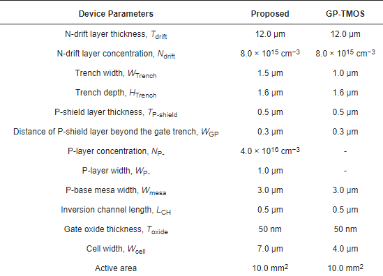
To create a depletion-mode pMOS, a lightly doped P-type layer is positioned between the P+ layer and the P-shield layer. In addition, the poly-Si gate is split into two parts, called the main gate (MG) and the auxiliary gate (AG). The MG controls the n-MOS, while the AG controls the D-pMOS. The two device structures share the device parameters as those listed in Table 1.
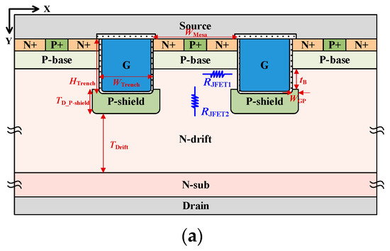
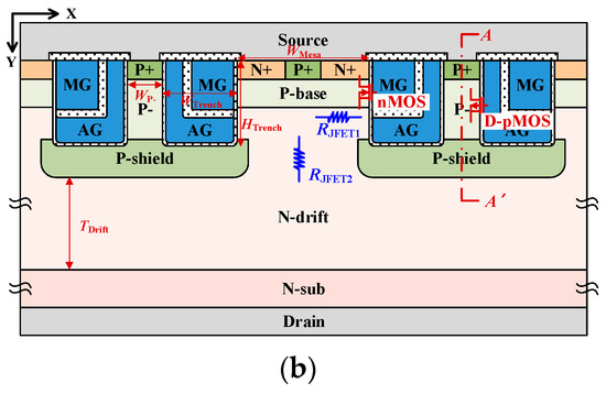
Figure 1. Cross-sectional views of (a) the conventional GP-TMOS, and (b) the proposed TMOS.
Table 1. Device parameters for TCAD simulations.
The RJFET of the GP-TMOS consists of two parts, as shown in Figure 1a. RJFET1 is formed between the P-base and P-shield, and RJFET2 is formed between adjacent P-shield layers. They can be expressed as

Here, WGP is the horizontal distance of the P-shield layer beyond the gate trench. WD_P-shield is the depletion region width of the P-shield/N-drift junction. WD_P-base is the depletion region width of the P-base/N-drift junction. tB is the vertical distance between P-base and P-shield. TP-shield is the thickness of the P-shield layer. VD is the potential of the P-shield/N-drift junction. According to Equation (3), the P-shield layer potential VD determines the extent of the depletion region in the JFET region of TMOS.
In the forward on-state, the P-shield layer of the proposed TMOS is disconnected from the source electrode by turning off the D-pMOS, and its potential is affected and increased by the voltage of the AG. Figure 2 shows the current density distributions for the GP-TMOS and the proposed TMOS at VMG = 18 V and VAG = 18 V. In the linear operation (Vds = 1 V), the depletion region width (WD) of the P-shield/N-drift junction for the proposed TMOS is smaller than that of the GP-TMOS, as illustrated in Figure 2a,b.
The current path width of the proposed TMOS is widened to decrease RJFET. In the saturation operation (Vds = 800 V), WD for the proposed TMOS is the same as that of the GP-TMOS, as well as the current path width in a single-cell pitch, as shown in Figure 2c,d. This indicates that RJFET1 and RJFET2 of the proposed TMOS are equal to those of the GP-TMOS in a single-cell pitch. Due to a relatively large cell pitch, the saturation current (Jsat) of the proposed TMOS can be remarkably reduced for the same active area. Thus, the proposed TMOS achieves a superior tradeoff relationship between RON, sp and SC capability.
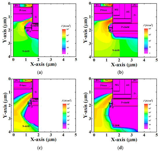
Figure 2. Current density distributions of two devices. (a) GP-TMOS at Vds = 1 V; (b) the proposed TMOS at Vds = 1 V; (c) GP-TMOS at Vds = 800 V and (d) the proposed TMOS at Vds = 800 V.
Figure 3a depicts the energy band diagram of the sandwiched P-type layers along the cutline A-A’ (shown in Figure 1b). When VAG = 0 V, the hole barrier between the P+ layer and the P-shield layer is small. The lightly doped P- layer can transport holes from the P-shield to P+, as shown in Figure 3b, indicating that the P-shield layer is grounded.
When VAG = 18 V, the EV from the P-shield layer to the P- layer decreases, resulting in a hole barrier. This is because the lightly doped P-layer is completely depleted, preventing holes’ transportation from the P-shield layer to the P+ layer, as shown in Figure 3c. This means that the P-shield layer is disconnected from the source electrode and is floating.
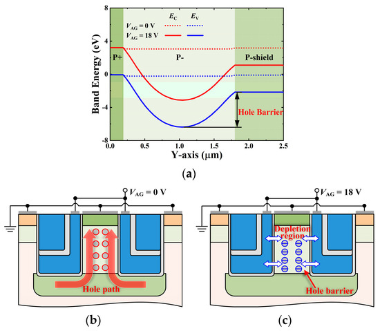
Figure 3. (a) Energy band diagram of the sandwiched P-type layers along the cutline A-A’, and operation mechanisms at (b) VAG = 0 V and (c) VAG =18 V.
In the blocking voltage state, the P-shield layer of the proposed TMOS is connected to the source electrode by turning on the D-pMOS, similar to that of the GP-TMOS. The grounded P-shield layer protects the gate oxide from the high electric field, and then maintains a reliable blocking high voltage capability.
During the switching transient, the P-shield layer of the proposed TMOS is also connected to the source electrode for safe operation. This is because the TMOS with floating P-shield layers has a notorious drawback, which is called dynamic on-resistance degradation. The proposed TMOS has an additional gate electrode, but only one set of gate drivers is required, as shown in Figure 4a.
Using two gate drive resistances, RAG-g and RMG-g, nMOS and D-pMOS can operate asynchronously. Figure 4b shows the waveforms of the MG voltage and AG voltage. The D-pMOS is set to turn off after the nMOS has turned on, keeping the P-shield layer grounded during the switching transient for reliable dynamic operation.
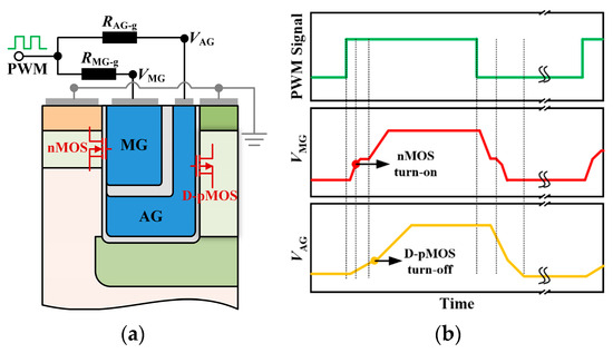
Figure 4. (a) Simplified diagram of the gate driver principle; (b) waveforms of two gate voltages.
3. Simulation Results and Discussion
The physical models include recombination models, incomplete ionization models, mobility models, bandgap narrowing models, and impact ionization models. It is noted that the Giga module is employed to capture self-heating effects and thermoelectric powers. The channel mobility of the TMOS is fixed to 50 cm2/V·s. In this comparison, the numerical simulation parameters are identical.
Figure 5 shows the impact of the width, WP-, and the doping concentration of the lightly doped P- layer, NP-, on the RON, sp (VMG = 18 V, VAG = 18 V and Jds = 200 A/cm2) and Jsat (VMG = 18 V, VAG = 18 V and Vds = 800 V) values of the proposed TMOS. As WP- and NP- decrease, RON, sp decreases and then remains at a fixed value. This is because the electrical connection state of the P-shield layer changes from grounded to floating. A small WP- and a low NP- facilitate the depletion of the P- layer. In contrast, Jsat increases as WP- and NP- decrease. The maximum Jsat is still below 6.5 kV/cm2 due to the relatively large cell pitch for the proposed TMOS.
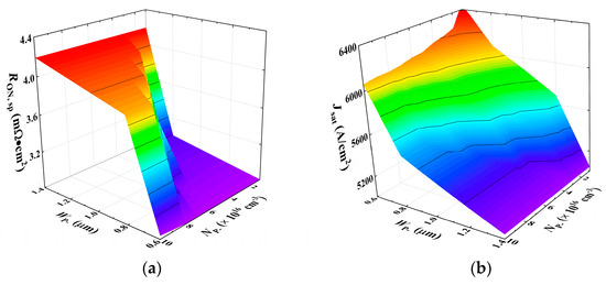
Figure 5. Impact of WP- and NP- on (a) RON, sp and (b) Jsat for the proposed TMOS.
Figure 6 shows the forward output characteristics for the proposed TMOS and the GP-TMOS. The WP- and NP- of the proposed TMOS are 1.0 μm and 4.0 × 1016 cm−3. The RON, sp of the proposed TMOS and the GP-TMOS is 2.95 mΩ·cm2 and 2.53 mΩ·cm2 with Vgs = 18 V and Jds = 200 A/cm2, respectively. The RON, sp of the proposed TMOS is approximately 10% higher than that of the GP-TMOS, whereas the Jsat of the proposed TMOS is substantially reduced from 10.22 kA/cm2 to 5.85 kA/cm2, a reduction of nearly 43%.
Figure 7 shows the blocking voltage characteristics. The P-shield layer of the proposed TMOS is grounded (VMG = 0 V and VAG = 0 V). The blocking behavior of the proposed TMOS is similar to that of the GP-TMOS. The maximum electric field of both is located at the P-shield/N-drift junction.
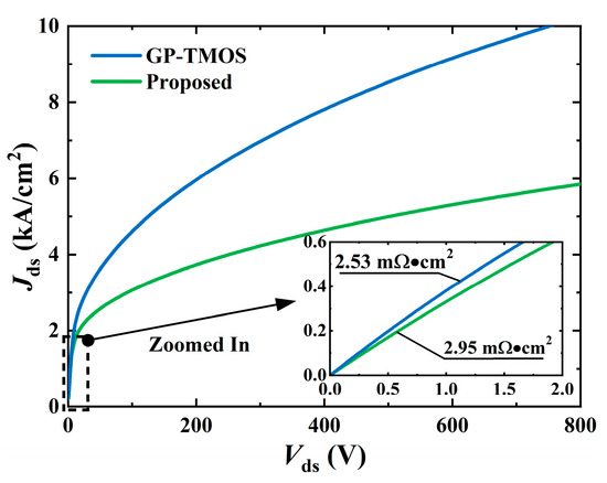
Figure 6. The output characteristics of the proposed TMOS and the GP-TMOS.
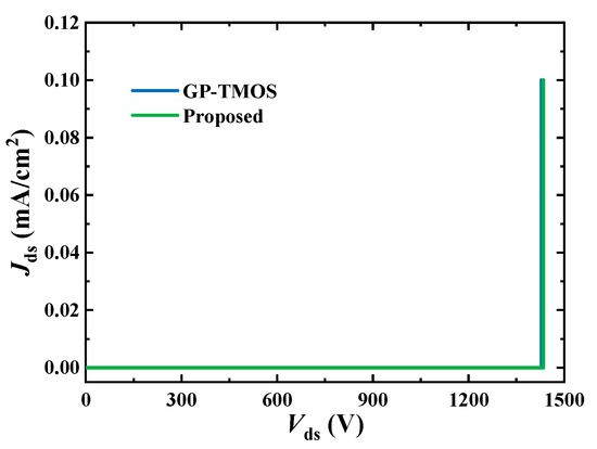
Figure 7. The blocking characteristics of the proposed TMOS and the GP-TMOS.
Figure 8 displays the SC-simulated waveforms of the current density, Jds, and the temperature profile for both the proposed TMOS and the GP-TMOS with Vgs = 18 V and Vds = 800.0 V. The peak current density of the proposed TMOS is decreased by 30%. Therefore, the junction temperature of the proposed TMOS is also lower, which could postpone the triggering of thermal runaway. Compared to the GP-TMOS, the SC withstanding time (tSC) of the proposed TMOS increases from 5.2 μs to 10.0 μs, which is approximately 1.92 times longer. The new design concept significantly eases the tension between RON, sp and tSC.
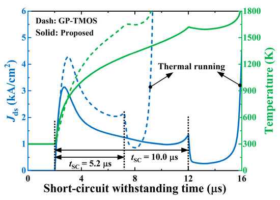
Figure 8. Short-circuit waveforms of the proposed TMOS and the GP-TMOS.
Figure 9 shows the schematic diagram of the dynamic switching simulation. The switching voltage and current are set to 800.0 V and 20.0 A, respectively. The stray inductance in the power loop is 5 nH. Figure 10 shows the influences of the AG resistance, RAG-g, and the doping concentration of the P-layer, NP-, on the power loss of the proposed TMOS. The power loss includes turn on loss and turn off loss. The RMG-g is set to 5, 10, and 20 Ω, and the dependence relationships are shown in Figure 10a–c. As NP- and RAG-g increase, the power loss decreases for various RMG-g.
This is caused by the change in the P-shield layer’s connection state during the switching transient, from a floating state to a grounded state. The TMOS with floating P-shield layers has poor dynamic performance and exhibits relatively higher switching loss. As NP- increases, a relatively high AG voltage is required to fully deplete the P-layer, which affects the threshold voltage of the D-pMOS. On the other hand, increasing RAG-g delays the triggering of the D-pMOS’s turn off during the turn on stage of the proposed TMOS. Both of the above methods can achieve grounded P-shield layers during the switching on transient of the proposed TMOS.
Figure 11 shows the switching waveforms of the proposed TMOS under two conditions. Condition I is NP- = 1 × 1016 cm−3 and RAG-g = 1 Ω, while condition II is NP- = 4 × 1016 cm−3 and RAG-g = 20 Ω. Under condition I, the D-pMOS turns off before the nMOS turns on. The turn on behavior of the proposed TMOS is the same as that of the TMOS with floating P-shield layers, where the expanding depletion region of the P-shield/N-drift junction cannot shrink back immediately, resulting in a slower switching speed and dynamic RON degradation. Under condition II, the D-pMOS turns off after the nMOS turns on. The switching performance is obviously improved by grounding the P-shield.
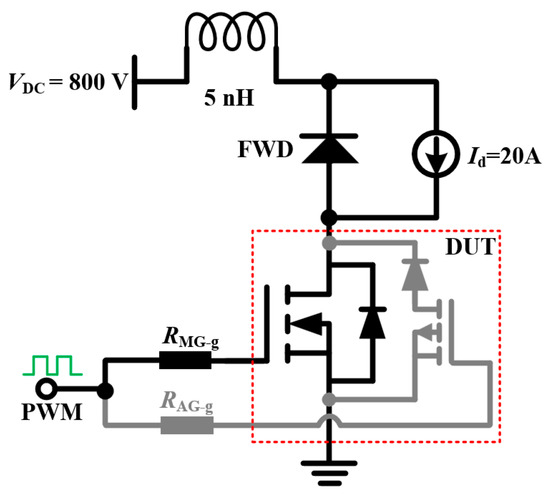
Figure 9. The schematic diagram of the dynamic switching simulation.
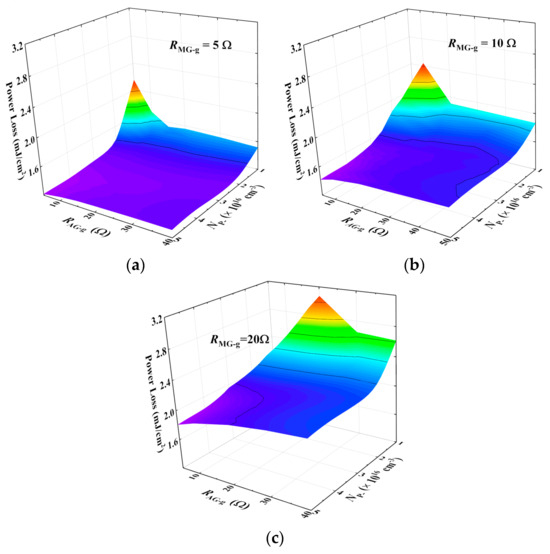
Figure 10. Influences of RAG-g and NP- on the power loss, when (a) RMG-g = 5 Ω, (b) RMG-g = 10 Ω, and (c) RMG-g = 20 Ω.
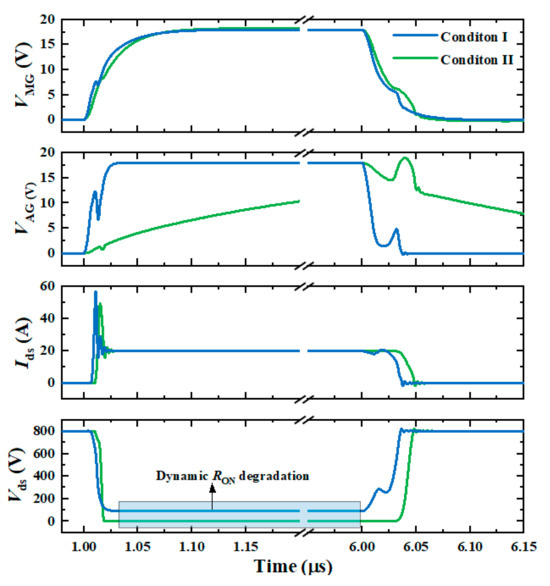
Figure 11. Switching waveforms of the proposed TMOS for condition I (NP- = 1 × 1016 cm−3, RAG-g = 1 Ω) and condition II (NP- = 4 × 1016 cm−3, RAG-g = 20 Ω).
Figure 12 compares the switching waveforms for the proposed TMOS and the GP-TMOS. Both the gate resistance of the GP-TMOS and the MG resistance of the proposed TMOS are set to 10 Ω. The NP- and RAG-g of the proposed TMOS are 4.0 × 1016 cm−3 and 5 Ω, respectively. The optimized AG resistance ensures a reliable switching operation without dynamic RON degradation. Moreover, the switching speed of the proposed TMOS is improved, due to the split-gate structure.
The proposed TMOS exhibits a shorter switching time as a result of its lower gate drain capacitance. The tON and tOFF of the SFP-SG-MOSFET are both smaller than those of the GP-TMOS and decrease by 48.7% and 74%, respectively. The switching power losses are calculated as shown in Figure 13. The turn on loss (EON) for the proposed TMOS is 1.05 mJ/cm2, which is reduced by about 35.5% compared to the GP-TMOS. The turn off loss (EOFF) for the proposed TMOS is 0.38 mJ/cm2, which is reduced by about 50% compared to that of the GP-TMOS.
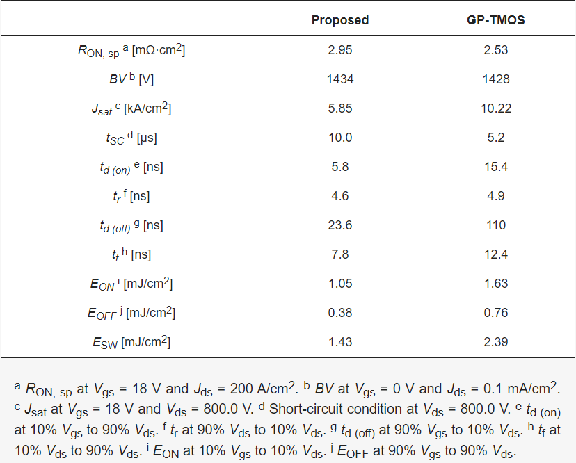
The total switching loss (ESW) for the proposed TMOS is as low as 1.43 mJ/cm2, showing a 40% reduction compared to that of the GP-TMOS. The performance comparison of the two devices is offered in Table 2.
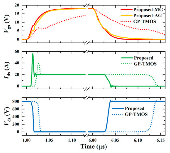
Figure 12. Switching waveforms of the proposed TMOS and the GP-TMOS.
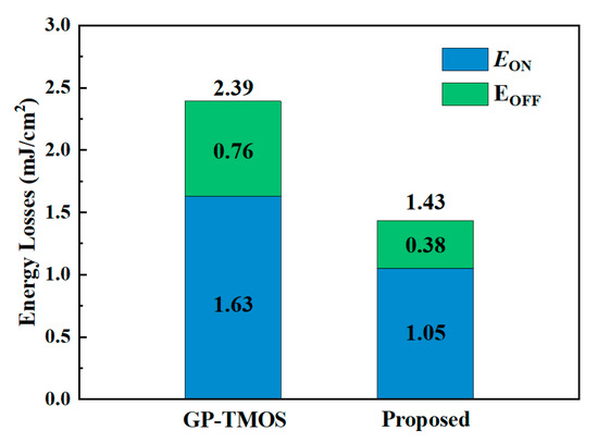
Figure 13. Switching losses of the proposed TMOS and the GP-TMOS.
Table 2. Comparison of two structure device characteristics.
4. Conclusions
A novel 4H-SiC-trench MOSFET with a depletion-mode pMOS (D-pMOS) is proposed and investigated numerically. Using the D-pMOS, the potential of the P-shield layer of the proposed TMOS can be controlled using an auxiliary gate. The width of the depletion region of the P-shield/N-drift junction is adaptively modulated in the linear and saturation operating regions.
Consequently, the proposed TMOS acquires a superior RON, sp—tSC tradeoff, achieving a 92% longer short-circuit withstanding time than that of the GP-TMOS. Moreover, the proposed TMOS flexibly utilizes two different gate resistances, while using only one set of gate drivers, which suppresses the dynamic RON degradation and further reduces switching loss. It achieves a 40% lower switching loss than that of the GP-TMOS. The superior SC capability and lower switching dissipation of the proposed TMOS hold the promise of enhancing the efficiency and reliability of power electronic systems.
Authors
Hengyu Yu, Limeng Shi, Monikuntala Bhattacharya, Michael Jin, Jiashu Qian, Anant K. Agarwal
Original – MDPI
-
Navitas Semiconductor invites visitors to experience “Planet Navitas” and collaborate to “Electrify Our World” at APEC 2024 (Long Beach, CA, February 26th-29th, 2024).
Since its inception in 1985, the Applied Power Electronics Conference (APEC) has become the world’s premier event in power electronics, with high-caliber, peer-reviewed technical content from industry and academia. The APEC 2016 keynote by Dan Kinzer, COO / CTO and co-founder, was the public debut for start-up Navitas and GaNFast power ICs.
Following the mission to “Electrify our World™”, the “Planet Navitas” exhibition booth invites visitors to discover how next-gen GaN and SiC technology enable the latest solutions for fully-electrified housing, transportation and industry. Examples range from TV power to home-appliance motors and compressors, EV charging, solar/micro-grid installations, and on to data center power systems. Each example highlights end-user benefits, such as increased portability, longer range, faster charging, and grid-independence, plus a focus on how low-carbon-footprint GaN and SiC technology can save over 6 Gtons/yr CO2 by 2050.
“APEC is a significant event in the power industry calendar, with an intense schedule of customer discussions on new technologies and systems,” said Mr. Kinzer. “Complementary GaNFast™ and GeneSiC™ portfolios, with comprehensive, application-specific system design support accelerates customer time-to-market with sustainable performance advantages. ‘Planet Navitas’ represents the very real, inspiring implementation of GaN & SiC across the vast $22B/year market opportunity.”
Major technology updates and releases include GaNSafe – the world’s most-protected, most-reliable and highest-performance GaN power, Gen-4 GaNSense Half-Bridge ICs – the most integrated GaN devices, Gen-3 Fast SiC power FETs – for high-power performance, and breakthrough bi-directional GaN for game-changing motor drive and energy-storage applications.
APEC 2024 will take place at the Long Beach Convention & Entertainment Center, 300 East Ocean Boulevard, Long Beach, CA 90802, with exhibition running from February 26th – 28th. “Planet Navitas” is featured at booth #1353.
Technical presentations:
- Tuesday 27th February
- “Reducing System Cost with GaN HEMTs in Motor Drive Applications”
- 8:55am, IS05.2, Alfred Hesener, Sr. Dir. Industrial & Consumer
- 10:40am, PSTT02.6, Bin Li, Dir. Applications
- 11:40am, PSTT01.9, Xiucheng Huang, Sr. Director
- 3:45pm, exhibitor presentation, location: 101B
- “Reducing System Cost with GaN HEMTs in Motor Drive Applications”
- Thursday 29th February
- “SiC & Package Innovations in Power Modules”
- 8:30am-11:20am, IS19, Stephen Oliver, Session Chair.
- 8:55am, PSTIS21.2, Tom Ribarich, Sr Dir. Strategic Marketing
- 1:30pm-3:10pm, IS27, Llew-Vaughan-Edmunds, Session Chair
- 2:20pm, IS27-3, Stephen Oliver, VP Corp Mktg & IR, and Llew Vaughan-Edmunds, Sr Dir. GeneSiC
- “SiC & Package Innovations in Power Modules”
Student Job Fair:
- From Los Angeles to Shanghai, careers at Navitas span cutting-edge IC design and innovative applications engineering to pioneering research and ensuring customer success and revenue growth. Meet the experts and join the team!
- Tuesday, February 27, 1:30pm-5pm, Regency Ballroom ABC of the Hyatt Regency hotel, right next to the Long Beach Convention Center, with Shaun Sandera, Sr. Human Resources Manager
To schedule a meeting with the Navitas team, email info@navitassemi.com, or select from the bookings calendars below:
Customer (Private Room): https://bit.ly/navitas-apec-24-customer-private-room
Customer Meeting (On-Booth): https://bit.ly/navitas-apec-24-customer-on-boothOriginal – Navitas Semiconductor
- Tuesday 27th February
-
GaN / LATEST NEWS / WBG3 Min Read
Navitas Semiconductor and SHINRY, global industry leader of on-board power supply and strategic supplier to Honda, Hyundai, BYD, Geely, XPENG, BAIC and many more leading automobile manufacturers, announced the opening of an advanced, joint R&D power laboratory to accelerate the development of New-Energy Vehicle (NEV) power systems enabled by Navitas’ GaNFast™ technology.
Next-gen gallium nitride (GaN) is replacing legacy silicon power chips due to superior high-frequency and high-efficiency characteristics. GaN delivers faster charging, faster acceleration and longer-range, accelerating market adoption of NEVs and the transition from fossil fuels to clean, renewable energy.
On January 16th, 2024, Peter (Jingjun) Chen, COO of SHINRY, along with Navitas’ Gene Sheridan, CEO and Navitas’ Charles (Yingjie) Zha, VP and GM plus other senior executives attended the joint lab’s opening ceremony at SHINRY headquarters in Shenzhen.
The joint lab accelerates development projects, with leading-edge GaN technology combining with innovative system-design skills and engineering talent to enable unprecedented high power density, lightweight, efficient designs that translate to faster charging and extended range, with faster time-to-market.
The joint lab brings together experienced, highly-professional engineers from Navitas and SHINRY to build efficient, collaborative R&D platforms. Navitas’ own dedicated EV system Design Center, located in Shanghai will provide comprehensive technical support for the joint lab.
Navitas will not only supply SHINRY with leading-edge, trusted power devices, but will also engage in system-level R&D from the initial stages of product specification and design, through to test platforms and customized packaging solutions. The result will be more efficient, higher power density, more reliable, and cost-effective power systems for NEVs.
“SHINRY always pursues technological innovation. As early as 2012, SHINRY began applying Silicon Carbide (SiC) MOS, and in 2019, SHINRY initiated research on the application of GaN and has been actively seeking strategic partners.” said Peter (Jingjun) Chen, COO of SHINRY.
“As an advanced supplier in the field, Navitas will assist in creating more advanced, energy-efficient, and higher-efficiency power system products. I believe the establishment of this joint lab will comprehensively accelerate the design and market launch of SHINRY’s products and further enhance the market competitiveness of SHINRY products.”
“We are excited to join with SHINRY to establish a new lab for next-gen power semiconductors, assisting SHINRY in creating advanced power systems.” said Gene Sheridan, Navitas’ co-founder & CEO. “SHINRY’s mission to change the way of travel aligns closely with Navitas’ Electrify Our World™ mission. We believe that through our joint efforts, leading GaN technologies will enter the power systems of NEVs for more end-users, contributing to the vigorous growth of the new energy industry.
Original – Navitas Semiconductor
-
STMicroelectronics N.V. reported U.S. GAAP financial results for the fourth quarter ended December 31, 2023. STMicroelectronics reported fourth quarter net revenues of $4.28 billion, gross margin of 45.5%, operating margin of 23.9%, and net income of $1.08 billion or $1.14 diluted earnings per share.
Jean-Marc Chery, STMicroelectronics President & CEO, commented:
- “FY23 revenues increased 7.2% to $17.29 billion. Operating margin was 26.7% compared to 27.5% in FY22 and net income increased 6.3% to $4.21 billion. We invested $4.11 billion in net CAPEX while delivering free cash flow of $1.77 billion.”
- “In Q4, ST delivered revenues and gross margin slightly below the mid-point of the guidance, with higher revenues in Personal Electronics offset by a softer growth rate in Automotive.”
- “In Q4, our customer order bookings decreased compared to Q3. We continued to see stable end-demand in Automotive, no significant increase in Personal Electronics, and further deterioration in Industrial.”
- “Our first quarter business outlook, at the mid-point, is for net revenues of $3.6 billion, decreasing year-overyear by 15.2% and decreasing sequentially by 15.9%; gross margin is expected to be about 42.3%.”
- “For 2024, we plan to invest about $2.5 billion in net CAPEX.”
- “We will drive the Company based on a plan for FY24 revenues in the range of $15.9 billion to $16.9 billion. Within this plan, we expect a gross margin in the low to mid-40’s.”
Original – STMicroelectronics
-
Acquired by Infineon Technologies in October 2023, GaN Systems has been recognized as the “Graduate Of The Year” by The Global Cleantech 100. The announcement was made at Cleantech Forum North America in San Francisco.
The award recognizes the exceptional contribution legacy GaN Systems has made to sustainable innovation and their successful management team as rated by the financial investors on the 80-member Cleantech Group Expert Panel. This 2024 award rounds out several years of recognition in GaN Systems’ sustainability journey which includes entry in to the Global Cleantech 100 Hall of Fame (1 of only 14 companies ever) and the 2023 Global Cleantech 100 winner (1 of only 100 companies globally in 2023).
The acquisition of GaN Systems has significantly accelerated Infineon’s gallium nitride (GaN) roadmap and further strengthens its leadership in power systems by offering a broad product portfolio combined with leading edge application know-how in the development of GaN-based solutions. Infineon’s expertise and in-depth knowledge in GaN paves the way for more energy-efficient and CO 2-saving technology solutions that support decarbonization.
“My congratulations go out to all legacy GaN Systems employees for this recognition and winning multiple Cleantech awards. We are glad to have these smart and curious minds on board at Infineon,” said Adam White, Division President at Power & Sensor Systems at Infineon. “Thanks to unrivalled R&D resources, a comprehensive understanding of applications and a large number of customer projects, Infineon now leverages the full potential of GaN Systems to become a leading GaN Powerhouse fostering the transformation towards green energy.”
Cleantech® Group is a leading global authority on global cleantech innovation. The Global Cleantech 100 program has been running since 2009. This highly anticipated annual report publishes a list of companies with the most promising ideas in cleantech.
Original – Infineon Technologies
-
GaN / LATEST NEWS / SiC / WBG2 Min Read
Infineon Technologies AG announced its joint Innovation Application Center in Shenzhen with Anker Innovations, a global leader in charging technology. With the center already fully operating, it is paving the way for more energy-efficient and CO2-saving charging solutions that support decarbonization.
Driven by the growing consumer demand for faster charging solutions due to an increasing usage of mobile devices, laptops and other battery-powered devices, the idea of establishing an Anker-Infineon Innovation Application Center dated back to 2021. After two years of preparation, the joint lab now serves as R&D hub for industry experts to develop power-delivery (PD) fast charging solutions with higher power density, mainly based on Infineon’s next-generation Hybrid Flyback (HFB) controller product family and the CoolGaN™ IPS for fast chargers above 100W.
Anker has already brought several successful products to the market, such as the industry-leading 100W+ fast charger device powered by Infineon’s CoolGaN in 2022. With the Innovation Application Center Anker and Infineon will even shorten the application cycle and accelerate the time to market for future products.
“Anker is an important customer for Infineon,” said Christian Burrer, Vice President of Systems & Application Marketing of Power & Sensor Systems Division at Infineon Technologies. “We have already started a strong cooperation in the charging field, with product and system solutions covering several Infineon product lines. In the field of PD charging, we provide our customers a comprehensive product portfolio, including state-of-the-art power controllers, first-class switching power supplies, leading silicon MOSFET and GaN transistor performance, and more.”
Beyond charging solutions, the joint lab is focusing on a more diversified range of consumer applications, driven by Infineon’s expertise in wide-bandgap materials such as gallium nitride (GaN). The acquisition of GaN Systems in 2023 has significantly accelerated Infineon’s GaN roadmap and further strengthens its leadership in power systems through mastery of all relevant power semiconductor technologies.
“In 2023, Anker achieved success in many markets such as China and Europe. This would not have been possible without Infineon’s GaN technology solutions and the strong collaboration between our companies. We look forward to even intensifying our partnership with Infineon”, said by Kang Xiong, General Manager of the charging business unit at Anker Technologies.
Original – Infineon Technologies