-

Veeco Instruments Inc. announced financial results for its third quarter ended September 30, 2024. Results are reported in accordance with U.S. generally accepted accounting principles (“GAAP”) and are also reported adjusting for certain items (“Non-GAAP”). A reconciliation between GAAP and Non-GAAP operating results is provided at the end of this press release.
Third Quarter 2024 Highlights:
- Revenue of $184.8 million, compared with $177.4 million in the same period last year
- GAAP net income of $22.0 million, or $0.36 per diluted share, compared with $24.6 million, or $0.42 per diluted share in the same period last year
- Non-GAAP net income of $28.3 million, or $0.46 per diluted share, compared with $31.0 million, or $0.53 per diluted share in the same period last year
“Veeco reported solid third quarter results above the mid-point of our guidance, led by record Semiconductor revenue,” commented Bill Miller, Ph.D., Veeco’s Chief Executive Officer. “Our Semiconductor business grew 26% year-over-year and 13% sequentially, highlighted by an increase in shipments to leading-edge customers across several product lines. Our portfolio of enabling technologies is gaining traction for several industry inflections, contributing to our expectations for our Semiconductor business to outperform WFE growth for the 4th consecutive year.”
Original – Veeco Instruments
-

Vishay Intertechnology, Inc. announced results for the fiscal third quarter ended September 28, 2024.
Highlights
- 3Q 2024 revenues of $735.4 million
- Gross margin was 20.5% and included the negative impact of approximately 150 basis points related to the addition of Newport
- GAAP loss per share of ($0.14); adjusted EPS of $0.08 per share
- 3Q 2024 book-to-bill of 0.88 with book-to-bill of 0.79 for semiconductors and 0.97 for passive components
- Backlog at quarter end was 4.4 months
“For the third consecutive quarter this year, revenue has held fairly constant, reflecting a prolonged period of inventory de-stocking as the pace of consumption by industrial customers remains slow, backlogs are pushed out and macroeconomic conditions in Europe worsen,” said Joel Smejkal, President and CEO. “While the industry remains in a downcycle, we are making the necessary adjustments to manage costs while continuing to execute our five-year strategic plan. We are preparing to participate fully in the next industry up-cycle and we are putting the foundation in place to capitalize on the longer term demand catalysts of e-mobility and sustainability to drive faster revenue growth, and improve profitability and returns on invested capital.”
For the fourth quarter of 2024, management expects revenues in the range of $720 million +/- $20 million, with gross profit margin in the range of 20.0% +/- 50 basis points, including the negative impact of approximately 175 to 200 basis points from the addition of Newport.
Original – Vishay Intertechnology
-

Navitas Semiconductor has announced the world’s first 8.5 kW power supply unit (PSU), powered by GaN and SiC technologies to achieve 98% efficiency, for next-generation AI and hyperscale data centers.
The AI-optimized 54V output PSU complies with Open Compute Project (OCP) and Open Rack v3 (ORv3) specifications and utilizes high-power GaNSafe and Gen-3 Fast SiC MOSFETs configured in 3-phase interleaved PFC and LLC topologies, to ensure the highest efficiency and performance, with lowest component count. The PSU’s shift to a 3-phase topology for both the PFC and LLC (vs. 2-phase topologies used by competing PSUs) enables the industry’s lowest ripple current and EMI.
Furthermore, the PSU reduces the number of GaN and SiC devices by 25% compared with the nearest competing system, which reduces the overall cost. The PSU has an input voltage range of 180 to 264 Vac, a standby output voltage of 12 V, and an operating temperature range of -5oC to 45oC. Its hold-up time at 8.5 kW is 10 ms, with 20 ms possible through an extender.
The 3-Phase LLC topology is enabled by high-power GaNSafe, which is specifically created for demanding, high-power applications, such as AI data centers and industrial markets. Navitas’ 4th generation integrates control, drive, sensing, and critical protection features that enable unprecedented reliability and robustness. GaNSafe is the world’s safest GaN with short-circuit protection (350ns max latency), 2kV ESD protection on all pins, elimination of negative gate drive, and programmable slew rate control. All these features are controlled with 4-pins, allowing the package to be treated like a discrete GaN FET, requiring no VCC pin. Suitable for applications from 1 kW to 22 kW, 650 V GaNSafe in TOLL and TOLT packages are available with a range of RDS(ON)MAX from 25 to 98 mΩ.
The 3-Phase interleaved CCM TP-PFC is powered by Gen-3 Fast SiC MOSFETs with ‘trench-assisted planar’ technology, which has been enabled by over 20 years of SiC innovation leadership and offers world-leading performance over temperature, delivering cool-running, fast-switching, and superior robustness to support faster charging EVs and up to 3x more powerful AI data centers.
“This complete wide bandgap solution of GaN and SiC enables the continuation of Navitas’ AI power roadmap which enables this 8.5kW and plans to drive to 12kW & higher in the near-term”, said Gene Sheridan, CEO and co-founder of Navitas. “As many as 95% of the world’s data centers cannot support the power demands of servers running NVIDIA’s latest Blackwell GPUs, highlighting a readiness gap in the ecosystem. This PSU design directly addresses these challenges for AI and hyperscale data centers.”
The PSU will be on display for the first time at Electronica 2024 (Hall C 3, booth 129, November 12th– 15th).
Original – Navitas Semiconductor
-

GlobalFoundries Inc. (GF) announced preliminary financial results for the third quarter ended September 30, 2024.
Key Third Quarter Financial Highlights
- Revenue of $1.739 billion
- Gross margin of 23.8% and Non-IFRS gross margin of 24.7%
- Operating margin of 10.6% and Non-IFRS operating margin of 13.6%
- Net income of $178 million and Non-IFRS net income of $229 million
- Non-IFRS adjusted EBITDA of $627 million
- Cash, cash equivalents and marketable securities of $4.3 billion
- Year to date net cash provided by operating activities of $1,265 million and Non-IFRS adjusted free cash flow of $779 million
“In the third quarter, the GF team continued to execute next generation opportunities with our customers, by securing key design wins across our growing portfolio of essential chip technologies,” said Dr. Thomas Caulfield, President and CEO of GF. “We delivered consistent financial results at the upper end of the guidance ranges we provided in our August earnings release, and as we continue to navigate the ongoing uncertainties facing our industry, we remain on-track to deliver approximately a threefold increase in our year-over-year Non-IFRS adjusted free cash flow generation by the end of 2024.”
Recent Business Highlights
- Building on the longtime relationship between GF and NXP Semiconductors (NXP), the companies announced a new collaboration leveraging GF’s 22FDX® process technology platform and global manufacturing footprint to optimize the power, performance and time-to-market of NXP’s solutions across a range of automotive, IoT and smart mobile devices. GF’s 22FDX chips will be manufactured in Dresden, Germany and Malta, New York, providing NXP geographically diverse supply for their customers.
- Over one thousand customers and partners attended GF’s annual Technology Summit held around the world in Santa Clara, California, Munich, Germany and Shanghai, China, to build deeper relationships and learn how GF’s essential chips play a critical role in realizing “AI Everywhere.”
- GF entered into a strategic technology development and licensing agreement with Finwave Semiconductor, Inc (Finwave), a leading innovator in GaN technology. The collaboration will optimize and scale Finwave’s cutting-edge GaN-on-Si technology to volume production at GF’s 200mm fab in Burlington, Vermont.
Original – GlobalFoundries
-

STMicroelectronics inaugurated its new design and industrialization center, equipped with a test lab, in Pisa Montacchiello, Italy. The CEO of STMicroelectronics Italy, Lucio Colombo, and the Rector of the University of Pisa, Riccardo Zucchi, cut the ribbon of the new center, the thirteenth ST site in Italy and the first in Tuscany.
The center, built in collaboration with professors from the University of Pisa’s Department of Information Engineering, currently houses around 40 people mainly dedicated to the design and industrialization of integrated circuits. They include analog and digital designers with different skills, together with researchers and thesis students from the University of Pisa.
Most of the designers belong to ST’s APMS Product Group’s Analog Custom Devices (ACD) division, which works on the design and development of products for the consumer electronics market. In particular, the Pisa team of the ACD division focuses on products for wireless charging and power management. Their goal is to identify and implement innovative solutions to improve the efficiency of battery-powered devices like smartphones. The center is equipped with a test lab to carry out the validation and industrialization of the products developed on-site.
In addition to inaugurating and visiting the center, Riccardo Zucchi and Lucio Colombo signed a framework agreement, the purpose of which is to – support the training of qualified students and graduates by collaborating on teaching courses for the University and by setting up scholarships in line with current regulations;
– contribute to studies and research focused on technological innovation within the center’s areas of expertise and interest;
– to uphold the high cultural standards of its operators and promote their professional development through meaningful contacts and cooperation with the University through courses guaranteed by the University.“The Pisa Center was born 20 months ago with the aim of growing quickly by acquiring talent in the area, thanks to the collaboration with the University of Pisa, but also by attracting talent eager to return to Tuscany in search of the job opportunities offered by a global leader,” said Lucio Colombo, CEO of STMicroelectronics Italy. “This is a model that ST has applied over the years at Italian universities close to its research and production centers.”
“The goal was to reach around 40 employees in two years and to date we are satisfied with the progress made. The Center relies on electronics engineers with mixed skills: analog/digital/software and testing, and with different seniority, together with researchers and thesis students,” explains Patrizia Milazzo, ACD Director, STMicroelectronics. “We believe that the rapid development of the center was made possible through the great collaboration with the University and the determination of ST colleagues, who were strongly dedicated to creating a center of excellence in Tuscany.”
Original – STMicroelectronics
-

SemiQ will exhibit its latest SiC power solutions for high-voltage applications at electronica 2024, the world’s leading electronics trade fair and conference, in Munich from November 12-15.
Visitors to SemiQ will be able to explore the company’s latest advancements in high-voltage technology. This includes the debut of the next generation of 1200V SiC MOSFETs and SemiQ’s QSiC portfolio of ultra-efficient modules, supporting innovations in EVs, renewable energy, motor drives, medical power supplies and high-power solar applications.
Engineered with high-performance ceramics, QSiC™ MOSFET modules offer industry-leading reliability in a compact form factor and have been designed to specifically meet the stringent demands for high-power, high-frequency applications. Each module undergoes wafer-level gate burn-in testing to ensure high-quality gate oxide and stable gate threshold voltage.
Dr. Timothy Han, President of SemiQ said: “Our solutions significantly enhance the performance and efficiencies necessary to propel the industry forward, unlocking yet more high-power applications. We look forward to demonstrating how these innovative technologies will pave the way for fresh designs and advancements in the industry.”
Electronica will take place at the Messe München in Munich, Germany, from November 12-15, 2024. SemiQ’s stand is at Alfatec’s booth in Hall A5, Booth 421.
Original – SemiQ
-
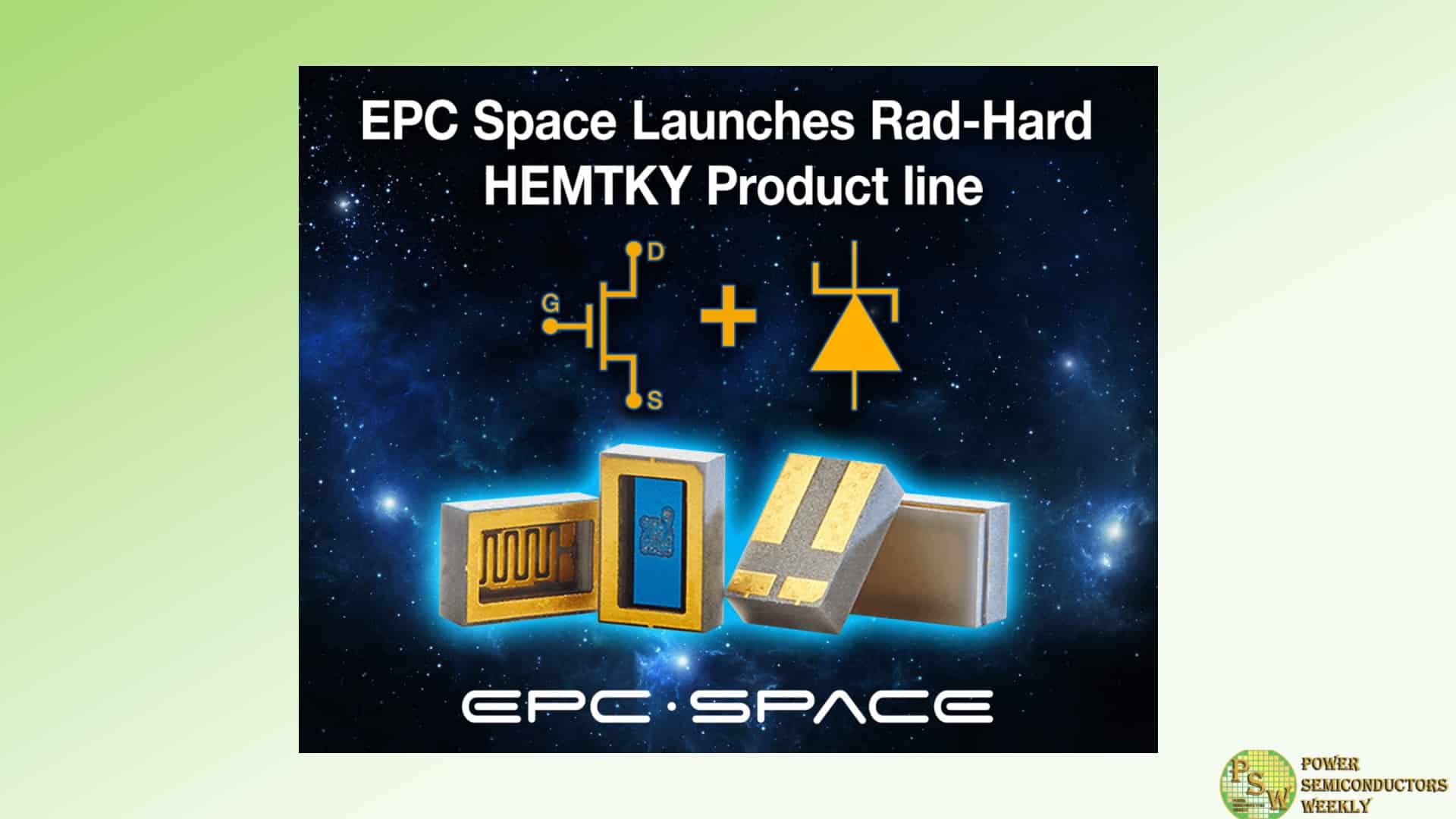
EPC Space announced the launch of HEMTKY product line.
A HEMTKY is a HEMT, High Electron Mobility Transistor, with an embedded Schottky diode. The presence of an antiparallel Schottky diode in the HEMTKY structure minimizes third quadrant conduction losses absent GaN HEMT synchronous drive. Notable advantages are:
- Predictable conduction losses, no reverse recovery charge
- Reduced system sensitivity to half-bridge deadtime variance
- Reduced negative voltage stress on gate drivers
For 500-unit quantities, engineering models are priced at $212 USD each, while space level units are priced at $315 USD each.
EPC Space provides revolutionary high-reliability radiation-hardened enhancement-mode gallium nitride power management solutions for space and other harsh environments. Radiation hardened GaN-based power devices address critical spaceborne environments for applications such as power supplies, motor drives, ion thrusters, and more. eGaN is a registered trademark of Efficient Power Conversion Corporation, Inc.
Original – EPC Space
-

Nexperia announced that it has entered into a strategic partnership with KOSTAL, a leading automotive supplier, which will enable it to produce wide bandgap (WBG) devices that more closely match the exacting requirements of automotive applications. Under the terms of this partnership, Nexperia will supply, develop, and manufacture WBG power electronics devices which will be designed-in and validated by Kostal. The collaboration will initially focus on the development of SiC MOSFETs in topside cooled (TSC) QDPAK packaging for onboard chargers (OBC) in electric vehicles (EV).
KOSTAL Automobil Elektrik, with over a century of experience, is a key player in the global automotive industry. Nearly one in every two cars worldwide is equipped with KOSTAL’s products, including more than 4.5 million onboard chargers, contributing to advancements in electromobility. Ranked among the top 100 automotive suppliers globally, KOSTAL is recognized for its innovative, reliable, and cost-optimized solutions. Its long-standing partnerships with customers and employees reflect the company’s commitment to quality and collaboration.
“Nexperia has been a trusted supplier of silicon components to KOSTAL for many years and is delighted to enter into this strategic partnership that will now extend to wide bandgap devices”, according to Katrin Feurle, Senior Director and Head of SiC Discretes & Modules. “KOSTAL will assist in validating our devices in its charging applications, thereby providing us with the type of invaluable ‘real-world’ data that will allow us to further enhance their performance”.
“KOSTAL is extending its’ strategic SiC supply portfolio to support our growth path towards 2030 with a special dedication on E-Mobility applications for onroad and offroad applications” states Dr. Georg Mohr, Executive VP Purchasing & Supply Chain of the KOSTAL Group. “Under this strategic partnership, which reinforces our long- standing customer-supplier relationship, KOSTAL will leverage Nexperia’s expertise in wide bandgap technology, particularly their SiC MOSFETs, which we believe are among the best in the market. By sharing our insights from real-world EV charging applications, we aim to contribute to the development of even more optimized and tailored SiC devices that meet the specific demands of our next-generation solutions.”
Nexperia is among the few companies that is offering a comprehensive range of WBG semiconductor technologies, including SiC diodes and MOSFETs, as well as GaN e-mode and d-mode devices, alongside its established silicon portfolio. With a strong commitment to expanding its commercial WBG offerings, Nexperia is focused on delivering the most suitable products to meet the needs of an increasing range of applications. The company’s focus is to support the responsible use of electrical energy through innovative solutions. Nexperia continues to develop technologies that address the growing demand for efficiency and sustainability in power management.
Original – Nexperia
-

Navitas Semiconductor announced unaudited financial results for the third quarter ended September 30, 2024.
“I’m pleased to announce record sales in the mobile fast-charger market plus a completely new GaN platform for 48V AI data centers, EV and AI robotics applications in conjunction with a new, strategic, dual-sourcing partnership with Infineon,” said Gene Sheridan, CEO and co-founder.
`“Despite macro-economic challenges, we continue to grow faster than the market, and the new, low-voltage GaN platform not only opens up new strategic markets, but also brings customers dual-sourcing options from Navitas and Infineon for added confidence to accelerate adoption of GaN into new mainstream, high-volume applications.”
The company also announced a cost-reduction plan that is expected to save $2 million per quarter and streamline the organization with increased focus on AI data center, EV and mobile applications, accelerating the company’s path to profitability. The plan includes a 14% reduction in headcount (approximately 45 employees).
3Q24 Financial Highlights
- Revenue: Total revenue was $21.7 million in the third quarter of 2024, compared to $22.0 million in the third quarter of 2023, and $20.5 million in the second quarter of 2024.
- Loss from Operations: GAAP loss from operations for the quarter was $29.0 million, compared to a loss of $28.6 million for the third quarter of 2023 and a loss of $31.1 million for the second quarter of 2024. On a non-GAAP basis, loss from operations for the quarter was $12.7 million compared to a loss of $8.7 million for the third quarter of 2023, and a loss of $13.3 million in the second quarter of 2024.
- Cash: Cash and cash equivalents were $98.6 million as of September 30, 2024.
Market, Customer and Technology Highlights
- New, Low-voltage (LV) GaN Platform (80-200V): Optimized for 48V systems in AI data center, EV, and motor drive, sampling in Q4 2024, with strategic dual-sourcing partnership with Infineon Technologies. Common specifications (packaging, pin-out, footprint and IP) to accelerate customer adoption of GaN into high-volume, mainstream applications.
- AI Data Center: New 98%-efficient, 8.5 kW AI power supply reference design with high-voltage (HV) GaN+SiC architecture launched as well as proprietary IntelliWeave™ PFC control technique to deliver extreme power density demanded by NVIDIA’s Hopper-Blackwell-Rubin AI GPU roadmap. High-voltage GaNSafe power ICs and Gen-3 ‘Fast’ SiC devices are featured in over 60 active customer projects with direct customers such as Delta, GreatWall, Compuware and LiteON, supplying end-users like AWS, Azure and Google. Our data center production revenues started in Q3 as expected and will continue ramping throughout 2025.
- EV: Leading-edge, trench-assisted, planar-gate Gen-3 ‘Fast’ SiC devices now fully AEC Q101 (automotive) qualified and pushing beyond. Six new on-board and road-side charger design wins in Q3, expected to ramp in 2025 and 2026. Largest pipeline segment, with 200+ projects. New, LV GaN platform optimized for 48V battery EV applications.
- Mobile & Consumer: GaNSlim ICs achieved another 26 design wins in Q3. Three new tier-1 OEM wins expected to deliver revenue ramping Q2’25, adding to the Samsung wins announced in August.
- Appliance & Industrial: Thirty new design wins in Q3, ranging from vacuum cleaners and LED lighting, to solid-state, grid-connected circuit-breakers, multi-kW power supplies and heat pumps. New, LV GaN platform addresses 48V industrial motor drives including AI robotics.
- Solar & Energy Storage: Ten design wins, including at Generac, expected to ramp mid-2025. Next-gen GaN ICs – including Navitas-proprietary, industry-leading bi-directional GaN ICs – continue on track for significant mid-2025 ramp in solar micro-inverters. New, LV GaN doubles TAM in inverters, as complement to HV GaN and SiC.
Fourth quarter 2024 net revenues are expected to be between $18.0 and $20.0 million. Non-GAAP gross margin for the fourth quarter is expected to be 40% plus or minus 50 basis points and non-GAAP operating expenses are expected to be approximately $20.5 million in the fourth quarter of 2024.
Original – Navitas Semiconductor
-

NXP Semiconductors N.V. reported financial results for the third quarter, which ended September 29, 2024.
“NXP delivered quarterly revenue of $3.25 billion, in-line with our overall guidance. While we experienced some strength against our expectations in the Communication Infrastructure, Mobile and Automotive end markets, we were confronted with increasing macro related weakness in the Industrial & IoT market. Our guidance for the fourth quarter reflects broader macro weakness especially in Europe and the Americas. We focus on managing what is in our control enabling NXP to drive resilient profitability and earnings in an uncertain demand environment,” said Kurt Sievers, NXP President and Chief Executive Officer.
Key Highlights for the Third Quarter 2024:
- Revenue was $3.25 billion, down 5 percent year-on-year;
- GAAP gross margin was 57.4 percent, GAAP operating margin was 30.5 percent and GAAP diluted Net Income per Share was $2.79;
- Non-GAAP gross margin was 58.2 percent, non-GAAP operating margin was 35.5 percent, and non-GAAP diluted Net Income per Share was $3.45;
- Cash flow from operations was $779 million, with net capex investments of $186 million, resulting in non-GAAP free cash flow of $593 million;
- During the third quarter of 2024, NXP continued to execute its capital return policy with the payment of $259 million in cash dividends, and the repurchase of $305 million of its common shares. The total capital return of $564 million in the quarter represented 95 percent of third quarter non-GAAP free cash flow. On a trailing twelve month basis, capital return to shareholders represented $2.4 billion or 87 percent of non-GAAP free cash flow. The interim dividend for the third quarter 2024 was paid in cash on October 9, 2024 to shareholders of record as of September 12, 2024. On August 29th, the NXP board of directors authorized an additional $2.0 billion for share repurchases, resulting in a $2.64 billion share repurchase balance at the end of the third quarter. Subsequent to the end of the third quarter, between September 30, 2024 and November 1, 2024, NXP executed via a 10b5-1 program additional share repurchases totaling $117 million;
- On August 20, 2024, ESMC, the previously announced manufacturing joint venture between TSMC, Robert Bosch GmbH, Infineon Technologies AG and NXP Semiconductors N.V. held a groundbreaking ceremony to mark the initial phase of construction of its first semiconductor fab in Dresden, Germany;
- On September 4, 2024, Vanguard International Semiconductor Corporation and NXP Semiconductors N.V. announced the receipt of all necessary governmental approvals from relevant authorities and injected capital to officially establish the previously announced VisionPower Semiconductor Manufacturing Company Pte Ltd (VSMC) manufacturing joint venture. The company will now proceed with the planned construction of VSMC’s first 300mm wafer manufacturing facility;
- On September 10, 2024, NXP announced the Trimension® SR250, the industry’s first single-chip, UWB solution to enable Industrial and IoT applications that integrates on-chip processing capabilities with both short-range UWB-based radar and secure ranging;
- On September 17, 2024, NXP announced the MC33777, the world’s first electric vehicle battery junction box IC that consolidates essential BMS functions into a single device; and
- On September 24, 2024, NXP announced the new i.MX RT700 crossover MCU family, designed to power smart AI-enabled edge devices, such as wearables, consumer medical devices, smart home devices and HMI platforms.
Original – NXP Semiconductors
