-
 LATEST NEWS / PRODUCT & TECHNOLOGY / SiC / WBG
SemiQ Launches High-Efficiency 1200V SiC MOSFET Six-Pack Modules for Scalable, Compact Power Designs
April 16, 2025
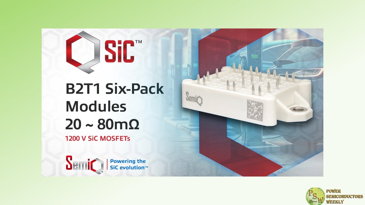
2 Min ReadSemiQ Inc has announced a series of highly efficient 1200 V SiC MOSFET Six-Pack Modules. These have been designed to enable lower cost and more compact system-level designs at large scale.
The rugged, high-speed switching SiC MOSFETs implement a planar technology with rugged gate oxide and feature a reliable body diode. These are arranged in a three-phase bridge topology, with the modules additionally featuring split DC negative terminals, press-fit terminal connections and a Kelvin reference for stable operation.
The high-power-density modules benefit from low switching losses, as well as low junction-to-case thermal resistance and all parts have been tested beyond 1350 V, with 100% wafer-level burn in (WLBI).
They have been developed for applications including AC/DC converters, energy storage systems, battery charging, motor drives and PFC boost converters, including EV fast charging, induction heating and welding, renewable energy supplies and UPS.
The modules are operational to 175oC junction temperature, and have been designed for easy mounting, including direct mounting to a heatsink. The product family has been launched with 20, 40 and 80mΩ variants (GCMX020A120B2T1P, GCMX040A120B2T1P, GCMX080A120B2T1P) that have a power dissipation of 263, 160 and 103 W respectively.
They conduct a continuous drain current of 29 – 30A, and a pulsed drain current of 70 A. Additionally, they have turn-on switching energy of 0.1- 0.54 mJ and a turn-off switching energy of 0.02 – 0.11 mJ, with a switching time of 56 – 105 ns.
The module is available immediately in a 62.8 x 33.8 x 15 mm package including heatsink mountings.
Original – SemiQ
-

Navitas Semiconductor has announced its high-power GaNSafe™ ICs achieve automotive qualification for both AEC-Q100 and AEC-Q101, showcasing GaN’s next inflection into the automotive market.
Navitas high-power GaNSafe 4th generation family integrates control, drive, sensing, and critical protection features that enable unprecedented reliability and robustness in high-power applications. It is the world’s safest GaN with short-circuit protection (350ns max latency), 2kV ESD protection on all pins, elimination of negative gate drive, and programmable slew rate control. All these features are controlled with 4-pins, allowing the package to be treated like a discrete GaN FET, requiring no VCC pin.
The Automotive Electronics Council (AEC) lists various qualifications focused on failure mechanism-based stress tests for packaged integrated circuits (AEC-Q100) and discrete semiconductors (AEC-Q101) used in automotive applications. Navitas’ GaNSafe™ has been qualified to both standards to ensure that both the discrete power FET stage and the combined IC solution meet these stringent specifications.
To support the qualification, Navitas has created a comprehensive reliability report that analyzes over 7 years of production and field data. It demonstrates their track record, alongside generational and family improvements in robustness and reliability, establishing GaN power ICs as highly reliable and automotive-ready. This reliability report is available to qualified customers.
Additionally in March 2025, Navitas unveiled the world’s first production released 650V Bi-Directional GaNFast ICs with IsoFast Drivers, creating a paradigm shift in power to enable the transition from two-stage to single-stage topologies to further enhance efficiency, power density, and performance in AC-DC and AC-AC conversion. This would allow next-generation single-stage OBCs to provide bi-directional charging in a high-efficiency, extremely compact solution – which eliminates bulky capacitors and input inductors.
A leading EV and solar micro-inverter manufacturer have already begun their implementation of single-stage BDS converters to improve efficiency, size, and cost in their systems. GaNFast-enabled single-stage BDS converters achieve up to 10% cost savings, 20% energy savings, and up to 50% size reductions.
“Our latest reliability report is the culmination of years of innovation and field experience,” said Gene Sheridan, CEO and co-founder of Navitas. “With more than 250 million units shipped, over 2 trillion field devices hours and a cumulative field failure rate that is now approaching 100 parts per billion, we’re leading the charge in making GaN the go-to technology for EV power systems.”
Original – Navitas Semiconductor
-

Diodes Incorporated announced the expansion of its silicon carbide (SiC) product portfolio with a series of five high-performance, low figure-of-merit (FOM) 650V SiC Schottky diodes. Rated at 4A, 6A, 8A, 10A, and 12A, the DSCxxA065LP series is housed in the ultra-thermally efficient T-DFN8080-4 package and is designed for high-efficiency power switching applications, such as DC to DC and AC to DC conversion, renewable energy, data centers (especially those that process heavy artificial intelligence (AI) workloads), and industrial motor drives.
The industry-leading FOM, calculated as FOM=QC×VF, is attributed to:
- Negligible switching losses, thanks to the absence of reverse recovery current and low capacitive charge (QC), and
- Low forward voltage (VF) minimizing conduction losses, enhancing overall power efficiency.
These characteristics make them ideal for high-speed switching circuits.
The high-performance SiC diodes are also notable for their lowest reverse leakage (IR) in the industry, at 20µA (max.). This minimizes heat dissipation and conduction losses, improving system stability and reliability, particularly in comparison to silicon Schottky devices. This reduction in heat dissipation also lowers cooling costs and operating expenses.
The compact and low-profile T-DFN8080-4 (typ. 8mm x 8mm x 1mm) surface mount package incorporates a large underside heat pad, which reduces thermal resistance. Requiring less board space and providing a larger heat pad, the T‑DFN8080-4 is an ideal alternative to the TO252 (DPAK). This benefits circuit designs by increasing power density, reducing overall solution size, and lowering the cooling budget.
The 4A DSC04A065LP, 6A DSC06A065LP, 8A DSC08A065LP, 10A DSC10A065LP, and 12A DSC12A065LP are available at $1.25, $1.55, $1.80, $2.10, and $2.40, respectively, each in 2,500-piece quantities.
Original – Diodes Incorporated
-

Toshiba Electronics Europe GmbH introduces technologically advanced solutions that enable engineers to meet their system efficiency and sustainability design goals at PCIM 2025. This year, Toshiba showcases semiconductor solutions in key application areas, including e-mobility, industrial, energy, and infrastructure.
“Excellence in power – over its 150-year history, this is what Toshiba stands for,” says Armin Derpmanns, VP Marketing & Operations, Toshiba. “Innovative technologies and solutions, highest quality levels, and low-carbon footprint products support engineers in enhancing performance, reliability, and sustainability to build an all-electric society.”
At Toshiba’s stand, three demonstration areas are set to focus on the latest innovation of wide-bandgap (WBG) technology, advances for the next generation of Silicon MOSFETs and Motor Control related applications.
Toshiba will share updates on its recent advancements in 6-inch diameter silicon carbide (SiC), as well as 8- and 12-inch silicon (Si) wafer production. Additionally, examples of new IGBT/FRD, RC-IGBT and SiC MOSFET dies will be introduced. In terms of modules, samples of a 2-in-1 SiC module with pin fin cooler will be displayed. Visitors to the stand will be able to examine a mock-up of the new 1200V/350A middle voltage multi-chip package (MV-MCP) with double-sided heat dissipation, designed for xEV traction inverter applications.
Additionally, visitors to the booth can explore how Toshiba’s SmartMCD, featuring an integrated microcontroller with a gate driver, contributes to a higher efficiency for automotive motor applications, offering space and system cost savings.
The industrial area will include a new cordless power tool demo, demonstrating how Toshiba’s three-phase brushless DC (BLDC) motor drive circuit enables compact yet highly efficient motor control.
The display also features the Click boards™ demonstrator. Toshiba’s specialists will be on hand to explain how evaluation and prototyping boards, developed in collaboration with its partner MIKROE, can simplify the design process for engineers working on automotive and industrial motor control applications. The latest addition to the family, Clicker 4 Inverter Shield 2 extension board, illustrates how it can enable the precise and reliable control of BLDC motors for electric power steering (EPS), powered brakes, and pumps.
The energy (WBG) sector of Toshiba’s stand spotlights high power intelligent flexible package low voltage (iXPLV), and E3D SiC MOSFET modules.
For xEV inverter designers, visitors should make a point to see Toshiba’s presentation, titled: ‘Impact of SBD embedding into SiC MOSFETs on dynamic behaviour at High Temperature’ taking place at the Bruessel 1 stage, on 6th May between 11:20 and 11:40. Shunsuke Asaba will share research findings indicating that recovery loss remains constant across temperatures and consistent turn-on loss is therefore anticipated in inverter circuits regardless of temperature.
For those interested in the latest Toshiba power electronics and semiconductor device modelling developments, Kazuyasu Takimoto will present a poster session in the foyer, entitled: ‘Accurate IGBT Circuit Model Considering Impact of Dynamic Avalanche Phenomenon’. It takes place during the Modelling and Simulations II session on May 8th, which runs from 11:15 to 12:45.
Original – Toshiba
-

Hyperdrives, a pioneer in advanced electric motor technology, has chosen CISSOID’s state-of-the-art Silicon Carbide (SiC) Inverter Control Modules (ICMs) to power its revolutionary hollow conductor cooled electric motors. This collaboration aims to set new standards in power density, efficiency, and performance within the electric vehicle industry and beyond.
Hyperdrives’ innovative approach utilizes a direct cooling system that dissipates heat at its source by channelling cooling fluid through hollow conductor windings. This design enhances heat dissipation by a factor of ten, allowing for continuous currents three times higher than traditional systems and resulting in motors that are twice as power-dense. The company’s automotive flagship product, Hyperdrives One, exemplifies this technology, offering exceptional peak and continuous power and torque density while reducing material costs by up to 40%.
To complement this cutting-edge motor design, Hyperdrives has integrated CISSOID’s 3-Phase 1200V/550A SiC Inverter Control Module. Combining high efficiency with robust control, the CXT-ICM3SA series integrates SiC power modules, gate driver boards, and control boards featuring Intel Automotive’s T222 Adaptive Control Unit (ACU) with its accompanying control software. The combination ensures rapid development and deployment of high-performance e- mobility drivetrains. Motor drive developers can also leverage CISSOID’s SiC Inverter Reference Designs to further accelerate their design cycle.
Benjamin Hengstler, Co-Founder of Hyperdrives, expressed enthusiasm about the partnership: „Finding an inverter solution that matches the extreme power density of our hollow conductor cooled motors was a real challenge – but with CISSOID’s SiC Inverter Control Module we found exactly that. The result is an ultra-compact, ready-to-install EDU that is second-to-none in gravimetric and volumetric power density. The great feedback from our customers in automotive, aviation and marine is a testament to this long-standing collaboration.”
Pierre Delatte, CTO of CISSOID, added: “Partnering with Hyperdrives is an exciting opportunity to push the boundaries of electric drive systems. Our SiC inverter technology is designed to meet the highest standards in power conversion, and together with Hyperdrives’ cutting-edge motors, we are enabling a new era of electrification.”
This strategic collaboration between Hyperdrives and CISSOID is poised to deliver electric drive systems that offer unparalleled efficiency, compactness, and performance, setting a new benchmark in the electric vehicle industry.
Original – CISSOID
-

onsemi announced that it has terminated its efforts to acquire Allegro MicroSystems, Inc. (“Allegro”) and withdrawn its all-cash proposal to acquire Allegro for $35.10 per share.
While onsemi continues to believe that a combination of these companies would have brought two highly complementary businesses together, benefiting their respective customers and delivering immediate value to Allegro shareholders, onsemi has determined there is no actionable path forward.
onsemi will focus on other existing opportunities to enhance stockholder value. In connection with today’s announcement, onsemi intends to continue to allocate capital towards the Company’s existing share repurchase program.
“onsemi is committed to taking a disciplined approach to capital allocation and maximizing long-term stockholder value,” said Hassane El-Khoury, president and CEO, onsemi. “While we continue to believe that a combination with onsemi would be beneficial to all stakeholders of both companies, after careful consideration, we have decided to withdraw our acquisition proposal given the reluctance of Allegro’s Board of Directors to fully engage and explore our proposal. We continue to respect both the leadership team at Allegro as well as its talented base of employees.”
El-Khoury continued, “onsemi is well-positioned, both strategically and financially, and we remain sharply focused on executing on our core growth initiatives while pursuing our value-enhancing capital allocation approach. With market-leading technology, a robust innovation pipeline, and a clear strategic roadmap, we continue to see significant long-term opportunities in our core markets of automotive, industrial, and AI data centers.”
Original – onsemi
-

Infineon Technologies AG has introduced the world’s first gallium nitride (GaN) power transistors with integrated Schottky diode for industrial use. The product family of medium-voltage CoolGaN™ Transistors G5 with integrated Schottky diode increases the performance of power systems by reducing undesired deadtime losses, thereby further increasing overall system efficiency. Additionally, the integrated solution simplifies the power stage design and reduces BOM cost.
In hard-switching applications, GaN-based topologies may incur higher power losses due to the larger effective body diode voltage (V SD) of GaN devices. This gets worse with long controller dead-times, resulting in lower efficiency than targeted. Until now, power design engineers often require an external Schottky diode in parallel with the GaN transistor or try to reduce dead-times via their controllers. All of which is extra effort, time and cost. The new CoolGaN Transistor G5 from Infineon significantly reduces these challenges by offering a GaN transistor with an integrated Schottky diode appropriate for use in server and telecom IBCs, DC-DC converters, synchronous rectifiers for USB-C battery chargers, high-power PSUs, and motor drives.
“As gallium nitride technology becomes increasingly widespread in power designs, Infineon recognizes the need for continuous improvement and enhancement to meet the evolving demands of customers”, says Antoine Jalabert, Vice President of Infineon’s Medium-Voltage GaN Product Line, “The CoolGaN Transistor G5 with Schottky diode exemplifies Infineon’s dedication to an accelerated innovation-to-customer approach to further push the boundaries of what is possible with wide-bandgap semiconductor materials.“
GaN transistor reverse conduction voltage (V RC) is dependent on the threshold voltage (V TH) and the OFF-state gate bias (V GS) due to the lack of body diode. Moreover, the V TH of a GaN transistor is typically higher than the turn-on voltage of a silicon diode leading to a disadvantage during the reverse conduction operation, also known as third quadrant. Hence, with this new CoolGaN Transistor, reverse conduction losses are lower, compatibility with a wider range of high-side gate drivers, and with deadtime relaxed, there is broader controller compatibility resulting in simpler design.
The first of several GaN transistors with integrated Schottky diode is the 100 V 1.5 mΩ transistor in 3 x 5 mm PQFN package.
Original – Infineon Technologies
-

Applied Materials, Inc. announced it has purchased 9% of the outstanding shares of the common stock of BE Semiconductor Industries N.V. (Besi), a leading manufacturer of assembly equipment for the semiconductor industry.
Applied and Besi have been successfully collaborating since 2020, and recently extended their agreement, to co-develop the industry’s first fully integrated equipment solution for die-based hybrid bonding. Hybrid bonding is becoming a critical technology for advanced packaging of semiconductors as designers and manufacturers race to develop more energy-efficient chips. Hybrid bonding connects chips using direct copper-to-copper bonds, which increases density and shortens the lengths of interconnect wiring between chiplets, resulting in improved overall performance, power consumption and cost.
“We view this as a strategic, long-term investment that demonstrates Applied Materials’ commitment to co-developing the industry’s most capable hybrid bonding solution, a technology that is becoming increasingly important to the advanced logic and memory chips at the foundation of AI,” said Terry Lee, Corporate Vice President and General Manager, Heterogeneous Integration and Packaging at Applied Materials. “We look forward to furthering our collaboration with Besi and delivering innovative technology to our customers.”
Applied Materials and Besi have co-developed an integrated hybrid bonding system, which has the full capabilities chipmakers need to take the technology to very high-volume manufacturing over the next several years. The system brings together Applied’s expertise in front-end wafer and chip processing with high levels of bonding accuracy and speed from Besi’s leading die placement, interconnect and assembly solutions.
The investment was made through market-based transactions and is not subject to regulatory approvals. Applied does not intend to seek board representation at Besi, nor does it have plans to purchase additional shares of Besi common stock.
Original – Applied Materials
-

ROHM has developed N-channel power MOSFETs featuring industry-leading low ON-resistance and wide SOA capability. They are designed for power supplies inside high-performance enterprise and AI servers.
The advancement of high-level data processing technologies and the acceleration of digital transformation have increased the demand for data center servers. At the same time, the number of servers equipped with advanced computing capabilities for AI processing is on the rise and is expected to continue to grow. These servers operate 24 hours a day, 7 days a week – ensuring continuous operation. As a result, conduction losses caused by the ON-resistance of multiple MOSFETs in the power block have a significant impact on system performance and energy efficiency. This becomes particularly evident in AC-DC conversion circuits, where conduction losses make up a substantial portion of total power loss – driving the need for low ON-resistance MOSFETs.
Additionally, servers equipped with a standard hot-swap function, which allow for the replacement and maintenance of internal boards and storage devices while powered ON, experience a high inrush current during component exchanges. Therefore, to protect server components and MOSFETs from damage, a wide Safe Operating Area (SOA) tolerance is essential.
To address these challenges, ROHM has developed its new DFN5060-8S package that supports the packaging of a larger die compared to conventional designs, resulting in a lineup of power MOSFETs that achieve industry-leading low ON-resistance along with wide SOA capability. These new products significantly contribute to improving efficiency and enhancing reliability in server power circuits.
The new lineup includes three products. The RS7E200BG (30V) is optimized for both secondary-side AC-DC conversion circuits and hot-swap controller (HSC) circuits in 12V power supplies used in high-performance enterprise servers. The RS7N200BH (80V) and RS7N160BH (80V) are ideal for secondary AC-DC conversion circuits in 48V AI server power supplies.
All three models feature the newly developed DFN5060-8S package (5.0mm × 6.0mm). The package increases the internal die size area by approximately 65% compared to the conventional HSOP8 package (5.0mm × 6.0mm). As a result, the RS7E200BG (30V) and RS7N200BH (80V) achieve ON-resistances of 0.53mΩ and 1.7mΩ (at VGS = 10V), respectively – both of which rank among the best in the industry in the 5.0mm × 6.0mm class, significantly contributing to higher efficiency in server power circuits.
Moreover, ROHM has optimized the internal clip design to enhance heat dissipation, further improving SOA tolerance, which contributes to ensuring application reliability. Notably, the RS7E200BG (30V) achieves an SOA tolerance of over 70A at a pulse width of 1ms and VDS = 12V, which is twice that of the conventional HSOP8 package MOSFETs under the same conditions, ensuring industry-leading SOA performance in a 5.0mm × 6.0mm footprint.
Going forward, ROHM plans to gradually begin mass production of power MOSFETs compatible with hot-swap controller circuits for AI servers in 2025, continuing to expand its lineup that contributes to greater efficiency and reliability across a wide range of applications.
Original – ROHM
-

IQE plc, the leading global supplier of compound semiconductor wafer products and advanced material solutions, and X-FAB Silicon Foundries SE announced a Joint Development Agreement (JDA) to create a European-based GaN Power device platform solution.
With an initial two-year scope of work, IQE and X-FAB will collaborate to develop a 650V GaN device. The agreement will leverage IQE’s GaN epitaxy design and process expertise, along with X-FAB’s proven technology development and device fabrication capabilities to offer an optimized technology-substrate combination for automotive, data center and consumer applications.
This collaboration will provide fabless semiconductor companies with a leading-edge, off-the-shelf GaN platform accelerating their innovation cycles and time-to-market. The technology will also serve as a foundation for future product development, extending beyond 650V to address the growing market demand for Power Electronics.
Jutta Meier, Interim Chief Executive Officer and Chief Financial Officer of IQE, comments: “We are excited to join forces with X-FAB to develop a world-class GaN power foundry solution in Europe, providing outsourced optionality for our fabless customers. Building on our GaN epitaxy expertise and recent investment in additional GaN reactor capacity, this agreement aligns with our GaN diversification strategy, expands our customer reach, and accelerates time-to-market for GaN power applications.”
“By combining our long-standing expertise in GaN device fabrication and design enablement with IQE’s epitaxy leadership, we are creating a unique, turnkey GaN Power platform,” explains Jörg Doblaski, Chief Technology Officer at X-FAB. “In addition to our existing GaN technology, this collaboration provides a compelling alternative to existing supply chain models and strengthens Europe’s position in next-generation power semiconductor technology.”
Original – X-FAB Silicon Foundries
