-
 LATEST NEWS / PRODUCT & TECHNOLOGY / PROJECTS / SiC / TOP STORIES / WBG
February 27, 2025
4 Min ReadSilicon carbide (SiC) provides considerable technical advantages for power electronics – however, the costs are still a drawback. In the »ThinSiCPower« research project, a consortium of Fraunhofer Institutes is developing key technologies to reduce material losses and device thickness while increasing the thermomechanical stability of the assembled SiC chips. The savings achieved are expected to help further accelerate the market development of efficient SiC power electronics.
Power electronics based on the wide-bandgap semiconductor silicon carbide (SiC) are a key enabler for energy-efficient, sustainable and high-performance applications in electromobility – from cars and commercial vehicles to trains, ships and airplanes, in the generation, transportation and storage of renewable energies, as well as for IT and industrial infrastructures. It is therefore an important and competitively relevant factor for the current global transformation processes in the areas of mobility, energy and digitalization. The market for SiC power devices is expected to grow at an annual rate of over 30 percent. Compared to conventional silicon technology, the use of SiC power electronics in a standard drive converter saves more energy than is required to manufacture the SiC power electronics themselves.
While the technological advantages of SiC are obvious due to its physical properties, the higher costs compared to the established silicon are still an obstacle to faster market penetration. Chip costs are more than three times higher than for silicon. The initially required SiC wafer is the biggest cost driver here. In the case of a SiC-based metal-oxide semiconductor field-effect transistor (MOSFET), this accounts for more than 40 percent of the manufacturing costs. In addition, due to the unfavorable mechanical material properties and large thickness of the monocrystalline SiC wafer, electronics processed from it only achieve approx. 30 percent of the thermomechanical service life compared to silicon. This disadvantage leads to an approx. 25 percent larger chip area and, in the case of an inverter for example, to around 25 percent higher costs in the application.
In the three-year ThinSiCPower project (2024-2027), funded by the Fraunhofer PREPARE program, researchers are developing an alternative way to produce cost-effective SiC substrates and significantly thinner SiC chips using more resource-efficient processing technologies. Rather than first sawing the expensive, high-quality SiC wafers with the usual material loss and later back-grinding them in device processing, the SiC crystal is separated directly into thinner wafers using a special laser process without any major loss of material, which are then bonded onto an inexpensive carrier substrate based on polycrystalline SiC.
Fraunhofer ISE, ENAS and IWM with the Fraunhofer IISB as project coordinator are pooling their individual competencies in ThinSiCPower. A SiC coating technology developed by Fraunhofer IISB is being adapted for the manufacturing of the poly-SiC carrier substrates, which is more cost- and resource-efficient than the conventional manufacturing method using chemical vapor deposition. The low-loss separation of the thin SiC wafers is carried out using a laser for defined mechanical pre-damage (Fraunhofer ISE) and subsequent separation under well-defined mechanical conditions for controlled crack propagation (Fraunhofer IWM).
The wafer bonding process for the poly-SiC substrate with the split SiC, including the necessary surface preparation before and after the bonding process, will be developed at Fraunhofer ENAS, while the subsequent device processing and qualification will take place at Fraunhofer IISB. The partners are also developing adapted electrical test methods at thin wafer level as well as physics-of-failure simulation models to maximize the market acceptance of this new class of low-cost SiC substrates. With this, a broad applicability in the relevant industries could be achieved.
The aim is to reduce SiC device costs by 25 percent by developing technology for the production of costeffective thin SiC wafers and poly-SiC substrates. In addition, SiC design costs are to be reduced by further 25 percent by increasing the load cycle stability by 300 percent. The target markets are semiconductor and power module manufacturers as well as their process and equipment suppliers through to test equipment suppliers. With this project, the participating partner institutes are also combining their expertise to set up a complete, highly innovative and future-oriented SiC processing line within the Research Fab Microelectronics Germany (FMD). The consortium is receiving consultancy support directly from partners in industry.
The ThinSiCPower project not only accelerates the market penetration of silicon carbide through the targeted cost reduction and conceptual advantages, but also serves to secure an innovative, resilient and industry relevant SiC technology value chain in Germany and Europe.
Original – Fraunhofer IISB
-

ROHM has developed 650V GaN HEMTs in the TOLL (TO-LeadLess) package: the GNP2070TD-Z. Featuring a compact design with excellent heat dissipation, high current capacity, and superior switching performance, the TOLL package is increasingly being adopted in applications that require high power handling, particularly inside industrial equipment and automotive systems. For this launch, package manufacturing has been outsourced to ATX SEMICONDUCTOR (WEIHAI) CO., LTD., an experienced OSAT (Outsourced Semiconductor Assembly and Test) provider.
Improving the efficiency of motors and power supplies, which account for most of the world’s electricity consumption, has become a significant challenge to achieving a decarbonized society. As power devices are key to improve efficiency, the adoption of new materials such as SiC (Silicon Carbide) and GaN is expected to further enhance the efficiency of power supplies.
ROHM began mass production of its 1st generation of its 650V GaN HEMTs in April 2023, followed by the release of power stage ICs that combine a gate driver and 650V GaN HEMT in a single package. This time, ROHM has developed the product incorporating 2nd generation elements in a TOLL package, and added it to existing DFN8080 package to strengthen ROHM’s 650V GaN HEMT package lineup – meeting the market demand for even smaller and more efficient high-power applications.
The new products integrate 2nd generation GaN-on-Si chips in a TOLL package, achieving industry-leading values in the device metric that correlates ON-resistance and output charge (RDS(ON) × Qoss). This contributes to further miniaturization and energy efficiency in power systems that require high voltage resistance and high-speed switching.
To achieve mass production, ROHM leveraged proprietary technology and expertise in device design, cultivated through a vertically integrated production system, to carry out design and planning. Under the collaboration announced on December 10, 2024, front-end processes are carried out by Taiwan Semiconductor Manufacturing Company Limited (TSMC). Back-end processes are handled by ATX. On top, ROHM plans to partner with ATX to produce automotive-grade GaN devices.
In response to the increasing adoption of GaN devices in the automotive sector, which is expected to accelerate in 2026, ROHM plans to ensure the rapid introduction of automotive-grade GaN devices by strengthening these partnerships in addition to advancing its own development efforts.
Liao Hongchang, Director and General Manager, ATX SEMICONDUCTOR (WEIHAI) CO., LTD.
“We are extremely pleased to have been entrusted with production by ROHM, a company renowned for its advanced manufacturing technologies and in-house production facilities that cover everything from wafer fabrication to packaging. We began technical exchanges with ROHM in 2017 and are currently exploring possibilities for deeper collaboration. This partnership was made possible due to ATX’s track record and technical expertise in the back-end manufacturing of GaN devices. Looking ahead, we also plan to collaborate on ROHM’s ongoing development of automotive-grade GaN devices. By strengthening our partnership, we aim to contribute to energy conservation across various industries and the realization of a sustainable society.”Satoshi Fujitani, General Manager, AP Production Headquarters, ROHM Co., Ltd.
“We are delighted to have successfully produced 650V GaN HEMTs in the TOLL package, achieving sufficient performance. ROHM not only offers standalone GaN devices but also provides power solutions that combine them with ICs, leveraging ROHM’s expertise in analog technology. The knowledge and philosophy cultivated in the design of these products are also applied to device development. Collaborating with OSATs such as ATX, that possess advanced technical capabilities, allows us to stay ahead in the rapidly growing GaN market while utilizing ROHM’s strengths to bring innovative devices to market. Going forward, we will continue to enhance the performance of GaN devices to promote greater miniaturization and efficiency in a variety of applications, contributing to enrich people’s lives.”Original – ROHM
-

Ideal Power Inc. published results for its fourth quarter and full year ended December 31, 2024.
“We’re thrilled with our first design win representing significant validation of B-TRAN® as an enabling technology for SSCBs and a catalyst for our anticipated revenue ramp starting in the second half of 2025. Based on the customer’s projections, the opportunity from this customer’s first B-TRAN®-based product alone could translate to revenue of several hundred thousand dollars in its first year of sales, with the opportunity to exceed a million dollars in revenue in the second year of sales. After the successful roll-out of this first product, we expect this OEM to expand its offerings to include a suite of B-TRAN®-enabled SSCBs with a wide range of ratings presenting a substantial opportunity for revenue growth,” stated Dan Brdar, President and Chief Executive Officer of Ideal Power.
Brdar continued, “We are leveraging this design win for SSCBs to potentially secure additional design wins with other large SSCB customers in the coming months to drive long-term value creation for our shareholders. Solid-state switchgear, which includes SSCBs, is at least a $1.0 billion market opportunity for us and is expected to drive our sales ramp followed by a $1.4 billion opportunity in the energy and power market. In the fourth quarter, we secured a multi-unit order for our SymCool® IQ intelligent power module. This product targets the energy and power market, a market that includes renewable energy, energy storage and EV charging.”
Key Fourth Quarter and Recent Operational Highlights
Execution to our B-TRAN® commercial roadmap continues, including:
- Secured first design win for solid-state circuit breakers (SSCB) with one of the largest circuit protection equipment manufacturers in Asia serving industrial and utility markets. The program is ahead of schedule with product design, prototype builds, testing, and delivery of the SSCBs targeted for completion in late March or early April to be followed by commercial sales later in the year.
- Secured order for our SymCool® IQ intelligent power module from a customer that specializes in the development and manufacture of circuit protection and power conversion solutions. This customer is interested in SymCool® IQ modules for several end markets including renewable energy, energy storage, electric vehicle (EV) charging, and data centers.
- Conducted a comprehensive program review in Detroit with Stellantis’ U.S. and European production and engineering teams along with other major suppliers contributing to Stellantis’ new EV platform. Based on the successful program review and positive feedback from Stellantis, we expect to not only continue advancing the drivetrain inverter program but also add a new high priority program for EV contactors.
- Secured orders from a third Global Tier 1 automotive supplier for numerous discrete B-TRAN® devices, a SymCool® power module, a SSCB evaluation board and a driver. This customer is interested in using B-TRAN® for solid-state EV contactor applications.
- Initiated third-party automotive qualification and reliability testing of B-TRAN® devices. This testing requires well over a thousand packaged B-TRAN® devices from multiple wafer runs. Test results continue to be positive with no die failures to date. Successful completion of B-TRAN® automotive qualification and reliability testing is expected later this year.
- B-TRAN® Patent Estate: Currently at 94 issued B-TRAN® patents with 45 of those issued outside of the United States and 53 pending B-TRAN® patents. Current geographic coverage includes North America, China, Taiwan, Japan, South Korea, India, and Europe.
Fourth Quarter and Full Year 2024 Financial Results
- Cash used in operating and investing activities in the fourth quarter of 2024 was $2.6 million compared to $2.1 million in the fourth quarter of 2023. Cash used in operating and investing activities in the full year 2024 was $9.2 million compared to $7.7 million in the full year 2023.
- Cash and cash equivalents totaled $15.8 million at December 31, 2024.
- No long-term debt was outstanding at December 31, 2024.
- Commercial revenue was $5,408 in the fourth quarter of 2024 and $86,032 in the full year 2024.
- Operating expenses in the fourth quarter of 2024 were $2.8 million compared to $2.5 million in the fourth quarter of 2023 driven primarily by higher research and development spending.
- Operating expenses in the full year 2024 were $11.1 million compared to $10.4 million in the full year 2023 driven primarily by higher research and development and sales and marketing spending.
- Net loss in the fourth quarter of 2024 was $2.6 million compared to $2.4 million in the fourth quarter of 2023. Net loss in the full year 2024 was $10.4 million compared to $10.0 million in the full year 2023.
2025 Milestones
For 2025, the Company has set the following milestones:
- Secure next phase of development program with Stellantis
- Complete deliverables in 1H 2025 related to first design win
- Capture additional design wins / custom development agreements
- Start initial sales ramp in second half of year
- Increase current rating of products
- Complete third-party automotive qualification testing
Original – Ideal Power
-

SkyWater Technology has entered into an agreement with Infineon Technologies AG for SkyWater to purchase Infineon’s 200 mm fab in Austin, Texas, (“Fab 25”) and a corresponding long-term supply agreement. SkyWater will operate the fab as a foundry, increasing available capacity in the U.S. for foundational chips on nodes from 130 nanometers down to 65 nanometers that are critical for many industrial, automotive and defense applications.
Fab 25 will also substantially increase SkyWater’s scale as a foundry and provide additional capabilities such as 65 nm infrastructure, expanded copper processing scale and high-voltage Bipolar-CMOS-DMOS (BCD) technology. The long-term supply agreement will enable Infineon to maintain a strong, efficient and scalable manufacturing footprint in the United States.
Infineon and SkyWater believe that this strategic partnership will enhance the long-term viability and utilization of Fab 25. The transaction also affirms the long-term perspective for nearly 1,000 manufacturing jobs at Fab 25, since all current Fab 25 employees will become SkyWater employees as part of the agreement.
SkyWater is a U.S.-based company with access to a broad customer base and a Trusted supplier of the U.S. Department of Defense. SkyWater believes the transaction will allow it to realize significant economies of scale, bring high-value manufacturing services to SkyWater’s customers and support dual sourcing strategies for critical industries.
Furthermore, SkyWater plans to transition the Fab 25 business model from Integrated Device Manufacturer (IDM) to foundry to bring substantial manufacturing capacity to a broad base of new customers over time. Foundational semiconductors are of strategic importance for several U.S. industries, including the defense sector. The partnership will strengthen the industrial base and domestic semiconductor supply chain in the U.S. as well as the resilience for critical foundational semiconductor technology. The closing of the transaction is subject to regulatory approval in the U.S. and is expected in the coming months.
“The transaction fully aligns with Infineon’s manufacturing strategy to create synergies with strategic foundry partners when in-house manufacturing does not offer competitive advantages,” said Alexander Gorski, Executive Vice President and Head of Frontend Operations at Infineon. “The partnership with SkyWater creates mutual benefits and synergies, supports our profitable growth and provides us with a strong and trusted foundry partner, thereby safeguarding our long-term supply base in the U.S. We commend the contributions the Fab25 team has made to our operations and thank the Austin community and our local and federal partners for their support and collaboration.”
“This milestone expands our partnership with Infineon and significantly increases our U.S. foundry capacity. We expect it will also enhance supply chain resilience for foundational chips that are critical to sensitive, strategic applications, thereby strengthening both national and economic security,” said Thomas Sonderman, SkyWater CEO. “This investment is an expansion that enhances our ability to serve both our defense and industrial customers. By leveraging the proven expertise of the talented team in Austin, we are positioning this fab as a cornerstone in the U.S. semiconductor foundry network—one that will extend our capabilities to support defense programs while also enabling new opportunities in commercial markets. ”
The U.S. is a key business region for Infineon with around 4,000 employees, 15 locations dedicated to research and development activities and 1,000 employees in R&D roles. Infineon serves a multitude of American customers across all its market segments in automotive, industrial & infrastructure, as well as consumer, computing & communications. Currently, up to one billion semiconductor chips per year for major automotive, industrial and communications companies are manufactured in Fab25.
Original – Infineon Technologies
-

SemiQ Inc will give the first official unveiling of the company’s new 1700 V and 1200 V Gen 3 SiC MOSFETs at the 2025 Applied Power Electronics Conference (APEC).
APEC takes place at the Georgia World Congress Center in Atlanta from March 16, with SemiQ’s booth located at stand #1348.
SemiQ’s 1200 V Gen3 SiC was announced in February, delivering an improved performance with a smaller die size and at a lower cost. The series includes automotive qualified (AEC-Q101) options and Known Good Die (KGD) testing has been implemented across the series with verification at voltages exceeding 1400 V, plus avalanche testing to 800 mJ. Reliability is further improved through 100% gate-oxide burn-in screening and UIL testing of discrete packaged devices.
The company’s new 1700 V MOSFET family of MOSFETS and modules with AEC-Q101 certification is designed to meet the needs of medium-voltage high power conversion applications, from photovoltaic, wind inverters and energy storage to EV and roadside charging as well as uninterruptable power supplies, and induction heating/welding. These switching planar D-MOSFETs enable more compact system designs with higher power densities and have been tested to KGD beyond 1900 V, with UIL avalanche testing to 600 mJ.
Dr. Timothy Han, President at SemiQ said: “There is so much innovation happening in power electronics right now and we’re delighted to have launched our next generation technologies in time to have them on display at APEC. The show brings together many of the leading minds within the industry and we’re looking forward to discussing the challenges faced and how we can help them.”
Original – SemiQ
-
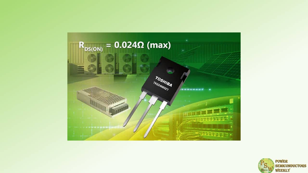
Toshiba Electronics Europe GmbH has launched an N-channel power MOSFET to address the growing market demand for improved efficiency in power supply circuits. The new TK024N60Z1 uses the proven DTMOSVI 600V series process with a super junction structure to achieve low on-resistance and reduced conduction losses. Applications include servers in data centres, switched-mode power supplies for industrial equipment, and power conditioners for photovoltaic generators.
The TK024N60Z1 has a drain-source on-resistance RDS(ON) of 0.024Ω (max), which is the lowest in the DTMOSVI 600V series. It also improves power supply efficiency, which reduces heat generation. Combined with the TO-247 package, which delivers high heat dissipation, the TK024N60Z1 offers good heat management characteristics.
Like other MOSFETS in the DTMOSVI 600V series, the TK024N60Z1 benefits from an optimised gate design and process. This reduces the value of drain-source on-resistance per unit area by approximately 13%. More importantly, drain-source on-resistance × gate-drain charge is reduced by approximately 52% compared to Toshiba’s conventional generation DTMOSIV-H series products with the same drain-source voltage rating. This means the DTMOSVI series, including the TK024N60Z1, offers a better trade-off between conduction loss and switching loss, which helps improve the efficiency of switched-mode power supplies.
To further improve power supply efficiency, Toshiba offers tools that support circuit design for switched-mode power supplies. These include the G0 SPICE model, which quickly verifies circuit function, and the highly accurate G2 SPICE models that reproduce transient characteristics.
The TK024N60Z1 N-channel power MOSFET exemplifies Toshiba’s commitment to continue expanding the DTMOSVI series and support energy conservation by reducing power loss in switched-mode power supplies.
Original – Toshiba
-

EPC is set to highlight cutting-edge advancements in AI, robotics, and other high-density power conversion applications at the Applied Power Electronics Conference (APEC) 2025. During the event, held from March 16 to March 20 in Atlanta, GA, EPC will focus on demonstrating how GaN is revolutionizing AI infrastructure, humanoid robotics, industrial and consumer applications in booth 1231.
AI = GaN: Enabling the Next Generation of AI Servers
Artificial intelligence requires ultra-efficient power conversion to sustain increasing computing densities. EPC’s latest GaN solutions for AC/DC server power and 48 V DC-DC GPU power reduce losses, increase power density, improve thermal management, and offer superior efficiency.
Motor Drives: Powering Robotics, Automation, and More
From industrial automation to consumer electronics, GaN-based motor drives offer higher efficiency, smaller size, and improved performance over traditional silicon-based solutions. EPC will showcase live demonstrations of GaN-powered drives in applications such as:
- Power tools – Enhanced battery life and performance with GaN motor drives
- Humanoids & quadrupeds – Next-generation robotics with faster response times and increased power efficiency
- Vacuum cleaners & delivery bots – Smarter, more autonomous systems benefiting from GaN’s high-speed switching and power density
Visit EPC at APEC 2025
- Schedule a Meeting: EPC’s technical experts, including CEO Dr. Alex Lidow, will be on-site to discuss how GaN is driving innovation across multiple industries. To schedule a meeting during APEC 2025 contact info@epc-co.com
- Exhibition Booth # 1231: Visit EPC’s booth to explore our comprehensive portfolio of GaN-based solutions. See firsthand the superior performance in live demonstrations
- Technical Presentations: Attend our technical sessions to gain insights into the latest trends and advancements in GaN power conversion technology
- Enhance Traction Motor Efficiency using a GaN based Four-Level Flying Capacitors Inverter
Industry Session (IS03.3): March 18 at 9:20 a.m.
Speaker: Marco Palma - Debate Session 1: SiC vs GaN – Which will lead in power conversion?
March 18 at 4:30 p.m.
Panelist: Alex Lidow, Ph.D. - High performance 5 kW, 4-Level totem-pole PFC converter using 200 V GaN FETs for open compute servers
Industry Session (IS12.2): March 19 at 8:55 a.m.
Speaker: Michael de Rooij, Ph.D. - Powerstage GaN Integrated Circuits Operation in Robotic Applications
Industry Session (IS14.4): March 19 at 2:45 p.m.
Speaker: Marco Palma
- Enhance Traction Motor Efficiency using a GaN based Four-Level Flying Capacitors Inverter
At APEC 2025, we are excited to showcase how EPC’s GaN solutions are setting new benchmarks in power conversion and efficiency,
said Nick Cataldo, VP of Sales and Marketing at EPC.Original – Efficient Power Conversion
-

Navitas Semiconductor announced unaudited financial results for the fourth quarter and full year ended December 31, 2024.
“I am proud of our team’s efforts to deliver growth in 2024, despite significant headwinds with an industry-wide slow-down in some major markets,” said Gene Sheridan, CEO and co-founder. “We achieved record GaN revenues from mobile, consumer and appliance sectors, while both GaN and SiC started shipping into data centers in the second half of 2024. We closed the year with an extraordinary $450 million of customer design-wins, which gives us increased confidence to resume a healthier growth rate in late ‘25 and beyond and continue to grow significantly faster than the overall power semiconductor market.”
4Q24 Financial Highlights
- Revenue: Total revenue was $18.0 million in the fourth quarter of 2024, compared to $26.1 million in the fourth quarter of 2023 and compared to $21.7 million in the third quarter of 2024.
- Loss from Operations: GAAP loss from operations for the quarter was $39.0 million, compared to a loss of $26.8 million for the fourth quarter of 2023 and a loss of $29.0 million for the third quarter of 2024. On a non-GAAP basis, loss from operations for the quarter was $12.7 million compared to a loss of $9.7 million for the fourth quarter of 2023 and a loss of $12.7 million in the third quarter of 2024.
- Cash: Cash and cash equivalents were $86.7 million as of December 31, 2024.
FY 2024 Financial Highlights
- Revenue: Total revenue grew to $83.3 million in 2024, a 5% increase from $79.5 million in 2023.
- Loss from Operations: GAAP loss from operations for the year was $130.7 million, compared to a loss of $118.1 million for 2023. On a non-GAAP basis, loss from operations for the year was $49.7 million compared to a loss of $40.3 million for 2023.
Market, Customer and Technology Highlights:
- Customer pipeline: increased 92% from $1.25 billion in December 2023, to $2.4 billion in December 2024.
- Data Center: AI driving fastest-growing end-market within customer pipeline, now valued at $165 million, up more than 100% vs. 2023; Navitas-designed 2.7 kW to 8.5 kW system platforms fueling 40 customer wins in 2024 with GaN and SiC AC-DC power supplies; now expanding into 48 V DC-DC converters with new 80-120 V GaN technology.
- EV: Over 40 customer wins in 2024 from US, Europe, Korea and China regions primarily with SiC in onboard and roadside chargers; first GaN EV win announced for 2026 production – extending driving range and reducing charging costs vs. traditional silicon on-board chargers.
- Mobile: Over 180 customer wins in 2024; continue to supply 10 of top 10 smartphone / notebook OEMs with Navitas GaN ICs; GaN reaches 10% adoption globally vs. silicon in mobile chargers and expands reach into Middle East, Africa, Latin America and India.
- Solar/Appliance/Industrial: On-track for GaN solar micro-inverter launch this summer expected to improve solar energy efficiencies, weight, size and cost; over 170 customer wins across solar, appliance and industrial.
Technology Announcement (March 12th live-stream event):
- Navitas will unveil a breakthrough in power conversion that will create a paradigm shift across multiple, major end markets. This includes both semiconductor and system-level innovations, and is expected to drive major improvements in energy efficiency and power density, further accelerating GaN and SiC adoption vs. legacy silicon devices. For more details, refer to: https://navitassemi.com/navitas-to-unveil-a-new-paradigm-in-power/.
Business Outlook
- First quarter 2025 net revenues are expected to be $13.0 to $15.0 million. Non-GAAP gross margin for the first quarter is expected to be 38% plus or minus 50 basis points, and non-GAAP operating expenses are expected to be approximately $18.0 million in the first quarter of 2025.
Original – Navitas Semiconductor
-

Manufacturers of cutting-edge audio equipment constantly seek to enhance sound quality while also meeting the growing demand for compact, lightweight, more integrated, and energy-efficient designs. At the same time, they must ensure seamless connectivity, cost-effectiveness, and user-friendly functionality, making audio product development more complex than ever.
To overcome these challenges, SounDigital has integrated CoolGaN™ transistors from Infineon Technologies AG into its new 1500 W Class D amplifier, featuring an 800 kHz switching frequency and five channels. Infineon’s advanced GaN technology has improved the energy efficiency of the amplifier by five percent and reduced energy loss by 60 percent.
“We are excited to enhance the performance of our audio amplifiers using Infineon’s GaN power semiconductors, enabling us to inspire people and provide entertainment by amplifying music around the world,” said Juliano Anflor, CEO of SounDigital. “GaN transistors significantly enhances our overall system performance with minimized system cost and increased ease of use.”
“GaN technology is transforming the audio amplifier industry, providing unparalleled efficiency and performance,” said Johannes Schoiswohl, Head of the GaN Business Line at Infineon. “Infineon’s leading GaN solutions deliver superior sound quality, higher power density, and reduced energy consumption, enabling SounDigital’s audio systems to reach new levels of fidelity and performance.”
For its 1500 W Class D amplifier, SounDigital selected Infineon’s 100 V normally-off E-mode transistors: IGC033S101 in a PQFN-3×5 package and IGB110S101 in a PQFN-3×3 package. With their low on-resistance, the transistors are ideal for demanding high-current applications, enabling significant improvements in both sound quality and efficiency of SounDigital’s amplifier.
The GaN-based amplifier also delivers high performance while reducing power dissipation by 75 W, allowing for a 50 percent smaller heat sink. Additionally, the overall system size has been reduced by 40 percent without compromising performance. The audio quality has been further improved by the CoolGaN transistors, with total harmonic distortion (THD) reduced by 70 percent, enabling a more precise and detailed sound experience. At the same time, the idle current has been reduced by 40 percent, significantly improving energy efficiency.
Original – Infineon Technologies
-

Navitas Semiconductor has announced it will attend APEC 2025 and highlight the latest advances in GaN and SiC wide bandgap technologies for AI data center EV, and mobile applications. Additionally, Navitas will highlight its latest ‘paradigm in power conversion’, unveiled in a live-streamed press event on the 12th of March.
APEC takes place at Atlanta’s Georgia World Congress Center from March 16th to 20th. The company’s “Planet Navitas” stand (Booth #1107) will showcase the company’s mission to ‘Electrify our World™’ by advancing the transition from legacy silicon to next-generation, clean energy GaN and SiC power semiconductors. These technologies are designed for high-growth markets that demand the highest efficiency and power density. The shift from silicon to GaN and SiC technologies has the potential to save over 6,000 megatons of CO2 per year by 2050. Recent Navitas breakthroughs that will be highlighted on the stand include:
- Navitas’ breakthrough that will create a paradigm shift in power conversion – full details will be unveiled in a live-streamed press event on the 12th of March.
- World’s First 8.5 kW AI Data Center Power Supply: See the world’s first 8.5 kW OCP power solution achieving 98% efficiency for AI and hyperscale data centers. Featuring high-power GaNSafe™ power ICs and Gen-3 Fast SiC MOSFETs in 3-Phase Interleaved CCM Totem-Pole PFC and 3-Phase LLC topologies to provide the highest efficiency, performance, and lowest component count.
- World’s Highest Power Density AI Power Supply: Navitas delivers efficient 4.5 kW power in the smallest power-supply form-factor for the latest AI GPUs that demand 3x more power per rack. The optimized design uses high-power GaNSafe ICs and Gen-3 Fast SiC MOSFETs enabling the world’s highest power density with 137 W/in3 and over 97% efficiency.
- ‘IntelliWeave’ Patented Digital Control Optimized for AI Data Center Power Supplies: Combined with high-power GaNSafe™ and Gen-3 ‘Fast’ SiC MOSFETs to enable PFC peak efficiencies of 99.3% and reduce power losses by 30% compared to existing solutions.
- Mid-voltage GaNFast FETs targeting 48V AI data center power supplies, next-generation EV platforms EV and AI-based robotics, to enable high-frequency, high-efficiency, and high-power density power conversion systems.
- GaNSlim™: Simple. Fast. Integrated: A new generation of highly integrated GaN power ICs that will further simplify and speed the development of small form factor, high-power-density applications by offering the highest level of integration and thermal performance. Target applications include chargers for mobile devices and laptops, TV power supplies, and lighting systems of up to 500W.
- Automotive Qualified (AEC-Q101) Gen-3 Fast SiC MOSFETs with ‘trench-assisted planar’ technology: Enabled by over 20 years of SiC innovation leadership, GeneSiC™ technology leads on performance with the Gen-3 ‘Fast’ SiC MOSFETs with ‘trench-assisted planar’ technology. This proprietary technology provides world-leading performance over temperature, delivering cool-running, fast-switching, and superior robustness to support faster charging EVs and up to 3x more powerful AI data centers.
- SiCPAK™ High-Power Modules – Built for Endurance and Performance: Utilizing industry-leading ‘trench-assisted planar’-gate technology and epoxy-resin potting for increased power cycling and long-lasting reliability, SiCPAK modules offer compact form factors and provide cost-effective, power-dense solutions for applications including EV charging, drives, solar, and energy storage systems (ESS).
- New Advancements in our Leading GaNFast & GeneSiC technology:
- GeneSiC MOSFETs specifically optimized for EV traction modules with additional screening and gold metallization for sintering.
- GaNSense™ motor drive ICs with bi-directional loss-less current sensing, voltage sensing, and temperature protection, further enhancing performance and robustness beyond what is achievable by any discrete GaN or discrete silicon device.
Navitas will participate and present in the Industry Session which showcases the latest work in all areas of power electronics.
Technical Presentations:
Wednesday 19th March
- ‘GaNSlim Power IC & DPAK-4L Package Enables 100W, 100cc, PD3.1 Continuous Power Solution with 95% Efficiency’
- 2:20 pm, IS14.3, A411, Tom Ribarich, Sr Dir. Strategic Marketing
- ‘500kHz Inverter Design Using Bidirectional GaN Switches’
- 8:30 am, IS11.1, A403, Jason Zhang, VP Applications & Technical Marketing
- ‘Advancing Power Solutions: Integrating Wide Bandgap Technologies for Next-Generation Applications’
- 1:30 pm – 4:55 pm ET, IS14, Llew Vaughan-Edmunds, Session Chair.
- ‘WBG Converter Design’
- 8:30 am – 11:55 am ET, IS11.1, Jason Zhang, Session Chair.
Thursday 20th March
- ‘Marketing & Technology Trends in Power Electronics’
- 10:10 AM – 11:50 AM ET, Stephen Oliver, Session Chair.
Original – Navitas Semiconductor
