-

Navitas Semiconductor is set to unveil a breakthrough in power conversion that will create a paradigm shift across multiple major end markets. These developments include both semiconductor and system innovations which are expected to drive major improvements in energy efficiency & power density and further accelerate the adoption of gallium nitride and silicon carbide technologies to displace silicon.
The live-streamed event will take place on March 12th at 8 am PST and will be re-streamed (in both Chinese and English) at 6 pm PST.
Co-founders, Gene Sheridan (CEO), Dan Kinzer (CTO, COO) and Jason Zhang (VP Engineering) will uncover this next inflection in power conversion, including technology details, specific application examples and describe the expected market impacts & business opportunities from these innovations.
- Register now, 8 am Pacific: https://bit.ly/NavitasLiveEvent-8am-PT
- Register now, 6 pm Pacific: https://bit.ly/NavitasLiveEvent-6pm-PT
Original – Navitas Semiconductor
-

Infineon Technologies AG has made significant progress on its 200 mm silicon carbide (SiC) roadmap. The company will already release the first products based on the advanced 200 mm SiC technology to customers in Q1 2025. The products, manufactured in Villach, Austria, provide first-class SiC power technology for high-voltage applications, including renewable energies, trains, and electric vehicles. Additionally, the transition of Infineon’s manufacturing site in Kulim, Malaysia, from 150-millimeter wafers to the larger and more efficient 200-millimeter diameter wafers is fully on track. The newly built Module 3 is poised to commence high-volume production aligned with market demand.
“The implementation of our SiC production is progressing as planned and we are proud of the first product releases to customers,” said Dr. Rutger Wijburg, Chief Operations Officer of Infineon. “By ramping up SiC production in Villach and Kulim in phases, we are improving cost-efficiency and continuing to ensure product quality. At the same time, we are making sure our manufacturing capacities can meet the demand for SiC-based power semiconductors.”
SiC semiconductors have revolutionized high-power applications by switching electricity even more efficiently, demonstrating high reliability and robustness under extreme conditions, and by making even smaller designs possible. Infineon’s SiC products let customers develop energy-efficient solutions for electric vehicles, fast charging stations and trains as well as renewable energy systems and AI data centers.
The release to customers of the first SiC products based on the 200-millimeter wafer technology marks a substantial step forward in Infineon’s SiC roadmap, with a strong focus on providing customers with a comprehensive portfolio of high-performance power semiconductors that promote green energy and contribute to CO 2 reduction.
As “Infineon One Virtual Fab” for highly innovative wide-bandgap (WBG) technologies, Infineon’s production sites in Villach and Kulim share technologies and processes which allow for fast ramping and smooth and highly efficient operations in SiC and gallium nitride (GaN) manufacturing. The 200-millimeter SiC manufacturing activities now add to Infineon’s strong track record of delivering industry-leading semiconductor technology and power system solutions and strengthen the company’s technology leadership across the entire spectrum of power semiconductors, in silicon as well as in SiC and GaN.
Original – Infineon Technologies
-

The electronics industry is experiencing a significant shift towards more compact and powerful systems. To support this trend and further drive innovation at the system level, Infineon Technologies AG is expanding its portfolio of discrete CoolSiC™ MOSFETs 650 V with two new product families housed in Q-DPAK and TOLL packages.
These diverse product families, with top- and bottom-side cooling, are based on the CoolSiC™ Generation 2 (G2) technology and offer significantly improved performance, reliability, and ease of use. The product families target high- and medium-power switched-mode power supplies (SMPS) including AI servers, renewable energy, chargers for electric vehicles, e-mobility and humanoid robots, televisions, drives and solid-state circuit breakers.
The TOLL package offers outstanding Thermal Cycling on Board (TCoB) capability, enabling compact system designs by reducing the printed circuit board (PCB) footprint. When used in SMPS, it can also reduce system-level manufacturing costs. The TOLL package now fits an extended list of target applications, enabling PCB designers to further reduce costs and better meet market demands.
The introduction of the Q-DPAK package complements the ongoing development of Infineon’s new family of Topside Cooled (TSC) products, which includes CoolMOS™ 8, CoolSiC™, CoolGaN™ and OptiMOS™. The TSC family enables customers to achieve excellent robustness with maximum power density and system efficiency at low cost. It also enables direct heat dissipation of 95 percent, allowing the use of both sides of the PCB for better space management and reduction of parasitic effects.
The CoolSiC™ MOSFETs 650 V G2 in TOLL are now available in R DS(on) from 10 to 60 mΩ, while the Q-DPAK variant is available in 7, 10, 15 and 20 mΩ.
Original – Infineon Technologies
-

GlobalFoundries Inc. (GF) announced preliminary financial results for the fourth quarter and fiscal year ended December 31, 2024.
Key Fourth Quarter Financial Highlights
- Revenue of $1.830 billion
- Gross margin of 24.5% and Non-IFRS gross margin of 25.4%
- Operating margin of (38.3)% and Non-IFRS operating margin of 15.6%
- Net loss of $729 million and Non-IFRS net income of $256 million
- Diluted loss per share of $1.32 and Non-IFRS diluted earnings per share of $0.46
- Non-IFRS adjusted EBITDA of $661 million
- Ending cash, cash equivalents and marketable securities of $4.2 billion
- Net cash provided by operating activities of $457 million and Non-IFRS adjusted free cash flow of $328 million
Key Full Year 2024 Financial Highlights
- Revenue of $6.750 billion
- Gross margin of 24.5% and Non-IFRS gross margin of 25.3%
- Net loss of $262 million and Non-IFRS net income $870 million
- Diluted loss per share of $0.48 and Non-IFRS diluted earnings per share of $1.56
- Non-IFRS adjusted EBITDA of $2.475 billion
- Year to date net cash provided by operating activities of $1.722 billion and Non-IFRS adjusted free cash flow of $1.107 billion
“In the fourth quarter, the GF team delivered solid financial results that exceeded the Non-IFRS midpoint of the guidance ranges we provided in our November earnings release,” said Dr. Thomas Caulfield, President and CEO of GF. “2024 presented a unique set of challenges for our industry, but thanks to our focus on operational excellence, we generated over $1 billion of Non-IFRS adjusted free cash flow. As we look to 2025, we are encouraged by our strong design win momentum across our end markets and product portfolio as we position GF for a growth year.”
In the fourth quarter 2024, GF recorded a $935 million impairment charge on the long-lived assets relating to legacy investments in production capacity at its facility in Malta, New York. GF undertook this action pursuant to the diversification of its long-term manufacturing technology platform roadmap in Malta, which is consistent with the Company’s previously communicated technology transfer strategy needed to meet expected long-term customer demand. Since such impairment is not expected to be a recurring event, the Company believes this additional adjustment to Non-IFRS metrics better enables management and investors to make more meaningful comparisons of fourth quarter 2024 results against prior periods.
Recent Business Highlights
- GF announced a first-of-its-kind center for advanced packaging and test capabilities, to be developed at its Malta, New York facility. Supported by grants from New York State and the U.S. Department of Commerce, GF’s Advanced Packaging and Photonics Center will help meet the growing demand for U.S.-made essential chips used in AI, automotive, aerospace and defense, and communications applications.
- IDEMIA and GF announced a partnership to deliver next-generation smart card technology with improved data retention, low read latency and enhanced power efficiency – saving customers cost and time. This multi-year collaboration will be 100% manufactured and tested in Europe on GF’s 28ESF3 platform, ensuring trusted providence.
- Lightmatter announced that it will use GF’s Fotonix™ fabrication platform to develop the industry’s most robust and scalable AI interconnect solution. By integrating electronics and photonics into a single CMOS wafer, GF’s unique solution will enable the speed and efficiency needed for future AI data centers.
Original – GlobalFoundries
-

Axcelis Technologies, Inc. announced financial results for the fourth quarter and full year ended December 31, 2024.
For the full year 2024, the Company reported revenue of $1.02 billion, compared with $1.13 billion for the full year 2023. Systems revenue for the year was $782.6 million, compared to $883.6 million in 2023. Operating profit was $210.8 million in 2024, compared to $265.8 million in 2023. Net income for the year was $201 million with diluted earnings per share of $6.15, compared to net income of $246.3 million and diluted earnings per share of $7.43 in 2023. Gross margin for the year was 44.7%, compared to 43.5% in 2023.
The Company reported fourth quarter revenue of $252.4 million, compared to $256.6 million for the third quarter of 2024. Gross margin for the quarter was 46.0%, compared to 42.9% in the third quarter. Operating profit for the quarter was $54.5 million, compared to $46.9 million for the third quarter. Net income for the quarter was $50 million, or $1.54 per diluted share, compared to $48.6 million, or $1.49 per diluted share in the third quarter.
President and CEO Russell Low commented, “Axcelis exited the year on a strong note, with fourth quarter revenue and profitability exceeding our expectations. As we look ahead to 2025, we anticipate a near term cyclical digestion period, as customers absorb the robust investments they’ve made into mature node capacity over the past few years – particularly in China. We are focused on capturing the long-term growth opportunities that lie ahead by investing in product innovation, managing our costs, and working closely with customers on their technology roadmaps – all of which will put us in an even stronger position for the next upturn.”
Executive Vice President and Chief Financial Officer Jamie Coogan said, “We are pleased with our financial execution in 2024. Despite a decline in revenue, we were able to deliver higher gross margins, generate solid free cash flow, return capital to shareholders via buyback, and exit the year with a stronger balance sheet that allows us to invest during this cyclical digestion period and drive long term value creation.”
For the first quarter ending March 31, 2025, Axcelis expects revenues of approximately $185 million, and earnings per diluted share of approximately $0.38.
Original – Axcelis Technologies
-

Efficient Power Conversion Corporation (EPC) announced the release of the 4th edition of its groundbreaking textbook, GaN Power Devices for Efficient Power Conversion.
This latest edition reflects the rapid advancements in GaN technology and its transformative impact across various industries, including renewable energy, electric vehicles, data centers, robotics, and space applications. Co-authored by EPC CEO Dr. Alex Lidow and a team of GaN experts, the textbook remains an indispensable resource for engineers, students, and industry innovators looking to stay at the forefront of power electronics.
What’s New in the 4th Edition
- Expanded coverage on the integration of GaN into new applications such as AI servers, autonomous systems, and eMobility
- Updates on design techniques that maximize GaN’s superior efficiency, power density, and thermal performance
- Comprehensive insights into GaN ICs and their role in simplifying complex designs and improving system reliability
- A dedicated section on the latest advancements in GaN reliability and manufacturability
- Real-world application examples, case studies, and practical design tips for engineers.
“Since its inception, this textbook has guided engineers and innovators adopting GaN,” said Dr. Alex Lidow, CEO and co-author. “The 4th edition deepens understanding of GaN’s capabilities and empowers readers to unlock its full potential.”
This edition underscores EPC’s commitment to educating the power electronics community and supporting the adoption of GaN as the go-to technology for efficient power conversion. The textbook is available for purchase through Wiley.
Availability and Additional Resources
The 4th edition of GaN Power Devices for Efficient Power Conversion is available now. For additional resources, including evaluation boards, design support tools, and application notes, visit epc-co.com.
Original – Efficient Power Conversion
-
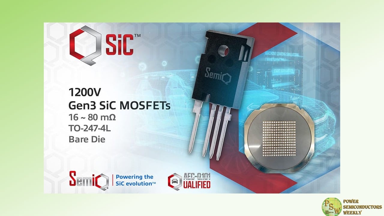
SemiQ Inc has announced the QSiC 1200V MOSFET, a third-generation SiC device that shrinks the die size while improving switching speeds and efficiency.
The device is 20% smaller versus QSiC’s second-generation SiC MOSFETs and has been developed to increase performance and cut switching losses in high-voltage applications. SemiQ is targeting a diverse range of markets including EV‑charging stations, solar inverters, industrial power supplies and induction heating.
It will be on display for the first time at the Applied Power Electronics Conference (APEC), on March 16-20, 2025.
In addition to having a drain-to-source voltage (VDS) of 1200 V, the MOSFET reduces total switching losses to 1646 µJ and has a low on-resistance (RDS,on) of 16.1 mΩ. It is available as a bare die or in a four-pin TO-247 4L discrete package measuring 31.4 x 16.1 x 4.8 mm, which includes a reliable body diode and a driver-source pin for gate driving.
High-quality Known Good Die (KGD) testing has been conducted using UV tape and Tape & Reels, with all parts undergoing testing and verification at voltages exceeding 1400V, as well as being avalanche tested to 800 mJ. Reliability is further improved through the device’s 100% wafer-level gate oxide burn-in screening and 100% UIL testing of discrete packaged devices.
The device has been developed to have a low reverse recovery charge (QRR 470 nC) and lower capacitance, improving switching speed, switching losses, EMI and overall efficiency; to be easy to parallel; and with a longer creepage distance (9 mm), improving electrical insulation, voltage tolerance and reliability.
Dr. Timothy Han, President at SemiQ said: “The move to Gen3 SiC further increases the benefits of SiC MOSFETs over IGBTs. These devices not only deliver vastly improved performance, but cut die size and cost versus previous generations. As a result, the launch of the QSiC 1200V opens the technology, and its benefits, to a far greater range of applications. The device delivers industry leading performance figures, notably on gate threshold voltage, and we’re delighted to be demonstrating this first at APEC.”
The QSiC 1200V MOSFETs has a continuous operational and storage temperature of -55oC to 175oC. It has a recommended operational gate-source voltage of -4/18 V, with a VGSmax of -8/22 V, and a power dissipation of 484 W (core and junction temperature 25oC).
For static electrical characteristics, the device has a junction-to-case thermal resistance of 0.26oC per watt (40oC per watt junction to ambient). Its Zero gate voltage drain current is 100 nA, with a gate-source voltage current of 10 nA. Its AC characteristics include a turn-on delay time of 21 ns with rise time of 25 ns; its turn-off delay time is 65 ns with a fall time of 20 ns.
An increased range of resistances is available in bare-die and TO-247 4L packages with the following options:
- 16 mΩ: GP3T016A120X / GP3T016A120H
- 20 mΩ: GP3T020A120X / GP3T020A120H
- 40 mΩ: GP3T040A120X / GP3T040A120H
- 80 mΩ: GP3T080A120X / GP3T040A120H
Both the 16 mΩ (AS3T016A120X / AS3T016A120H) and 40 mΩ (AS3T040A120X / AS3T040A120H) options have been qualified for Automotive Applications Product Validation according to AEC-Q101.
The SemiQ QSiC 1200V will be on display at the Georgia World Congress Center in Atlanta, from March 16 to 20, 2025. Visitors to SemiQ’s booth #1348 will have the opportunity to explore the new third-generation MOSFETs.
Original – SemiQ
-

Cambridge GaN Devices (CGD) has announced that Henryk Dabrowski, appointed as SVP of Global Sales at the innovative GaN IC company last year, will lead CGD’s global sales strategy, building on the successes to date, by expanding into additional markets exploiting the significant advantages that ICeGaN® offers. As part of that expansion, CGD is growing its sales organisation and will be hiring regional sales managers for both EMEA and North America, who will report to Dabrowski.
HENRYK DABROWSKI | SVP OF GLOBAL SALES, CGD
“GaN is now generally acknowledged to be a disruptive power semiconductor technology with an established growth trajectory, enabling high efficiency, high power density and miniaturisation. It is a perfect opportunity for CGD, which has demonstrated the ruggedness, reliability and ease of use of its ICeGaN® GaN IC technology. I am, therefore, delighted to be leading the sales focus as we scale up with major global customers in applications including servers, data centres, inverters, industrial power supplies and, in the near future, automotive EV applications.”GIORGIA LONGOBARDI | CEO & CO-FOUNDER, CGD
“I am thrilled to have Henryk onboard. His extensive industry expertise, strategic vision and proven success will enable CGD’s rapid expansion into new markets world-wide. As the demand for power significantly increases due to AI and the electrification of vehicles, I am confident that Henryk’s expertise will be key to accelerating commercial adoption of CGD’s effortless and energy-efficient ICeGaN® GaN ICs.”Dabrowski has over 30 years’ experience in technology design, commerce and sales leadership. Most recently, he built and led sales and applications teams for Vicor in EMEA. A Chartered Engineer (CEng) with the Institute of Engineering and Technology (IET), Dabrowski previously held commercial roles at Texas Instruments and Infineon, and also has experience within the distribution sales channel.
Original – Cambridge GaN Devices
-

Navitas Semiconductor’s 8.5kW power supply unit (PSU), powered by GaNFast™ and GeneSiC™ technologies, has been recognized for its innovative design. Tailored for AI and hyperscale data centers, the PSU achieves 98% efficiency while meeting Open Compute Project (OCP) and Open Rack v3 (ORv3) specifications.
The design minimizes ripple current, EMI, and device count by 25%, reducing costs. Its 3-phase LLC topology utilizes GaNSafe™ technology with integrated control, drive, sensing, and protection, along with Gen-3 Fast SiC MOSFETs for enhanced performance and reliability.
Original – Navitas Semiconductor
-

SUMCO Corporation announced plans to transfer wafer production from the Miyazaki Plant of consolidated subsidiary SUMCO TECHXIV Corporation to other manufacturing facilities, with the aim of improving profitability by reorganizing the production of silicon wafers of 200 mm and smaller.
The current silicon wafer market environment is in a prolonged sluggish demand phase, due to such factors as the drop-off from extraordinary demand during the COVID-19 pandemic, and structural changes in the semiconductor supply chain occasioned by US-China friction.
Drawdown of 300 mm wafer inventories by customers is taking time, as semiconductor production adjustments continue; but overall demand is expected to recover gradually thanks to strong needs for leadingedge products for AI semiconductors and high-performance memory. Demand remains sluggish, however, for small-diameter wafers mainly for consumer, industrial, and automotive uses. Wafers of 150 mm and smaller, in particular, are expected to see falling demand, with customers shifting to 200 mm wafers or lowering their production capacity as manufacturing equipment reaches its end of life.
In this market environment, the SUMCO Group has decided to reorganize the Miyazaki Plant to improve efficiency through consolidation of the production capacity of small wafers. The Miyazaki Plant will become a factory solely for monocrystalline production, while wafer production will be transferred to other domestic plants in the SUMCO Group and to Indonesia, ending wafer production in Miyazaki by the end of 2026.
SUMCO intends to reassign employees affected by the reorganization to 300 mm wafer operations after the end of wafer production in Miyazaki. With this reorganization, expenses for business structural reforms have been posted for fiscal 2024 as extraordinary losses totaling 5.8 billion yen, consisting of an impairment loss on non-current assets of 4.6 billion yen and an inventory write-down, etc., of 1.2 billion yen.
The SUMCO Group is committed to ongoing efficiency-raising initiatives, including reorganization of production facilities. Moreover, with the accelerating pace of innovation in semiconductor technology, in addition to strategically making use of advanced manufacturing equipment currently under preparation for operation, we will focus management resources on modernizing equipment in existing 300 mm plants and boost our capacity for supplying leading-edge products for AI with their remarkable growth, as we strive to further raise our corporate value.
Original – SUMCO
