-

Axcelis Technologies, Inc. will be the Diamond Sponsor for the Compound Semiconductor Asia Conference (CS Asia) 2025. The event is being held in conjunction with SEMICON China 2025 on March 25-27, 2025, at the Kerry Hotel in Pudong, Shanghai. Axcelis’ President and CEO, Russell Low, will present an opening Keynote Speech at the event.
Innovation in Ion Implantation for Power and Compound Semiconductor Devices
Russell Low, PhD
President & CEO, Axcelis Technologies
14:30 – 15:00
Shanghai Ballroom 3, Kerry HotelPresident and CEO Russell Low, said, “We’re pleased to be a part of SEMICON China and especially excited about participating in the CS Asia Conference, one of the most important power and compound semiconductor technology forums in the Asia Pacific region. Axcelis is well positioned with a broad portfolio and deep technical expertise in this market, and we look forward to providing our innovative ion implant technology to chipmakers in China.”
Original – Axcelis Technologies
-

Many industrial applications today are moving towards higher power levels with minimized power losses. One way to achieve this is to increase the DC link voltage. Infineon Technologies AG is addressing this market trend with the CoolSiC™ Schottky diode 2000 V G5 product family, the first discrete silicon carbide diodes with a breakdown voltage of 2000 V, introduced in September 2024.
The product portfolio has now been expanded to include a Schottky diode in the TO-247-2 package, which is pin-compatible with most existing TO-247-2 packages. The product family fits perfectly for applications with DC link voltages up to 1500 V DC, making it ideal for solar and EV chargers.
The CoolSiC Schottky diode 2000 V G5 in the TO-247-2 package is available with current ratings ranging from 10 to 80 A. It allows developers to achieve higher power levels in their applications while reducing the component count by half compared to 1200 V solutions. This simplifies the overall design and facilitates a seamless transition from multi-level to two-level topologies.
In addition, the Schottky diode in the TO-247-2 package incorporates .XT interconnection technology, which significantly reduces thermal resistance and impedance, thereby enhancing heat management. Humidity robustness has been validated through HV-H3TRB reliability testing. The diodes exhibit neither reverse recovery nor forward recovery, and feature a low forward voltage, ensuring improved system performance.
The 2000 V diode family is a perfect match for the CoolSiC MOSFETs 2000 V in the TO-247Plus-4 HCC package that Infineon launched in the spring of 2024. In addition to the TO-247-2 package, the CoolSiC Schottky Diode 2000 V is also available in the TO-247PLUS-4 HCC package.
Original – Infineon Technologies
-
NoMIS Power has announced a major breakthrough in improving the short-circuit withstand time (SCWT) of SiC MOSFETs. This innovation addresses one of the key challenges limiting the widespread adoption of SiC technology in high-power applications.
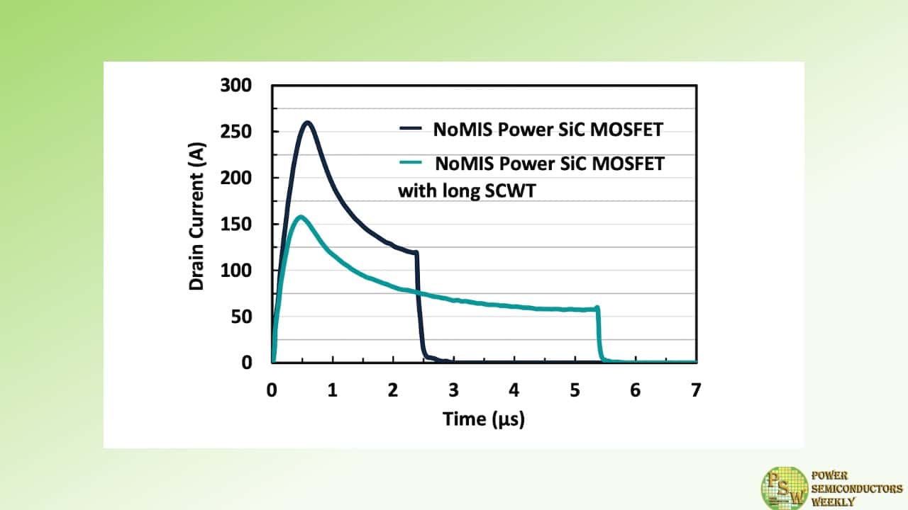
Silicon carbide (SiC) devices have gained prominence in power electronics due to their high efficiency, fast switching, and superior thermal performance. However, their historically lower short-circuit robustness compared to silicon-based IGBTs has posed challenges for their use in high-voltage and high-reliability environments, such as industrial drives, electric vehicles, and grid applications. NoMIS Power’s latest advancement significantly extends the SCWT of SiC MOSFETs to a minimum of 5 µs (Fig. 1), compared to the current industry standard of 2-3 µs, with no deleterious effect on specific on-resistance (Ron,sp) (Fig. 2). This enhancement greatly improves reliability and unlocks new opportunities for system designers seeking to maximize performance while maintaining fault tolerance.
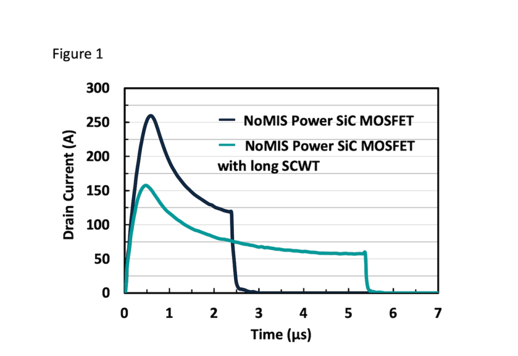
Figure 1: Drain currents of the NoMIS Power SiC MOSFET and NoMIS Power SiC MOSFET with long SCWT under short-circuit conditions right before failure. Drain currents of the 1.2 kV, 80 mΩ SiC MOSFET (dark blue) and the long SCWT 1.2 kV, 80 mΩ SiC MOSFET (light blue) from NoMIS Power are compared. The measurement for short-circuit was conducted under the following conditions: Rg of 20 Ω, Vgs of 20 V, and a Vds of 800 V.
By tuning the trade-off between Ron,sp and SCWT using NoMIS Power’s proprietary SiC MOSFET fabrication design and process flow, the performance shown in Fig. 1 & Fig. 2 was achieved; and can be similarly managed depending on the specific application. Complete optimization of SiC MOSFETs with long SCWT using this approach will allow NoMIS Power to further extend the SCWT while maintaining negligible impact on Ron,sp.
Figure 2: Typical output characteristics of NoMIS Power 1.2 kV, 80 mQ SiC MOSFET and NoMIS Power 1.2 kV, 80 mQ SiC MOSFET with long SCWT showing no significant negative impact on on-resistance.
“At NoMIS Power, we have focused extensively on device architecture engineering, leading to a significant advancement in SiC short-circuit withstand time,” said Woongje Sung, CTO at NoMIS Power. “We believe this achievement provides valuable advantages to the power electronics community, helping engineers integrate SiC solutions with greater confidence in applications where robustness is critical.”
NoMIS Power’s long SCWT devices are well-screened for latent defects and offer easier gate driver desaturation (dSat) design for high di/dt and dv/dt, enabling faster switching frequencies of up to hundreds of kHz. Initial test results demonstrate a 2X to 4X increase in short-circuit withstand time compared to existing SiC devices, positioning NoMIS Power’s technology as a frontrunner in the next generation of power semiconductors. Additionally, when coupled with packaging innovations that impact junction-to-case thermal capacitance, alongside novel thermal management techniques with high heat transfer coefficients, the overall SCWT of the SiC MOSFET can be further improved.
The impact of this innovation extends across multiple industries, including renewable energy, electric transportation, and high-power industrial applications. A longer short-circuit withstand time ensures rugged and reliable performance in critical applications, reinforcing the robustness of SiC-based power systems. For example, built-in redundancy of the SiC MOSFETs inside power converters, which impacts costs as well as power density, can be reduced. Furthermore, applications sensitive to electromagnetic inference, that cannot solely rely on digital control and sensing schemes to detect and act upon short-circuit events, will now be able to effectively utilize SiC MOSFETs with lower risk. As SiC adoption accelerates, NoMIS Power’s breakthrough will play a pivotal role in enhancing the reliability and safety of SiC-based power converters and systems.
NoMIS Power is showcasing this breakthrough technology at APEC 2025, March 16-20, Atlanta, GA, Booth 548 along with its expanded range of SiC discretes and power modules.
Original – NoMIS Power
-

Magnachip Semiconductor Corporation announced financial results for the fourth quarter and full-year 2024.
Q4 Results Summary
- Consolidated revenue of $63 million was above the mid-point of our guidance range of $59.0 to $64.0 million.
- Standard Product business revenue was down 5.1% sequentially due primarily to seasonality.
- Consolidated gross profit margin of 25.2% was above the high-end our guidance range of 21.5% to 23.5%.
- Standard Product business gross profit margin was 26.6%, up 2.2 percentage points sequentially.
- Repurchased approximately 0.7 million shares for aggregate purchase price of $2.9 million during the quarter and ended Q4 with cash of $138.6 million.
2024 Highlights
- Excluding Transitional Foundry Services, Standard Products business revenue increased 13% year-over-year, with MSS up 22.5% and PAS up 10.2%. Both of these business line growth rates were in line with original guidance for double-digit growth provided at the beginning of 2024.
- PAS revenue growth was strongest in Communication, Computing and Consumer in calendar 2024. Automotive and Industrial declined only slightly, relatively outperforming the broader markets.
- Power IC revenue increased more than 50% year-over-year.
YJ Kim, Magnachip’s CEO, said, “Our Q4 revenue of $63 million was up 24% year-over-year, and gross profit margin of 25.2% was up 2.5 percentage points as compared to a year ago. For the year, Standard Products business revenue increased 13% year-over-year, in line with our guidance for double-digit growth that we provided at the beginning of 2024.”
YJ Kim added, “Our revenue and gross margin results represented a step in the right direction, but our utmost short-term goal is a return to profitability. To achieve this goal, Magnachip announced today its transition to become a pure-play Power company, and we also announced that we are exploring all strategic options for the Display business, which will be classified as discontinued operations when the Company reports Q1 results in May.”
YJ Kim commented, “By focusing on the Power business, Magnachip currently expects to achieve a quarterly Adjusted EBITDA breakeven by the end of Q4 2025 from continuing operations, followed by positive adjusted operating income in 2026, and positive adjusted free cash flow in 2027. Each of these targets will act as milestones towards achieving a goal in 3 years to reach a $300 million annual revenue run-rate with a 30% gross profit margin target. We call this our 3-3-3 strategy.”
Original – Magnachip Semiconductor
-

Navitas Semiconductor has announced a latest breakthrough of the world’s first production-released 650 V bi-directional GaNFast ICs and high-speed isolated gate-drivers, creating a paradigm shift in power with single-stage BDS converters, which enables the transition from two-stage to single-stage topologies. Targeted applications range widely and opens up multi-billion dollar market opportunities across EV charging (On-Board Chargers (OBC) and roadside), solar inverters, energy storage and motor drives. The recorded launch event video can be viewed here.
Over 70% of today’s high-voltage power converters use a ‘two-stage’ topology. For example, a typical AC-DC EV OBC implements an initial power-factor-correction (PFC) stage and a follow-on DC-DC stage, with bulky ‘DC-link’ buffering capacitors. The resulting systems are large, lossy, and expensive. Bi-directional GaNFast consolidates the two stages into a single, high-speed, high-efficiency stage and in the process, eliminates the bulky capacitors and input inductors – the ultimate solution in EV OBCs.
A leading EV and solar micro-inverter manufacturer have already begun their implementation of single-stage BDS converters to improve efficiency, size, and cost in their systems. GaNFast-enabled single-stage converters achieve up to 10% cost savings, 20% energy savings, and up to 50% size reductions.
The ultimate power semiconductor switch (transistor) can block voltage and allow current flow in two directions, with the highest efficiency. Navitas’ leadership in GaN innovation has delivered this landmark – the bi-directional GaNFast power IC.
Previously, two discrete, ‘back-to-back’ single switches had to be used, but new bi-directional GaNFast ICs are leading-edge, single-chip designs (monolithic integration) with a merged drain structure, two gate controls, and a patented, integrated, active substrate clamp. One high-speed, high-efficiency bi-directional GaNFast IC replaces up to 4 older switches, increasing system performance while reducing component count, PCB area, and system costs.
The initial 650 V bi-directional GaNFast ICs include NV6427 (100 mΩ RSS(ON) typ.) and NV6428 (50 mΩ RSS(ON) typ) in thermally enhanced, top-side-cooled TOLT-16L (Transistor Outline Leaded Topside-cooled) packaging. The product family will be extended into lower RSS(ON) offerings in the future.
The new, high-speed IsoFast devices are galvanically isolated, high-speed drivers optimized to drive bi-directional GaN. With 4x higher transient immunity than existing drivers (up to 200 V/ns) and no external negative bias supply needed, they deliver reliable, fast, accurate power control in high-voltage systems. Initial parts are the NV1702 (dual, independent-channel, digital, isolated bi-directional GaN gate driver) and NV1701 (half-bridge GaN digital isolator) in SOIC-16N and SOIC-14W packages.
“These ICs are a truly game-changing and disruptive technology both at the semiconductor and at the system level. They not only deliver improved efficiency, power density, simplicity, and system costs but will also transform multiple multi-billion-dollar markets in the most sustainable way possible.” Gene Sheridan, CEO and co-founder of Navitas commented. “The future of our electrified planet is bi-directional energy flow. From all renewable energy sources, the power grid, and all electrified applications, such as ESS, solar and EVs, energy should flow efficiently & bi-directionally, creating a critical new currency for our future planet. Single-stage BDS converters are the key for this inflection”.
Bi-directional GaNFast ICs (NV6427 and NV6428) are fully qualified and immediately available in mass-production quantities. IsoFast (NV1701 and NV1702) samples are available now to qualified customers.
Single-stage evaluation boards and user guide showcasing both IsoFast and bi-directional GaNFast ICs are available for qualified customers.
Navitas will feature bi-directional GaNFast ICs and IsoFast at the APEC 2025 power electronics conference in Atlanta, March 17th-19th, booth 1107.
Original – Navitas Semiconductor
-

Infineon Technologies AG has introduced its roadmap for next-level Battery Backup Unit (BBU) solutions for uninterrupted operations of AI data centers to avoid power outages and the risk of data losses. The comprehensive BBU roadmap includes power solutions from 4 kW up to the world’s first 12 kW battery backup unit. The BBU solutions are designed to deliver highly efficient, reliable, and scalable power conversion in AI server racks, and achieve a power density up to 400 percent higher compared to industry average.
BBUs are essential for AI data centers to provide an uninterruptible power supply and furthermore protect sensitive AI hardware from voltage spikes, surges, and other power anomalies by filtering and conditioning the power that is supplied to the data center equipment. Combined with various best-in-class topologies enabling an increased ease-of-use for customers, the BBU solutions are bolstering Infineon’s leading position in the field of powering artificial intelligence.
“Ensuring an uninterrupted power supply to AI systems is critical for maintaining process continuity and seamless operation,” said Adam White, Division President Power & Sensor Systems at Infineon. “Our energy efficient battery backup units are designed to keep AI servers running smoothly with exceptional performance, flexibility, and efficiency catering to the diverse power levels required by AI servers. By mastering all three relevant semiconductor materials silicon (Si), silicon carbide (SiC), and gallium nitride (GaN) we are confident that Infineon semiconductor solutions will set a new standard in powering AI data centers.”
Downtime or system failures in AI data centers can be extraordinarily costly, with 41 percent of firms interviewed in an ITIC survey from 2024 indicating losses from $1 million to over $5 million per hour of downtime. 35 percent of these failures are attributed to issues with power component quality. To address this, Infineon’s Partial Power Converter (PPC), a semiconductor solution that focuses on improving performance and reliability of power supply systems, stands out as a leading technology for battery backup units.
The intermediate solution, represented by the 5.5 kW BBU, features an Infineon proprietary topology that integrates Si and GaN technologies providing ultra-high efficiency and high-power density. The industry-first 12 kW system combines several 4 kW power converter cards utilizing Infineon’s PSOC™ microcontrollers, 40 V and 80 V OptiMOS™ and EiceDRIVER™ Gate Drivers enabling unparalleled performance and flexibility, achieving a power density four times higher than industry average.
Higher power levels can be attained by paralleling multiple cards on a motherboard, offering ease of scalability and simplified maintenance. If one card fails, the system continues to operate at a reduced capacity, minimizing downtime and ensuring high reliability. This modular approach allows the system to be tailored to specific power requirements without the need for a full system redesign creating substantial customer benefits in performance and reliability.
To further demonstrate the capabilities of the latest BBU technology, Infineon is developing full system demonstrators for its battery backup solutions. These demonstrators will showcase the advantages of the PPC technology in real-world applications offering a clear path forward for next-generation AI data centers.
Original – Infineon Technologies
-

Magnachip Semiconductor Corporation announced the launch of two new 6th-generation (Gen6) 650V Insulated Gate Bipolar Transistors (IGBTs), specifically designed for solar inverters.
The newly introduced Gen6 IGBTs, incorporating polyimide insulation layers, demonstrate outstanding performance by passing high-voltage, high-humidity and high-temperature reverse bias (HV-H3TRB) tests. These products offer dependable reliability in industrial equipment operating under extreme conditions, including elevated temperatures and humidity.
Additionally, integrated fast recovery anti-parallel diodes ensure swift removal of residual current, reducing switching losses in applications while supporting an operating temperature range of up to 175°C.
Of the two new products, the MBQ40T65S6FHTH features exceptional conduction loss reduction. Compared to the previous generation, this IGBT decreases conduction loss by approximately 25% and boosts system efficiency by about 15% in 15kW solar inverters.
The MBQ40T65S6FSTH is engineered to significantly reduce switching loss. It cuts switching loss by 15% and conduction loss by approximately 8% compared to its predecessor, enhancing system efficiency by about 11% in 3kW solar inverters.
With these performance upgrades, the new IGBTs are suitable for applications that demand high reliability and efficiency, such as solar inverters, industrial motor drives, power supply units and uninterruptible power supplies.
According to market research firm Omdia, the discrete IGBT market in the renewable energy sector is expected to grow at a compound annual growth rate of 19% from 2025 to 2028.
“In the second half of this year, we plan to introduce a broader range of Gen6 650V IGBT products with current ratings from 5A to 75A, as part of our strategy to significantly expand our pipeline of new-generation Power products,” said YJ Kim, CEO of Magnachip. “We have a proven track record in Power with nearly 1,000 chip designs and the manufacture and shipment of more than 23 billion units since we entered the Power business in 2007. Moving forward, we will continue to strengthen our IGBT product family to drive innovation in renewable energy, automotive, industrial and AI applications.”
Original – Magnachip Semiconductor
-

Magnachip Semiconductor Corporation announced a significant expansion of its product lineup with the launch of 25 new 6th-generation (Gen6) SJ MOSFETs (Super Junction Metal-Oxide-Semiconductor Field-Effect Transistors).
The switching speeds of the newly developed Gen6 SJ MOSFETs have been improved by approximately 23%, reducing the RSP of applications by about 40% compared to the previous generation, thereby enhancing the Figure of Merit by 40%.
Additionally, a Zener diode is embedded between the gate and source to enhance reliability and protect the SJ MOSFETs from ESD-induced damage. The chip sizes of the new products are also approximately 30% smaller than their predecessor product.
The new product lineup consists of 600V, 650V, and 700V voltage ratings and is available in 7 package types, including TO220, TO220FT, SOT223, PDFN88, and D2PAK, with high-demand options, such as DPAK and TO220F.
As a result, these SJ MOSFETs are well-suited for various applications requiring high power efficiency, including AI TVs, smart refrigerators, AI laptop adapters and power supplies. According to market research firm Omdia, the global smart home device market is projected to grow by 20% annually from 2025 to 2028.
“With the successful launch of 25 new Gen6 SJ MOSFETs integrating Magnachip’s latest technology, we have further strengthened our product lineup to meet our customers’ evolving technical requirements,” said YJ Kim, CEO of Magnachip. “By delivering optimal power solutions for the AI, industrial applications and smart home appliances, we aim to contribute to the growth and success of our customers in these sectors, and further advance our technology and market leadership as we transition to a pure-play Power company.”
Original – Magnachip Semiconductor
-

Alpha and Omega Semiconductor Limited (AOS) announced the release of two state-of-the-art surface mounting package options for its industry-leading high power MOSFET portfolio. Designed to meet the robust packaging requirements for the most demanding applications that require increased performance and reliability, the new GTPAK™ and GLPAK™ packages will first be available on AOS’ AOGT66909 and AOGL66901 MOSFETs respectively. Combining AOS-proven robust MOSFET technology with advanced packaging know-how, these devices provide low ohmic and high current capabilities, critical to reducing the number of parallel MOSFETs needed in high current designs such as in next-generation e-mobility and industrial applications.
The GTPAK offered with the AOGT66909 is a topside cooling package designed with a large exposed pad for more efficient heat transfer. The topside cooling technology transfers most heat to the heat sink mounted on the top exposed pad. This feature allows the GTPAK to offer a more effective thermal dissipation route than going through the PCB board, allowing a lower-cost PCB, such as FR4, to be used.
The GLPAK offered with the AOGL66901 is a gull-wing version of AOS’ successful TOLL package. It is designed using AOS’ advanced clip technology to achieve a high inrush current rating. The GLPAK with clip technology offers very low package resistance and parasitic inductance, improving EMI performance compared to other package types that employ standard wire bonding.
The GTPAK and GLPAK packages feature gull-wing leads, enabling excellent solder joint reliability even for insulated metal substrates (IMS) applications. This gull-wing construction also provides enhanced thermal cycling for IMS boards and other critical applications that must meet higher reliability objectives. AOS MOSFETs in the new GTPAK and GLPAK packages are manufactured in IATF16949-certified facilities and are compatible with automated optical inspection (AOI) manufacturing requirements.
“We are committed to delivering new solutions to help our customers meet or exceed their power performance requirements. By offering our industry-leading MOSFETs in the new robust GTPAK and GLPAK packages, AOS allows designers to select from two state-of-the-art packaging technologies that offer significant performance improvements. Furthermore, the advanced technologies in our AOGT66909 and AOGL66901 MOSFETs will help simplify new designs by reducing the number of devices needed while also providing the necessary higher current capability that makes overall system cost savings possible,” said Peter H. Wilson, Marketing Sr. Director of MOSFET product line at AOS.
Technical Highlights
Continuous Drain
Current (A)Pulsed Drain
Current (A)RDS(ON) Max
(mOhms)Part Number Package VDS
(V)VGS
(±V)TJ
(°C)@25°C @100°C @25°C @10V AOGT66909 GTPAK 100 20 175 366 258 1464 1.5 AOGL66901 GLPAK 100 20 175 448 316 1790 1.25 Original – Alpha and Omega Semiconductor
-

Wise-integration will unveil its latest WiseGan® and WiseWare® advancements at APEC 2025 in Atlanta, featuring two technical presentations and demonstration boards, including a new 1.5kW Totem Pole PFC module designed specifically for server and industrial applications.
“GaN technology continues to drive new efficiencies in power electronics, and APEC 2025 is the ideal platform to showcase our latest advancements,” said Thierry Bouchet, CEO of Wise-integration. “Our WiseWare® digital controllers are accelerating the adoption of GaN by enabling higher performance, system simplification, and seamless integration. Beyond efficiency, they lay the foundation for the next generation of intelligent power systems, addressing the growing demands of AI-driven server and industrial applications. These innovations are re-shaping the future of power conversion.”
Presentations
Technical Session (T04.4): “Novel Dual Output LDO Architecture in 650-V GaN Technology for Power ICs”
- Speaker: Plinio Bau, IC Design Engineer
- Date/Time: Tuesday, March 18, 9:30 – 9:50 AM
- Overview: Introduction of a novel dual-output, low-dropout regulator (LDO) architecture designed for 650-V GaN technology to enhance power IC efficiency and performance.
Industrial Session (IS26): “Comparing ZVS Losses Distribution of Similar High-Performance GaN HEMTs”
- Speaker: Theo Simon, Power Electronics Application Engineer
- Date/Time: Thursday, March 20, 11:00 – 11:25 AM
- Overview: Analysis of zero-voltage switching (ZVS) loss distribution in high-performance GaN high-electron-mobility transistors (HEMTs) to optimize power conversion efficiency.
Live Demonstrations at Booth #1238: Wise-integration will showcase four state-of-the-art boards, featuring its latest WiseWare® technologies:
- 1.5kW Single-Phase Totem Pole PFC (CrCM) – Designed for server and industrial applications, powered by WiseWare® digital control, with switching frequencies from 200 kHz to 730 kHz,
- 300W Totem Pole PFC (CrCM) – Highlights GaN’s efficiency in power conversion using the WIW1101 MCU Digital Controller and WiseGan® WI71060A,
- 300W Totem Pole PFC (CrCM)-LLC – Demonstrates improved PFC-LLC performance with WIW1101 MCU Digital Controller, WiseGan® WI71060A (PFC), and WI71120A (LLC), and
- 150W WiseWare® 2 Demo Board – Showcases a patented single-stage architecture that virtualizes power factor correction (PFC), significantly simplifying system designAbout WiseWare® Digital ControllerWiseWare® is a high-frequency digital AC-DC controller portfolio for SMPS applications. Utilizing MCU-based ZVS proprietary firmware, it optimizes GaN transistor power conversion. WiseWare® 1.1 (WIW1101) is a digital controller for Totem Pole PFC in AC-DC converters, enabling CrCM operation with ZVS to maximize efficiency.
Original – Wise-integration
